


查询UPD17071GB-012供应商查询UPD17071GB-012供应商
4-BIT SINGLE-CHIP MICROCONTROLLER WITH PLL FREQUENCY
SYNTHESIZER CONTROLLER FOR PORTABLE FM/AM RADIO AND TV
DESCRIPTION
The µPD17071GB-012 is a CMOS microcontroller with an on-chip PLL frequency synthesizer for receiving
international FM and AM and Japanese TV broadcasting.
In addition, because it includes a prescaler (230 MHz MAX.), IF counter, and LCD controller/driver, it constitutes
a high-performance, multi-function FM, AM, or TV tuner on a single chip.
Housed in a 56-pin QFP and driven by two dry cells at a low voltage (V
is ideal for creating a compact portable clock radio and radio cassette recorder.
PRELIMINARY DATA SHEET
MOS INTEGRATED CIRCUIT
µ
PD17071GB-012
DD = 1.8 to 3.6 V), the
µ
PD17071GB-012
FEATURES
Preset memory
•
Three bands: FM, AM, and Japanese TV (1 to 12
channels)
10 stations for each band, totaling 30 stations
Last channel memory
•
One station for each band, totaling 3 stations
Tuning function
•
• Manual seek/auto seek
• Auto store memory
• Preset memory call
LCD controller/driver
•
(1/4 duty, 1/2 bias, 3.1-V driven, frame frequency:
62.5 Hz)
ORDERING INFORMATION
Part Number Package
µ
PD17071GB-012-1A7 56-pin plastic QFP (10 × 10 mm, 0.65 mm pitch)
Watch function
•
12-hour or 24-hour indication
Alarm function
•
Outputs alarm sound at set time every day
Sleep timer function
•
Turns off radio after set time
(Time can be set in a range of 30 to 120 minutes in
units of 30 minutes.)
Low-voltage operation
•
DD = 1.8 to 3.6 V
V
The information in this document is subject to change without notice.
Document No. U12320EJ1V0DS00 (1st edition)
Date Published July 1997 N
Printed in Japan
1997
©
1995
µ
PD17071GB-012
FUNCTIONAL OUTLINE
Receive frequency, channel space, reference frequency, intermediate frequency, station detection mode
(1/2)
Region Band Receive Frequency Channel Space Reference Intermediate Station
Frequency Frequency Detection Mode
Japan FM 76.0 to 90.0 MHz 100 kHz 25 kHz –10.71 MHz IF only
IF and SD
76.0 to 108.0 MHz 100 kHz 25 kHz –10.71 MHz IF only
IF and SD
AM 522 to 1629 kHz 9 kHz 3 kHz 450 kHz IF only
IF and SD
459 kHz IF only
IF and SD
10.71 MHz IF only
IF and SD
TV 1 to 12 ch — 25 kHz –10.71 MHz IF only
IF and SD
U.S.A. FM 87.5 to 107.9 MHz 200 kHz 25 kHz 10.71 MHz IF only
IF and SD
100 kHz 25 kHz 10.71 MHz IF only
IF and SD
AM 530 to 1710 kHz 10 kHz 5 kHz 450 kHz IF only
IF and SD
460 kHz IF only
IF and SD
10.71 MHz IF only
IF and SD
China FM 87.0 to 108.0 MHz 100 kHz 25 kHz 10.71 MHz IF only
IF and SD
50 kHz 25 kHz 10.71 MHz IF only
IF and SD
AM 522 to 1611 kHz 9 kHz 3 kHz 450 kHz IF only
IF and SD
10.71 MHz IF only
IF and SD
Europe 1 FM 87.5 to 108.0 MHz 50 kHz 25 kHz 10.71 MHz IF only
IF and SD
AM 530 to 1620 kHz 10 kHz 5 kHz 450 kHz IF only
459 kHz IF only
10.71 MHz IF only
522 to 1629 kHz 9 kHz 3 kHz 450 kHz IF only
IF and SD
459 kHz IF only
IF and SD
10.71 MHz IF only
IF and SD
Europe 2 FM 87.5 to 108.0 MHz 50 kHz 25 kHz 10.71 MHz IF only
IF and SD
AM 530 to 1620 kHz 10 kHz 5 kHz 450 kHz IF only
459 kHz IF only
10.71 MHz IF only
522 to 1629 kHz 9 kHz 3 kHz 450 kHz IF only
IF and SD
459 kHz IF only
IF and SD
10.71 MHz IF only
IF and SD
Remark The initial values in the preset memory differ between “Europe 1” and “Europe 2”.
2
µ
PD17071GB-012
(2/2)
Setting of Pin Input Setting of Initialization Diode Switch
9k/10k AREA0 AREA1 Japan Wide CHINA BAND IFSEL0 IFSEL1 SD_IF
SD 100k/200k
Don’t care LLL0Don’t care Don’t care 0
Don’t care LLL0Don’t care Don’t care 1
Don’t care L L H 0 Don’t care Don’t care 0
Don’t care L L H 0 Don’t care Don’t care 1
Don’t care L L Don’t care 0000
Don’t care L L Don’t care 0001
Don’t care L L Don’t care 0100
Don’t care L L Don’t care 0101
Don’t care L L Don’t care 0010
Don’t care L L Don’t care 0011
Don’t care L L Don’t care 0 Don’t care Don’t care 0
Don’t care L L Don’t care 0 Don’t care Don’t care 1
Don’t care L H L 0 Don’t care Don’t care 0
Don’t care L H L 0 Don’t care Don’t care 1
Don’t care L H H 0 Don’t care Don’t care 0
Don’t care L H H 0 Don’t care Don’t care 1
Don’t care L H Don’t care 0000
Don’t care L H Don’t care 0001
Don’t care L H Don’t care 0100
Don’t care L H Don’t care 0101
Don’t care L H Don’t care 0010
Don’t care L H Don’t care 0011
Don’t care Don’t care Don’t care L 1 Don’t care Don’t care 0
Don’t care Don’t care Don’t care L 1 Don’t care Don’t care 1
Don’t care Don’t care Don’t care H 1 Don’t care Don’t care 0
Don’t care Don’t care Don’t care H 1 Don’t care Don’t care 1
Don’t care Don’t care Don’t care Don’t care 1000
Don’t care Don’t care Don’t care Don’t care 1001
Don’t care Don’t care Don’t care Don’t care 1010
Don’t care Don’t care Don’t care Don’t care 1011
Don’t care H L Don’t care 0 Don’t care Don’t care 0
Don’t care H L Don’t care 0 Don’t care Don’t care 1
L H L Don’t care 0000
L H L Don’t care 0100
L H L Don’t care 0010
H H L Don’t care 0000
Don’t care H L Don’t care 0001
H H L Don’t care 0100
Don’t care H L Don’t care 0101
H H L Don’t care 0010
Don’t care H L Don’t care 0011
Don’t care H H Don’t care 0 Don’t care Don’t care 0
Don’t care H H Don’t care 0 Don’t care Don’t care 1
L H H Don’t care 0000
L H H Don’t care 0100
L H H Don’t care 0010
H H H Don’t care 0000
Don’t care H H Don’t care 0001
H H H Don’t care 0100
Don’t care H H Don’t care 0101
H H H Don’t care 0010
Don’t care H H Don’t care 0011
Remarks 1. H: High-level input, L: Low-level input
2. 0: Open, 1: Short
3
µ
PD17071GB-012
INITIAL VALUE OF PRESET MEMORY
The contents of the preset memory on first power application differ depending on the destination region, as follows:
Destination Band Preset Memory
Last M1 M2 M3 M4 M5 M6 M7 M8 M9 M10
Japan FM (MHz) 77.5 77.5 80.0 82.5 85.0 87.5 76.0 90.0 76.0 76.0 76.0
FM wide (MHz) 76.0 76.0 90.0 98.0 106.0 108.0 76.0 90.0 76.0 76.0 76.0
AM (kHz) 603 603 810 999 1440 1620 522 522 522 522 522
TV (ch) 1 ch 1 ch 3 ch 4 ch 8 ch 12 ch 1 ch 1 ch 1 ch 1 ch 1 ch
U.S.A. FM100 k (MHz) 87.5 87.5 90.0 98.0 106.0 108.0 87.5 87.5 87.5 87.5 87.5
FM200 k (MHz) 87.5 87.5 90.1 98.1 106.1 107.9 87.5 87.5 87.5 87.5 87.5
AM (kHz) 530 530 600 1000 1200 1440 1710 530 530 530 530
China FM (MHz) 87.0 87.0 87.0 87.0 87.0 87.0 87.0 87.0 87.0 87.0 87.0
AM (kHz) 522 522 522 522 522 522 522 522 522 522 522
Europe 1 FM (MHz) 87.5 87.5 90.0 98.0 106.0 108.0 87.5 87.5 87.5 87.5 87.5
AM9 k (kHz) 522 522 603 999 1440 1602 522 522 522 522 522
AM10 k (kHz) 530 530 600 1000 1400 1610 530 530 530 530 530
Europe 2 FM (MHz) 87.5 87.5 90.1 98.1 106.1 108.0 87.5 87.5 87.5 87.5 87.5
AM9 k (kHz) 522 522 603 999 1440 1602 522 522 522 522 522
AM10 k (kHz) 530 530 600 1000 1400 1610 530 530 530 530 530
Remark The initial values in the preset memory differ between “Europe 1” and “Europe 2”.
4
µ
PD17071GB-012
Tuning Function
(1) Manual tuning
Type Description
Manual up Increments or decrements frequency one step each time the corresponding key is pressed.
Manual down
(2) Auto tuning
Type Description
Seek up Searches station in up or down direction and, when station has been found, holds frequency of station.
Seek down
(3) Preset memory
Stores 10 stations for each band (FM, AM, and TV) by using 10 buttons, totaling 30 stations.
(4) Preset memory call
Receives the frequency written to the preset memory.
(5) Auto store memory
Searches all the frequencies in the received band, and automatically writes the frequencies of stations to the
preset memory.
(6) Last channel memory
Stores the frequency of the station received last in each of the three bands (FM, AM, and TV), totaling three
stations.
5

WATCH FUNCTION
(1) 12-hour (with “AM” and “PM” indication) or 24-hour indication
The time indication mode is automatically selected according to the selected destination region.
(2) Time on power application
On power application, the time is set to “00:00” (midnight) and counting is started.
TIMER FUNCTION
(1) Alarm function
Outputs an alarm sound at set time every day.
(2) Sleep timer
Automatically turns off radio after 30 to 120 minutes (the time can be set in units of 30 minutes).
OTHERS
µ
PD17071GB-012
(1) Outputs beep sound to confirm valid momentary key input.
(2) Watch/frequency (mode) indication selection
(3) Mute control output
(4) Key lock function
6
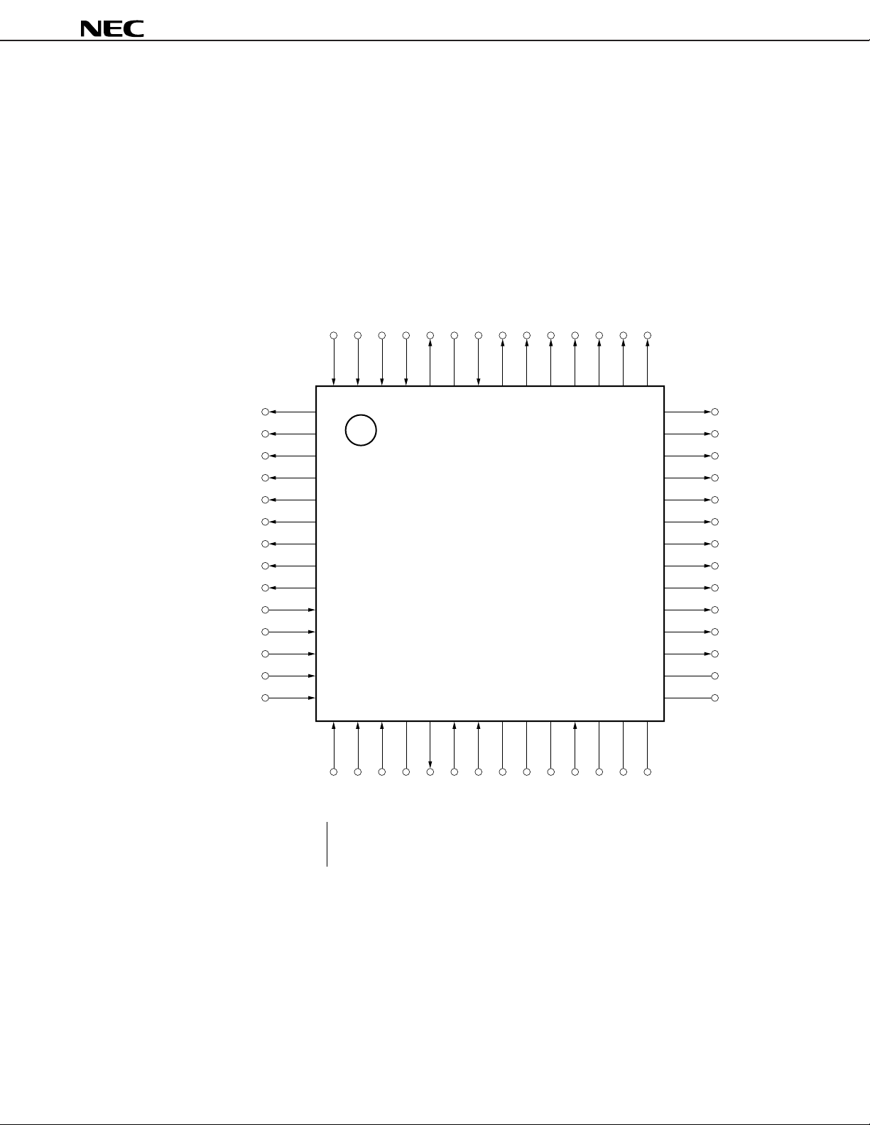
PIN CONFIGURATION (Top View)
56-pin plastic QFP (10 × 10 mm, 0.65-mm pitch)
µ
PD17071GB-012-1A7
CLKENA (P0B3)
JapanWide/100 k/200 k (P0B2)
AREA1 (P0B1)
AREA0 (P0B0)
56 55 54 53 52 51 50 49 48 47 46 45 44 43
MUTE (P1C0)
BAND1 (P0A0)
BAND2 (P0A1)
KS1 (P0A2)
KS2 (P0A3)
KS3 (P1B0)
KS4 (P1B1)
KS5 (P1B2)
KS6 (P1B3)
K0 (P1A0)
K1 (P1A1)
K2 (P1A2)
K3 (P1A3)
KEYLOCK (P0C0)
1
2
3
4
5
6
7
8
9
10
11
12
13
14
15 16 17 18 19 20 21 22 23 24 25 26 27 28
BEEPNCCE
LCD14
LCD13
LCD12
LCD11
µ
PD17071GB-012
LCD10
LCD9
LCD8
42
41
40
39
38
37
36
35
34
33
32
31
30
29
LCD7
LCD6
LCD5
LCD4
LCD3
LCD2
LCD1
LCD0
COM3
COM2
COM1
COM0
REG
CAP
LCD
LCD
1
1
STEREO (P0C1)
9 k/10 k/SD (P0D2)
Remark ( ): Pins for µPD17071GB-XXX-1A7
EO
GND
VCOL
VCOH
FMIFC/AMIFC (P0D3)
REG0
0
OUT
X
IN
X
REG1
DD
V
LCD
REG
0
LCD
CAP
7

µ
PD17071GB-012
TABLE OF CONTENTS
1. PIN FUNCTION ....................................................................................................................................9
2. CONFIGURATION OF KEY MATRIX ................................................................................................ 1 5
2.1 Layout of Initialization Diode Key Matrix .............................................................................15
2.2 Layout of Momentary Key Matrix...........................................................................................15
2.3 Connection of Key Matrix ....................................................................................................... 1 6
2.4 Description of Key Matrix ....................................................................................................... 17
2.4.1 Initialization diode matrix............................................................................................................ 17
2.4.2 Momentary key ............................................................................................................................. 20
2.5 Alarm Function ......................................................................................................................... 28
2.6 Key Lock Function...................................................................................................................2 9
3. LCD DISPLAY ....................................................................................................................................30
3.1 LCD Panel ..................................................................................................................................30
3.2 Font ............................................................................................................................................30
3.3 LCD Pattern...............................................................................................................................30
3.4 LCD Pin Assignment................................................................................................................31
3.5 Display Description .................................................................................................................33
3.6 Display Example.......................................................................................................................34
4. MUTE OUTPUT TIMING CHART ...................................................................................................... 3 6
4.1 Manual up/down (operates by pressing key and releasing within 0.5 sec) ....................36
4.2 Auto up/down (operates by holding down key for 0.5 sec or longer) .............................36
4.3 Calling Preset Memory ............................................................................................................37
4.4 Band Selection .........................................................................................................................37
4.5 C E Pi n ........................................................................................................................................37
4.5.1 High level to low level ................................................................................................................. 37
4.5.2 Low level to high level................................................................................................................. 37
4.6 Sleep Timer ...............................................................................................................................38
5. ELECTRICAL SPECIFICATIONS (PRELIMINARY).........................................................................39
6. PACKAGE ...........................................................................................................................................42
8
µ
PD17071GB-012
1. PIN FUNCTION
Pin No. Symbol Pin Name Description I/O Form
1 MUTE Mute output Outputs a mute control signal. CMOS
Outputs a high level in the following cases: push-pull
• When radio is turned ON/OFF output
• When the frequency band is changed
• During manual tuning
• During auto tuning
• When the preset memory is called
• In power-off state
2 BAND1 Band select These pins output band select signals. CMOS
3 BAND2 signal output The output of each band is as follows: push-pull
Pin BAND1 BAND2
Selected band
AM 0 0
FM 1 0
TV (1 to 3 ch)
TV (4 to 12 ch) 1 1
output
(0: Low level, 1: High level)
4 KS1 Key source Key source output pins of a key matrix CMOS
| | output push-pull
9 KS6 output
10 K0 Key return signal These pins input the key return signals of a key matrix. They are Input
| | input connected to an internal pull-down resistor.
13 K3
14 KEYLOCK Key lock signal This pin inputs a key lock signal. Input
input The signal input to this pin is used to lock or unlock a momentary key.
Input a signal to this pin as follows:
• High level: To lock the momentary key.
All momentary keys are invalid while the keys are locked.
• Low level: To unlock the keys.
Note, however, that a high level or low level of less than 32 ms is
invalid.
15 STEREO Stereo signal This pin inputs a stereo signal. Input
input Reception of stereo broadcasting is identified by the signal input to
this pin.
Input a low level to this pin while stereo broadcasting is being
received.
9
µ
PD17071GB-012
Pin No. Symbol Pin Name Description I/O Form
16 9 k/10 k AM setting input/ This pin inputs an SD (Station Detector) signal. Input
/SD SD signal input When “Europe 1” or “Europe 2” is selected as the destination region,
this pin can be also used to input setting of a channel space in an
AM band.
(1) Setting of channel space in AM band for “Europe 1” and
“Europe 2” (9 k/10k)
This setting is valid only when “Europe 1” or “Europe 2” is selected
as the destination region.
The setting is read only on power application (power-ON reset), or
when the signal input to the CE pin (pin 50) goes high (CE reset);
otherwise, it is ignored.
Input a signal to this pin as follows:
• High level: Channel space 9 kHz
• Low level: Channel space 10 kHz
Note that the setting of this pin is invalid when initialization diode
switch SD_IF = 1, and the channel space is 9 kHz.
(2) Input of SD signal (SD)
When a station has been detected this is identified by the signal
input to this pin and the frequency counter when initialization diode
switch SD_IF = 1.
Input a high level to this pin when a station is detected.
However, a signal input for less than 32 ms is invalid.
17 FMIFC FM/AM This pin inputs an intermediate frequency (IF) in an FM or AM band. Input
/AMIFC intermediate The signal input to this pin is used to identify a station.
frequency input When initialization diode switch SD_IF = 1, however, the signal input to
this pin and the signal input to the SD pin (pin 16) are used to identify
a station.
The range of the input frequency in which detection of a station is
identified is as follows:
Band Input frequency range <1> Input frequency range <2>
FM 10.7 MHz ± 20 kHz
AM 450 kHz ± 1 kHz 459/460 kHz ± 1 kHz
TV 10.7 MHz ± 20 kHz
The conditions of input frequency ranges <1> and <2> vary as follows
depending on the setting of initialization diodes IFSEL1 and IFSEL2.
IFSEL1 IFSEL2 Selected frequency range
(0: Open, 1: Short)
18 GND Ground Ground pin
0 0 Input frequency range <1>
1 0 Input frequency range <2>
0 1 Input frequency range <1>
10
µ
PD17071GB-012
Pin No. Symbol Pin Name Description I/O Form
19 EO Error out This pin outputs PLL (Phase Locked Loop) errors. CMOS
It outputs the result of comparison between the frequency input to the 3-state
VCOH (pin 21) or VCOL (pin 20) and a set frequency. output
• Input frequency > Set frequency: High level
• Input frequency < Set frequency: Low level
• Input frequency = Set frequency: Floating
Connect this pin to a varactor diode via an external LPF (lowpass
filter).
20 VCOL AM local This pin inputs local oscillation output (VCO output) in an AM band. Input
oscillation input The signal that can be input to this pin is as follows:
Selected intermediate Frequency range Minimum amplitude
frequency (MHz) (Vp-p)
10.71 MHz 5 to 50 0.2
Other than 10.71 MHz 0.3 to 8 0.2
Because an internal AC amplifier is provided, cut the DC component
of the input signal with a capacitor.
21 VCOH FM local This pin inputs local oscillation output (VCO output) in an FM and TV Input
oscillation input band. The signal that can be input to this pin is as follows:
Frequency range (MHz) Minimum amplitude (Vp-p)
4 to 230 0.2
Because an internal AC amplifier is provided, cut the DC component
of the input signal with a capacitor.
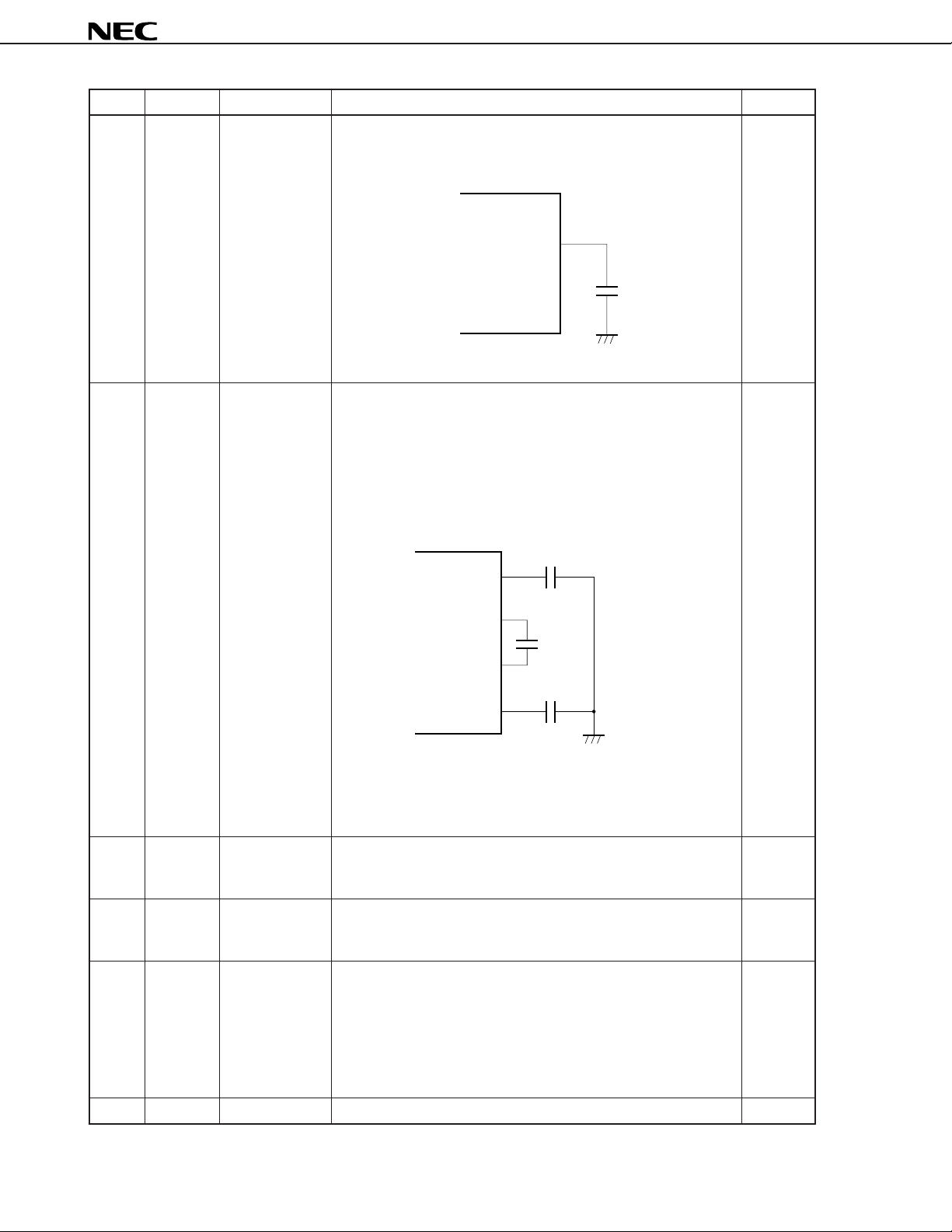
22 REG0 Power supply pin This is a voltage regulator pin for PLL. —
Connect this pin to GND via a 0.1-µF capacitor.
It outputs a low level when the radio is off.
REG0
µ
0.1 F
23 VDD Power supply pin This is a power supply pin. —
It supplies a voltage of VDD = 1.8 to 3.6 V (TA = –20 to +70 °C) to
operate all the functions.
Do not apply a voltage higher than that applied to the VDD pin to any
pin other than the VDD pin.
24 XOUT Crystal resonator These pins are used to connect a crystal resonator for system clock CMOS
oscillation. push-pull
25 XIN
Connect a 75-kHz crystal resonator across these pins.
The accuracy of the watch is affected only by the oscillation
frequency of the crystal resonator.
—
11
µ
PD17071GB-012
Pin No. Symbol Pin Name Description I/O Form
26 REG1 Power supply pin This pin is a voltage regulator pin for oscillation circuit. —
Connect this pin to GND via a 0.1-µF capacitor.
REG1
µ
0.1 F
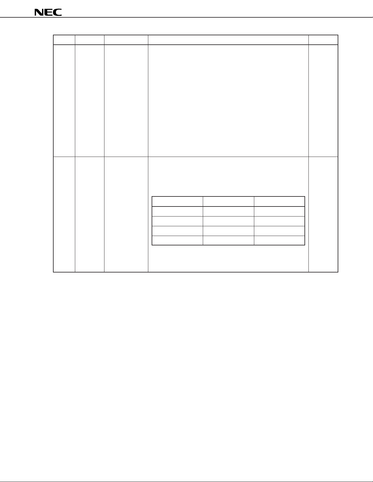
27 REGLCD0 LCD driving • REGLCD1 and REGLCD0—
28 CAP LCD0 power supply These pins supply the LCD driving voltage.
29 CAP LCD1 pins • CAPLCD1 and CAPLCD0
30 REGLCD1 Connect a capacitor for a doubler circuit across these pins to create
an LCD driving voltage.
Connect the capacitor as shown below to create the doubler circuit.
C1 = C2 = 0.1 F
C3 = 0.01 F
C1
REG
LCD
1
LCD
1
CAP
C3
CAP
LCD
0
LCD
0
REG
C2
Caution The value of the LCD drive voltage changes if the values
of C1, C2, and C3 are changed because of the configuration
of the doubler circuit.
31 COM0 LCD common These pins output common signals to an LCD panel. CMOS
| | signal output They output 60 dots on the LCD panel by creating a matrix with push-pull
34 COM3 LCD0 through LCD14 pins (pins 35 through 49). output
35 LCD0 LCD segment These pins outputs segment signals to an LCD panel. CMOS
| | signal output They display 60 dots on the LCD panel by creating a matrix with push-pull
49 LCD14 COM0 through COM3 pins (pins 31 through 34). output
50 CE Chip enable This input pins selects radio operation as follows: Input
• High level
Turns ON the radio.
• Low level
Turns OFF the radio.
Note, however, that a high or low level of less than 200 µs is not
accepted.
51 NC No connection No connection. Externally pull down this pin. —
µ
µ
12
µ
PD17071GB-012
Pin No. Symbol Pin Name Description I/O Form
52 BEEP BEEP/ALARM This pin outputs a key-ON confirmation sound (beep output) and CMOS
output alarm sound. push-pull
output
(1) Beep output
A pulse of 1.5 kHz is output for about 40 ms in the following cases:
• When a valid key is input
• While time is adjusted up or down in high-speed mode
• During seek up/down
(2) Alarm sound output
When the time reaches the alarm time set, a 3 kHz pulse is
intermittently output approximately every 64 ms, five times after 1
second.
The alarm sound is output for 10 minutes from the start of output,
or until it is canceled.
53 AREA0 Destination These pins input setting for the destination region. Input
54 AREA1 region setting The setting of these pins is read only on application of VDD (power-
input ON reset) or when the signal input to the CE pin goes high (CE
reset); otherwise, it is ignored.
Input a signal to these pins as follows:
AREA0 AREA1 Destination region
0 0 Japan
0 1 U.S.A.
1 0 Europe 1
1 1 Europe 2
(0: Low level, 1: High level)
When initialization diode switch CHINA_BAND = 1, however, the
setting is invalid, and the destination region is China.
13
µ
PD17071GB-012
Pin No. Symbol Pin Name Description I/O Form
55 Japan Wide/ FM setting input This pin inputs an FM receive frequency band and setting of a channel Input
100 k/200 k space. The setting differs depending on the destination region.
The setting is read only on application of VDD (power-ON reset) or when
the CE pin (pin 50) goes high (CE reset); otherwise, it is ignored.
(1) When the destination region is Japan (Japan Wide)
Sets an FM receive frequency band.
Input as follows:
• High-level input: 76.0 to 108.0 MHz
• Low-level input: 76.0 to 90.0 MHz
(2) When the destination region is the U.S.A. (100 k/200 k)
Sets the channel space of the FM band.
Input as follows:
• High-level input: 100-kHz step
• Low-level input: 200-kHz step
(3) When the destination region is China (100 k/200 k)
Sets the channel space of the FM band.
Input as follows:
• High-level input: 50-kHz step
• Low-level input: 100-kHz step
56 CLKENA Watch function This pin inputs the setting for whether the watch function is used or not. Input
selection input The setting is read only on application of VDD (power-ON reset) or
when the CE pin (pin 50) goes high (CE reset); otherwise, it is ignored.
Input as follows:
• High-level input: Watch function used.
• Low-level input: Watch function not used.
14
µ
PD17071GB-012
2. CONFIGURATION OF KEY MATRIX
2.1 Layout of Initialization Diode Key Matrix
Input Pin
(Pin No.)
Output Pin
(Pin No.)
KS1 (4) — CHINA_BAND TV_ENA STOPSEL
KS2 (5) SD_IF MEMSEL IFSEL1 IFSEL2
K0 (10) K1 (11) K2 (12) K3 (13)
Remark —: Not set
2.2 Layout of Momentary Key Matrix
Input Pin
(Pin No.)
Output Pin
(Pin No.)
KS3 (6) SLEEP CHECK STOP BAND
KS4 (7) AUTO STORE M4 M5 +5
KS5 (8) MEMORY/AUTO STORE M1/MEMORY UP M2 M3
KS6 (9) MODE UP DOWN ALARM
K0 (10) K1 (11) K2 (12) K3 (13)
15

2.3 Connection of Key Matrix
Momentary key
Initialization diode
Momentary key Initialization diode
Kn Kn
KsnKsn
µ
PD17071GB-012
55
56
µ
PD17071GB-012
16
15
K3K2K1K0KS6KS5KS4KS3KS2KS1
1413121110987654321
16

µ
PD17071GB-012
2.4 Description of Key Matrix
2.4.1 Initialization diode matrix
The initialization diode matrix determines the function of the µPD17071GB-012. Be sure to set this diode matrix.
The setting of the diode matrix is read only on application of VDD (power-ON reset), or when the CE pin (pin 50)
goes high (CE reset); otherwise, it is ignored.
(1) Switch setting destination region
CHINA_BAND
(2) Switch setting receivable band (valid only when the destination region is Japan)
TV_ENA
(3) Switches setting intermediate frequency of AM band
IFSEL1, IFSEL2
(4) Switch setting station detection identification method
SD_IF
(5) Switch setting momentary key for preset memory manipulation
MEMSEL
(6) Switch setting momentary key for alarm sound canceling operation
STOPSEL
To set these switches, short-circuit (1) or open (0) the corresponding switches on the matrix with a diode.
The function of the initialization diode matrix is explained next (in alphabetical order).
17

Initialization Diode Function Description
CHINA_BAND This switch selects the destination region of the application set.
Set this switch as follows:
CHINA_BAND Destination region
0 Set by AREA0 and AREA1 pins
1 China
(0: Open, 1: Short)
If China is selected as the region by this switch, the setting of AREA0 (pin 53) and AREA1 (pin 54) is invalid.
IFSEL1 This switch sets an intermediate frequency in the AM band.
IFSEL2 Set it as follows:
IFSEL1 IFSEL2 Intermediate Frequency of AM Band
0 0 450 kHz
1 0 459 kHz/460 kHz
0 1 10.71 MHz
1 1 Invalid setting.
The intermediate frequency is 450 kHz.
µ
PD17071GB-012
(0: Open, 1: Short)
When inputting an intermediate frequency to the FMIFC/AMIFC pin (pin 17) when the intermediate
frequency is set to “10.71 kHz”, convert the frequency to 450 kHz before inputting.
MEMSEL This switch sets the momentary key for preset memory manipulation.
Set it as follows:
MEMSEL Preset memory selection operation Auto store memory operation
key
M5
AUTO STORE
MEMORY
seconds or longer)
0 to key key
1 key key (hold down for 2
(0: Open, 1: Short)
SD_IF This switch selects the method for detecting a station.
Set it as follows:
SD_IF Station detection method
0 Station detection using frequency counter
1 Station detection using frequency counter and SD signal
(0: Open, 1: Short)
STOPSEL This switch sets a momentary key used to cancel alarm sound output.
It is also used to lock or unlock a key.
Set it as follows:
M1
+5
MEMORY UP
18
STOPSEL Alarm sound output canceling operation Key locking/unlocking
0 key key and key
1 key key and key
(0: Open, 1: Short)
STOP STOP
(pressed simultaneously)
ALARM
ALARM
(pressed simultaneously)
MODE
MODE

Initialization Diode Function Description
TV_ENA This switch is used to select whether a TV band is received.
Setting of this switch is valid only when Japan is selected as the destination region.
Set it as follows:
TV_ENA Receivable band when Japan is selected as region
0 FM/AM
1 FM/AM/TV
(0: Open, 1: Short)
µ
PD17071GB-012
19

2.4.2 Momentary key
Two momentary keys can be pressed simultaneously only in the following combination.
•
• and keys to lock or unlock keys
ALARM
• and keys during seek up/down
Any other combinations of keys is invalid when pressed simultaneously.
The chattering wait time is 48 to 64 ms.
The functions of the momentary keys are explained below (in alphabetical order).
and keys to lock or unlock keys
STOP
UP DOWN
MODE
MODE
µ
PD17071GB-012
20

Momentary Key Function Description
ALARM
AUTO STORE
This keys sets or cancels the alarm and cancels alarm sound output.
This key is valid when the watch function is used (when a high level is input to the CLKENA pin (pin 56)).
• When initialization diode switch STOPSEL = 0
For setting or canceling alarm
• When initialization diode switch STOPSEL = 1
For setting or canceling alarm and canceling alarm sound output
(1) Setting/canceling alarm
By pressing the key, the alarm is set at specified time.
When the key is pressed again with the alarm set, the alarm is canceled.
While the time is being adjusted and while the alarm time is being set, however, the alarm cannot be
set or canceled.
For an explanation of how to set the alarm time, refer to the description on the key.
(2) Canceling alarm sound output (when STOPSEL = 1)
By pressing the key when the alarm sound is being output, the output of the alarm can
be stopped.
(3) Locking momentary key (when STOPSEL = 1)
The momentary key is locked when the key is pressed while the key is
held down.
For key locking, refer to the description on the key.
This is a key for auto store memory.
It is valid when the radio is ON and the initialization diode switch MEMSEL = 0.
• Auto store memory
The auto store memory operation is started when the key is pressed.
This operation automatically searches a station and writes it to the preset memory.
During the auto store memory operation, the frequency being sought is displayed.
Searching is started from the lowest frequency in a band, and is completed when the highest frequency
is found.
When stations are found they are stored started from preset M1. When stations have been stored up
to M10, the auto store memory operation is completed. If the highest frequency is found before a station
is written to M10, the auto store memory operation is stopped at that point. The operation of each key
during auto store memory operation is as follows:
ALARM
ALARM
ALARM
MODE
MODE
AUTO STORE
µ
PD17071GB-012
MODE
ALARM
Key Function Description
AUTO STORE
BAND
ALARM
CHECK
STOP
Any key other than above is invalid.
Stops auto store memory operation.
• If station is written to preset memory as result of auto store memory
operation, preset M1 is received.
• If no station is written to preset memory as result of auto store memory
operation, frequency or preset station, when auto store memory operation
is started, is received.
Stops auto store memory operation and changes band.
Performs operation of pressed key.
Auto store memory operation continues.
21

Momentary Key Function Description
BAND
This key is used to select a band.
It is valid when the radio is ON.
Each time the key has been pressed, the band is changed as follows:
• If Japan is selected as destination region and if initialization diode switch TV_ENA = 1
• Other than above
BAND
(On initial power application)
FM AM TV
(On initial power application)
FM AM
µ
PD17071GB-012
CHECK
– These keys are used to call a preset station and to write data to the preset memories.
M1
MEMORY
M5
This key is used to test lighting of the LCD before shipment.
By pressing the key, all the segments of the LCD lights for 20 seconds.
If the key is pressed again while the LCD is lit, the test is stopped.
Any key other than the key is invalid during the testing of LCD lighting.
They are valid when the radio is ON and initialization diode switch MEMSEL = 0.
(1) Calling preset memory
(2) Writing preset memory
When initialization diode switch MEMSEL = 1, the key functions as the Key.
This key is for writing data to the preset memory and for auto store memory.
It is valid when the radio is ON.
• When initialization diode switch MEMSEL = 0
• When initialization diode switch MEMSEL = 1
CHECK
By pressing any of the through keys, the corresponding preset station can be
called.
A preset memory number is indicated for 0.5 second, and the corresponding frequency is selected.
Ten preset memories, M1 through M10, each corresponding to a preset station, are available.
To call preset memories M6 through M10, or to write data to these preset memories, refer to the
description of the Key.
The contents of a specified preset memory are written when one of the keys to
is pressed in combination with the key.
For how to write data to the preset memory, refer to the description of the key.
For writing preset memory
For writing preset memory and auto store memory
The operation is as follows when initialization diode switch MEMSEL = 1.
CHECK
CHECK
+5
M1
M5
MEMORY
M1
M1 M5
MEMORY
MEMORY UP
22
MEMORY
key is held down for: Operation
Less than 2 seconds Preset memory write
2 seconds or longer Auto store memory

Momentary Key Function Description
MEMORY
(1) Preset memory writing
By pressing the key, the preset memory is enabled to be written for 10 seconds.
Write data to the preset memory in the following sequence:
• When initialization diode switch MEMSEL = 0
MEMORY
Select the frequency to be stored to the memory
by using the and keys.
UP
DOWN
µ
PD17071GB-012
Press the key
to enable the preset memory to be written.
Press any of the through keys
in accordance with the preset memory to
which data is to be written, and write data to the preset memory.
• When initialization diode switch MEMSEL = 1
Select the frequency to be stored in the memory
by using the and key.
Enable the preset memory to be written
by pressing the key.
The preset memory holding the station received last plus one is
automatically selected as the preset memory to be written.
MEMORY
M1
UP
MEMORY
M5
DOWN
Select the preset memory to be written,
by using the key.
MEMORY UP
Press the key again
to write data to the preset memory.
MEMORY
23

Momentary Key Function Description
MEMORY
The operation of each key is as follows depending on the write status of the preset memory.
Key Function description
– • When initialization diode switch MEMSEL = 0
BAND
/
MODE
+5
STOP
SLEEP
M5
Data is written to a preset memory and the preset memory write
status is released.
• When initialization diode switch MEMSEL = 1
This key is invalid.
• When initialization diode switch MEMSEL = 0
This key is invalid.
• When initialization diode switch MEMSEL = 1
Increments the preset memory to be written by one station. Preset
memory M1 is selected next if preset memory M10 is selected.
• When initialization diode switch MEMSEL = 0
Releases the preset memory write status.
• When initialization diode switch MEMSEL = 1
Writes data to a preset memory and releases the preset memory
write status.
Releases the preset memory write status, and performs the operation
of the key pressed.
DOWN
Performs the operation of the key pressed.
The preset memory write status continues.
M1
MEMORY UP
MEMORY
AUTO STORE
UP
ALARM
CHECK
µ
PD17071GB-012
(2) Auto store memory (when MEMSEL = 1)
The auto store memory operation is started by holding down the key for 2 seconds or
longer.
During auto store memory operation, this key operates as the key.
For the auto store memory operation, refer to the description on the key.
MEMORY
AUTO STORE
AUTO STORE
24

Momentary Key Function Description
MEMORY UP
MODE
This key is used to call and write a preset memory.
It is valid when the radio is ON and initialization diode switch MEMSEL = 1.
(1) Calling preset memory
Each time the is is pressed, the preset station is incremented by one and called up.
The preset memory number is displayed for 0.5 second, and the corresponding frequency is received.
• When a preset station is already selected, the preset station is incremented by one and selected.
Example: When preset M3 is already selected, this is incremented by one and M4 is selected.
• If this key is pressed while no preset station is selected, preset M1 is selected.
(2) Writing preset memory
Data is written to a specified preset memory when this key is used in combination with the
key.
For an explanation of how to write data to a preset memory, refer to the description of the
key. When initialization diode switch MEMSEL = 0, this key functions as the key.
This key is used to switch the display and the watch adjust mode.
It is valid when the watch function is used (when a high level is input to the CLKENA pin (pin 56)).,
• When radio is ON: For switching display
• When radio is OFF: For switching watch adjust mode
MEMORY UP
When preset M10 is the current selection, M1 is selected next.
µ
PD17071GB-012
MEMORY
MEMORY
M1
(1) Display switching (when radio is ON)
Each time the key is pressed, the frequency display or watch display is alternately selected.
(2) Watch adjust mode switching (when radio is OFF)
Each time the key is pressed, the mode is changed as follows:
For an explanation of how to adjust the time, refer to the description of the and keys.
The momentary keys are locked by the following key operation:
• When STOPSEL = 0: Press the key and then the key twice.
• When STOPSEL = 1: Press the key and then the key twice.
While keys are locked, no key operation other than that to manipulate key locking is valid.
By repeating the key locking operation while the keys are locked, the keys are unlocked.
If the momentary keys are locked by input to the KEYLOCK pin (pin 14), the keys cannot be unlocked by
a key operation.
MODE
MODE
Watch display Alarm time setting mode Watch adjust mode
DOWN
STOP
ALARM
UP
MODE
MODE
25

Momentary Key Function Description
+5
SLEEP
STOP
This key is used to select preset memory M6 to M10 in combination with the to keys.
It is valid when the radio is ON and initialization diode switch MEMSEL = 0.
When the key is pressed, the preset shift status is set.
In this status, operating the to key manipulates preset memory M6 to M10. The preset
shift status is released on completion of the operation. If the key is pressed again in the preset
shift status, the preset shift status is released.
This key is used to set the sleep timer.
It is valid when the radio is ON.
When the key is pressed, the remaining time of the sleep timer is displayed for 10 seconds.
The initial value of the remaining time of the sleep timer is 120 minutes.
If the key is pressed while the remaining time of the sleep timer is displayed, the time is
decremented in steps of 30 minutes.
(Example 60 minutes → 30 minutes, 45 minutes → 30 minutes)
If the remaining time reaches 0 minutes, the sleep timer is released.
If the radio is turned OFF (CE = low level) while the sleep timer is valid, the sleep timer is released.
This key is used to cancel output of the alarm sound.
It is valid when the watch function is used (when a high level is input to the CLKENA pin (pin 56)).
It is valid when initialization diode switch STOPSEL = 0.
SLEEP
SLEEP
+5
M1
M5
+5
µ
PD17071GB-012
M1
M5
UP
DOWN
(1) Stopping alarm sound output
By pressing the key while the alarm sound is output, output of the alarm sound can be
stopped.
(2) Locking momentary keys (when STOPSEL = 0)
Momentary keys can be locked by pressing the key and then the key twice.
For an explanation of how to lock the keys, refer to the description of the key.
This key is used to increment/decrement the receive frequency and adjust the time.
• When radio is ON: To increment/decrement receive frequency
• When radio is OFF: To adjust time and set alarm time
(1) Incrementing/decrementing receive frequency (when radio is ON)
Time to hold down or key Operation
STOP
STOP
DOWNUP
Less than 0.5 second Increments/decrements 1 channel
0.5 second or longer Seek up/down
MODE
MODE
26

Momentary Key Function Description
UP
DOWN
The operation of each key is as follows during seek up/down operation.
Key Function description
UP
DOWN
BAND
~
M1 M5
MEMORY UP
ALARM
CHECK
+5
STOP
• If the key is pressed while the seek up operation is in progress, the seek
operation is stopped, and the frequency at which the seek operation was
started is received.
• During the seek down operation, the seek up operation is started.
• If the key is pressed while the seek down operation is in progress, the
seek operation is stopped and the frequency at which the seek operation
was started is received.
• During the seek up operation, the seek down operation is started.
Stops the seek operation and performs the operation of the key pressed.
Performs the operation of the key pressed.
The seek operation continues.
µ
PD17071GB-012
Any key other than above is invalid.
(2) Adjusting time and setting alarm time (when radio is OFF)
By pressing the or key in the alarm time setting mode or time adjust mode, the
time can be adjusted.
The following operation is performed in the alarm time setting mode and time adjust mode.
Key Digit to be Time to hold Operation
UP
DOWN
UP
adjusted down key
Minute digit Less than Increments time by 1 minute each time the key
Hour digit Less than Increments time by 1 hour each time the key is
DOWN
0.5 second is pressed.
0.5 second Fast-forward the time at a rate of 8 minutes/
or longer second until the key is released. No carry to the
hour digit occurs. Each time the minute digit has
been adjusted, the second count value is reset.
0.5 second pressed.
0.5 second Fast-forwards the time at a rate of 4 hours/
or longer second until the key is released. The minute
digit and second count value are not affected.
27

2.5 Alarm Function
The alarm function outputs an alarm sound at specified alarm time every day.
Only one alarm time can be set.
When the watch function is not selected on initialization, the alarm function cannot be used.
For initialization of the watch function, refer to the description on the CLKENA pin (pin 56).
(1) Setting of alarm time
To set alarm time, select the alarm time setting mode when the radio is OFF.
Each time the
MODE
key is pressed when the radio is OFF, the mode is changed as follows:
Watch display Alarm time setting mode Watch adjust mode
µ
PD17071GB-012
The alarm time can be adjusted by using the
and key in the alarm time setting mode.
UP DOWN
The operation is as follows in the alarm time setting mode.
Key Digit to Be Adjusted Time to Hold Down Key Operation
UP
DOWN
Minute digit Less than 0.5 second Increments the minute by one each time the key is pressed.
0.5 second or longer Increments the minute at a rate of 8 minutes/second until
key is released.
Hour digit Less than 0.5 second Increments the hour by one each time the key is pressed.
0.5 second or longer Increments the hour at a rate of 4 hours/second until the
key is released.
The initial alarm time on power application is “00:00” (midnight).
(2) Setting/releasing alarm
By pressing the
ALARM
key, the alarm is set for the time set.
When the time has reached the alarm time set, output of the alarm sound is started.
The alarm can be released by pressing the
ALARM
key again while the alarm is set.
However, the alarm cannot be set or released in the time adjust mode or alarm time setting mode.
(3) Canceling alarm sound output
Output of the alarm sound is stopped if the key for canceling the alarm sound output is pressed while the alarm
sound is being output.
The following key is used as the key for canceling the alarm sound output, depending on the initialization.
• When initialization diode switch STOPSEL = 0
key
STOP
• When initialization diode switch STOPSEL = 1
ALARM
key
The output of the alarm sound continues for 10 minutes from the start, or until it is canceled.
28

µ
PD17071GB-012
2.6 Key Lock Function
The key lock function is to lock the momentary keys and invalidate key operations.
The keys are locked by input to the KEYLOCK pin (pin 14).
When the input to the KEYLOCK pin is low, the keys can also be locked by a key operation.
(1) Locking keys by input to KEYLOCK pin (pin 14)
The momentary keys can be locked by input to the KEYLOCK pin.
The operation of the momentary keys can be manipulated as follows by the pin input.
• High-level input
Locks keys and invalidates all key operations.
Also invalidates the key operation to unlock the keys.
• Low-level input
All the keys perform normally when the keys are pressed.
At this time, the keys can be locked or unlocked by a key operation.
(2) Locking keys by key operation
The keys can be locked or unlocked by a key operation when the input to the KEYLOCK pin (pin 14) is low. If
the input to the KEYLOCK pin is high, however, the locked keys cannot be unlocked by a key operation.
The momentary keys are locked by performing the following key lock operation.
• When the keys are locked, they are unlocked when the key lock operation is performed again.
• When the keys are locked, all key operations other than that to unlock the key is invalid.
The following key lock operation is performed, depending on initialization.
• When initialization diode switch STOPSEL = 0
Press the
• When initialization diode switch STOPSEL =1
Press the key and then the key twice.
ALARM
STOP
key and then the key twice.
MODE
MODE
29

3. LCD DISPLAY
3.1 LCD Panel
The configuration of the LCD panel is shown below.
µ
PD17071GB-012
AM
AM
ALM LOCK
SLEEP
FM
PM
3.2 Font
3.3 LCD Pattern
(1) Connection of segment lines
MST+5
TV
MHz
kHz
AM
AM
ALM LOCK
SLEEP
FM
PM
LCD1
LCD0
(2) Connection of common lines
AM
AM
ALM LOCK
SLEEP
FM
PM
COM0
COM2
COM1
COM3
LCD2
LCD3
LCD4
LCD5
LCD6
LCD7
LCD8
ST
LCD9
M
LCD10
M
ST
+5
TV
MHz
kHz
LCD11
+5
TV
MHz
kHz
30

µ
PD17071GB-012
3.4 LCD Pin Assignment
Table 3-1 shows assignment of the LCD pins.
<1> through <4> in the figure and table below indicate the column positions of the 7-segment digits. “a” through
“f” indicate the segments of each digit.
MST+5
AM
AM
TV
ALM LOCK
SLEEP
FM
PM
< 1 > < 2 > < 3 > < 4 >
a
fb
MHz
kHz
g
ec
d
31

µ
PD17071GB-012
Table 3-1. Assignment of LCD Pins
Common COM0 (31) COM1 (32) COM2 (33) COM3 (34)
Segment
LCD0 (35) AM ALM SLEEP FM
LCD1 (36) AM LOCK — PM
LCD2 (37) — <1>g <1>e <1>d
LCD3 (38) <1>a <1>b <1>c —
LCD4 (39) <2>f <2>g <2>e <2>d
LCD5 (40) <2>a <2>b <2>c :
LCD6 (41) <3>f <3>g <3>e <3>d
LCD7 (42) <3>a <3>b <3>c .
LCD8 (43) <4>f <4>g <4>e <4>d
LCD9 (44) <4>a <4>b <4>c
LCD10 (45) +5 TV MHz kHz
LCD11 (46) M ST — —
LCD12 (47) ————
LCD13 (48) ————
LCD14 (49) ————
Remarks 1. Numbers in brackets ( ) are pin numbers.
2. —: Not used
32

µ
PD17071GB-012
3.5 Display Description
Symbol Description
AM Lights when the AM band is selected in the radio mode.
Lights only when a frequency is displayed.
AM Lights when the time is in the morning in the 12-hour mode.
ALM Lights while the alarm is set.
Always lights while alarm time is set, and goes off while time is being adjusted.
FM Lights when the FM band is selected in the radio mode.
Lights only when a frequency is displayed.
kHz Lights when a frequency is displayed or AM band is selected in the radio mode.
LOCK Lights when key locking is valid.
M Lights when the preset memory is manipulated in the radio mode.
Also lights at 1 Hz when the preset memory is enabled to be written.
MHz Lights when a frequency is displayed and the FM band is selected in the radio mode.
+5 Lights when +5 (preset memory shift) is valid in the radio mode.
PM Lights when the time is in the afternoon in the 12-hour mode.
SLEEP Lights when the sleep timer is set.
ST Lights when the stereo input is low in the radio mode.
TV Lights when the TV band is selected in the radio mode.
Lights only when a frequency is displayed.
Lights when time is displayed. However, blinks at 1 Hz in synchronization with time display
when the time or alarm time is adjusted.
Lights when a frequency in the FM band is selected.
Lights to indicate the least significant digit of a frequency in the FM band (part).
Lights if the least significant digit is 5 and goes off if it is 0.
Displays a frequency, time, and timer.
The high-order digits is zero-suppressed.
33

3.6 Display Example
(1) Initial display (without time set, 12-hour display)
AM
(2) Initial display (without time set, 24-hour display)
µ
PD17071GB-012
(3) Watch display (during FM band selection)
AM
This is an example of display with “M” and “+5” lit while a stereo station is selected
at 12:34 a.m.
The “FM” and “AM” indications are not displayed to avoid confusion with time when
time is displayed in the radio mode.
(4) Frequency display (during FM band selection)
FM
MST+5
MHz
34

(5) Frequency display (during AM band selection)
AM
(6) Frequency display (during TV band selection)
kHz
TV
µ
PD17071GB-012
(7) Sleep timer display
35

µ
PD17071GB-012
4. MUTE OUTPUT TIMING CHART
This section describes the timing of the mute output.
<1> through <7> in the timing charts indicate the time required for the respective processing, as follows:
<1> Key ON chattering wait time
<2> Mute leading time
<3> Division ratio setting and display contents updating time
<4> Mute trailing time
<5> Scan time
<6> PLL lock wait time
<7> Key OFF chattering wait time
4.1 Manual up/down (operates by pressing key and releasing within 0.5 sec)
Less than
0.5 sec
MUTE
< 1 >
48–64 ms
Key OFFKey ON
< 7 >
48–64 ms
< 2 >
40–48 ms
< 3 >
8–16 ms
< 4 >
250–375 ms
Time of <4> is 625 to 750 ms at the band edge.
4.2 Auto up/down (operates by holding down key for 0.5 sec or longer)
< 2 >
40–48 ms
< 3 >
8–16 ms
< 5 >
< 6 >
Without check station
< 3 >
8–16 ms
SD, IF
< 6 >
< 3 >
8–16 ms
< 6 >
MUTE
< 1 >
48–64 ms
Key ON
0.5 sec
< 5 >
SD, IF
With check station
< 4 >
250–375 ms
Scan time of <5> is as follows depending the received band.
FM: 40 to 48 ms
AM: 24 to 32 ms
TV: 496 to 504 ms
Time of <5> is 500 ms, and time of <4> is 625 to 750 ms at the band edge.
36

4.3 Calling Preset Memory
µ
PD17071GB-012
MUTE
< 1 >
48–64 ms
Key ON
< 2 >
40–48 ms
< 3 >
8–16 ms
Time of <2> to <4> is the tuner mute time.
4.4 Band Selection
MUTE
< 1 >
48–64 ms
Key ON
< 2 >
40–48 ms
< 3 >
8–16 ms
< 4 >
500–625 ms
< 4 >
500–625 ms
4.5 CE Pin
4.5.1 High level to low level
MUTE
4.5.2 Low level to high level
MUTE
8–16 ms
CE pin = high level low level
Less than 125 ms
Until the CE pin goes high next time.
< 2 >
40–48 ms
< 3 >
8–16 ms
< 4 >
496–504 ms
Tuner mute time
CE pin = low level high level
The tuner mute time is the same as 4.3 Calling Preset Memory.
37

4.6 Sleep Timer
µ
PD17071GB-012
MUTE
Until the CE pin goes high next time.
8–16 ms
Timer off time
38

µ
PD17071GB-012
5. ELECTRICAL SPECIFICATIONS (PRELIMINARY)
Absolute Maximum Ratings (TA = 25 °C)
Parameter Symbol Condition Rating Unit
Supply voltage VDD –0.3 to +4.0 V
Input voltage VI CE pin –0.3 to VDD +0.6 V
Other than CE pin –0.3 to VDD +0.3 V
Output voltage VO –0.3 to VDD +0.3 V
High-level output current IOH 1 pin –3.0 mA
Total of all pins –20.0 mA
Low-level output current IOL 1 pin 3.0 mA
Total of all pins 20.0 mA
Operating temperature TA –20 to +70 °C
Storage temperature Tstg –55 to +125 °C
Caution If any of the parameters exceeds the absolute maximum ratings, even momentarily, the quality of
the product may be impaired. The absolute maximum ratings are values that may physically damage
the product(s). Be sure to use the product(s) within the ratings.
Recommended Operating Range
Parameter Symbol Condition MIN. TYP. MAX. Unit
Supply voltage VDD1 When CPU, PLL, and AD operates 1.8 3.0 3.6 V
TA = –20 to +70 °C
VDD2 When CPU operates, TA = –10 to +70 °C 1.7 3.0 3.6 V
and PLL and AD stop TA = 0 to +70 °C 1.6 3.0 3.6 V
Supply voltage rise time tRISE VDD = 0 → 1.8 V (TA = 25 °C) 500 ms
39

µ
PD17071GB-012
DC Characteristics (TA = –20 to +70 °C, VDD = 1.8 to 3.6 V) (1/2)
Parameter Symbol Condition MIN. TYP. MAX. Unit
Supply current IDD1 When CPU and PLL are operating with sine wave 6.5 10 mA
input to VCOH pin
(fIN = 250 MHz, VIN = 0.2 Vp-p)
VDD = 3 V, TA = 25 °C
IDD2 When CPU is operating and PLL is stopped 35 45
(IF counter stops) with sine wave input to XIN pin
(fIN = 75 kHz, VIN = VDD)
VDD = 3 V, TA = 25 °C
IDD3 When CPU and PLL are stopped (when HALT 10 18
instruction is used) with sine wave input to XIN pin
(fIN = 75 kHz, VIN = VDD)
VDD = 3 V, TA = 25 °C
Data retention voltage VDDR On detection of power failure 1.7 V
Data retention current IDDR When crystal oscillator stops 3
VDD = 3.0 V, TA = 25 °C
High-level input voltage VIH1 CE, INT, P0B0-P0B3, P0C0, P0C1, P0D2, P0D3 0.8 VDD V
VIH2 P1A0-P1A3 0.5 VDD V
Low-level input voltage VIL1 CE, INT, P0B0-P0B3, P0C0, P0C1, P0D2, P0D3 0.2 VDD V
VIL2 P1A0-P1A3
High-level output current IOH1 P0A0-P0A3, P0B0-P0B3, P0C0, P0C1, –0.5 mA
P0D2, P0D3, P1B0-P1B3, P1C0, BEEP
VOH = VDD –0.5 V
IOH2 EO VOH = VDD –0.5 V –0.2 mA
IOH3 LCD0-LCD14 VOH = VDD –0.5 V –20
Low-level output current IOL1 P0A0-P0A3, P0B0-P0B3, P0C0, 0.5 mA
P0C1, P0D2, P0D3, P1C0, BEEP
VOL = 0.5 V
IOL2 EO VOL = 0.5 V 0.2 mA
IOL3 P1B0-P1B3 VOL = 0.5 V 5
IOL4 LCD0-LCD14 VOL = 0.5 V 20
High-level input current IIH1 When P1A0 through P1A3 are pulled down 3 30
VIH = VDD = 1.8 V
IIH2 When XIN pin is pulled down 40
VIH = VDD = 1.8 V
LCD drive voltage VLCD1 When LCD0 through LCD14 outputs are open 2.8 3.1 3.3 V
C1 = 0.1 µF, C2 = 0.01 µF
TA = 25 °C
Output off leakage current IL EO ±1
0.05 VDD
µ
A
µ
A
µ
A
V
µ
A
µ
A
µ
A
µ
A
µ
A
µ
A
40

µ
PD17071GB-012
AC Characteristics (TA = –20 to +70 °C, VDD = 1.8 to 3.6 V) (2/2)
Parameter Symbol Condition MIN. TYP. MAX. Unit
Operating frequency fIN1 VCOL pin, MF mode, with sine wave input 0.3 8 MHz
VIN = 0.2 Vp-p
fIN2 VCOL pin, HF mode, with sine wave input 5 130 MHz
VIN = 0.3 Vp-p
fIN3 VCOH pin, VHF mode, with sine wave input 40 230 MHz
VIN = 0.2 Vp-p
fIN4 FMIFC/AMIFC pin, AMIF count mode, 400 500 kHz
with sine wave input VIN = 0.1 Vp-p
fIN5 FMIFC/AMIFC pin, AMIF count mode, 0.4 2 MHz
with sine wave input VIN = 0.15 Vp-p
fIN6 FMIFC/AMIFC pin, FMIF count mode, 10 11 MHz
with sine wave input VIN = 0.1 Vp-p
A/D Converter Characteristics (TA = –20 to +70 °C, VDD = 1.8 to 3.6 V)
Parameter Symbol Condition MIN. TYP. MAX. Unit
A/D conversion resolution 4 bit
A/D conversion total error TA = 25 °C ±1.5 LSB
41

6. PACKAGE
56 PIN PLASTIC QFP (10 10)
µ
PD17071GB-012
A
B
43
42
29
28
CD
56
1
14
15
F
J
G
H
P
M
I
K
M
N
NOTE
Each lead centerline is located within 0.13 mm (0.005 inch) of
its true position (T.P.) at maximum material condition.
L
detail of lead end
S
+0.10
–0.05
R
0.504±0.016
0.031
0.031
0.005
0.026 (T.P.)
0.055±0.008
0.004
5°±5°
0.079 MAX.
S56GB-65-1A7-3
+0.008
–0.009
+0.004
–0.003
Q
ITEM MILLIMETERS INCHES
A 12.8±0.4 0.504±0.016
B 10.0±0.2 0.394±0.008
C 10.0±0.2 0.394±0.008
D
12.8±0.4
F
0.8
G
0.8
H 0.30±0.10 0.012±0.004
I
0.13
J
0.65 (T.P.)
K
1.4±0.2
L 0.6±0.2 0.024
M 0.15 0.006
N 0.10
P 1.7 0.067
Q
0.125±0.075 0.005±0.003
R
5°±5°
S
2.0 MAX.
42

[MEMO]
µ
PD17071GB-012
43

[MEMO]
µ
PD17071GB-012
44

[MEMO]
µ
PD17071GB-012
45

µ
PD17071GB-012
NOTES FOR CMOS DEVICES
1 PRECAUTION AGAINST ESD FOR SEMICONDUCTORS
Note: Strong electric field, when exposed to a MOS device, can cause destruction
of the gate oxide and ultimately degrade the device operation. Steps must
be taken to stop generation of static electricity as much as possible, and
quickly dissipate it once, when it has occurred. Environmental control must
be adequate. When it is dry, humidifier should be used. It is recommended
to avoid using insulators that easily build static electricity. Semiconductor
devices must be stored and transported in an anti-static container, static
shielding bag or conductive material. All test and measurement tools
including work bench and floor should be grounded. The operator should
be grounded using wrist strap. Semiconductor devices must not be touched
with bare hands. Similar precautions need to be taken for PW boards with
semiconductor devices on it.
2 HANDLING OF UNUSED INPUT PINS FOR CMOS
Note: No connection for CMOS device inputs can be cause of malfunction. If no
connection is provided to the input pins, it is possible that an internal input
level may be generated due to noise, etc., hence causing malfunction. CMOS
device behave differently than Bipolar or NMOS devices. Input levels of
CMOS devices must be fixed high or low by using a pull-up or pull-down
circuitry. Each unused pin should be connected to VDD or GND with a
resistor, if it is considered to have a possibility of being an output pin. All
handling related to the unused pins must be judged device by device and
related specifications governing the devices.
3 STATUS BEFORE INITIALIZATION OF MOS DEVICES
Note: Power-on does not necessarily define initial status of MOS device. Produc-
tion process of MOS does not define the initial operation status of the device.
Immediately after the power source is turned ON, the devices with reset
function have not yet been initialized. Hence, power-on does not guarantee
out-pin levels, I/O settings or contents of registers. Device is not initialized
until the reset signal is received. Reset operation must be executed immediately after power-on for devices having reset function.
46

µ
PD17071GB-012
Regional Information
Some information contained in this document may vary from country to country. Before using any NEC
product in your application, please contact the NEC office in your country to obtain a list of authorized
representatives and distributors. They will verify:
• Device availability
• Ordering information
• Product release schedule
• Availability of related technical literature
• Development environment specifications (for example, specifications for third-party tools and
components, host computers, power plugs, AC supply voltages, and so forth)
• Network requirements
In addition, trademarks, registered trademarks, export restrictions, and other legal issues may also vary
from country to country.
NEC Electronics Inc. (U.S.)
Santa Clara, California
Tel: 800-366-9782
Fax: 800-729-9288
NEC Electronics (Germany) GmbH
Duesseldorf, Germany
Tel: 0211-65 03 02
Fax: 0211-65 03 490
NEC Electronics (Germany) GmbH
Benelux Office
Eindhoven, The Netherlands
Tel:040-2445845
Fax: 040-2444580
NEC Electronics (France) S.A.
Velizy-Villacoublay, France
Tel:01-30-67 58 00
Fax: 01-30-67 58 99
NEC Electronics Hong Kong Ltd.
Hong Kong
Tel:2886-9318
Fax: 2886-9022/9044
NEC Electronics Hong Kong Ltd.
Seoul Branch
Seoul, Korea
Tel: 02-528-0303
Fax: 02-528-4411
NEC Electronics (UK) Ltd.
Milton Keynes, UK
Tel: 01908-691-133
Fax: 01908-670-290
NEC Electronics Italiana s.r.1.
Milano, Italy
Tel: 02-66 75 41
Fax: 02-66 75 42 99
NEC Electronics (France) S.A.
Spain Office
Madrid, Spain
Tel: 01-504-2787
Fax: 01-504-2860
NEC Electronics (Germany) GmbH
Scandinavia Office
Taeby, Sweden
Tel: 08-63 80 820
Fax: 08-63 80 388
NEC Electronics Singapore Pte. Ltd.
United Square, Singapore 1130
Tel:253-8311
Fax: 250-3583
NEC Electronics Taiwan Ltd.
Taipei, Taiwan
Tel: 02-719-2377
Fax: 02-719-5951
NEC do Brasil S.A.
Sao Paulo-SP, Brasil
Tel: 011-889-1680
Fax: 011-889-1689
J96. 8
47

µ
PD17071GB-012
[MEMO]
Purchase of NEC I2C components conveys a license under the Philips I2C Patent Rights to use these components
in an I2C system, provided that the system conforms to the I2C Standard Specification as defined by Philips.
No part of this document may be copied or reproduced in any form or by any means without the prior written
consent of NEC Corporation. NEC Corporation assumes no responsibility for any errors which may appear in
this document.
NEC Corporation does not assume any liability for infringement of patents, copyrights or other intellectual property
rights of third parties by or arising from use of a device described herein or any other liability arising from use
of such device. No license, either express, implied or otherwise, is granted under any patents, copyrights or other
intellectual property rights of NEC Corporation or others.
While NEC Corporation has been making continuous effort to enhance the reliability of its semiconductor devices,
the possibility of defects cannot be eliminated entirely. To minimize risks of damage or injury to persons or
property arising from a defect in an NEC semiconductor device, customers must incorporate sufficient safety
measures in its design, such as redundancy, fire-containment, and anti-failure features.
NEC devices are classified into the following three quality grades:
"Standard", "Special", and "Specific". The Specific quality grade applies only to devices developed based on a
customer designated "quality assurance program" for a specific application. The recommended applications of
a device depend on its quality grade, as indicated below. Customers must check the quality grade of each device
before using it in a particular application.
Standard: Computers, office equipment, communications equipment, test and measurement equipment,
audio and visual equipment, home electronic appliances, machine tools, personal electronic
equipment and industrial robots
Special: Transportation equipment (automobiles, trains, ships, etc.), traffic control systems, anti-disaster
systems, anti-crime systems, safety equipment and medical equipment (not specifically designed
for life support)
Specific: Aircrafts, aerospace equipment, submersible repeaters, nuclear reactor control systems, life
support systems or medical equipment for life support, etc.
The quality grade of NEC devices is "Standard" unless otherwise specified in NEC's Data Sheets or Data Books.
If customers intend to use NEC devices for applications other than those specified for Standard quality grade,
they should contact an NEC sales representative in advance.
Anti-radioactive design is not implemented in this product.
48
M4 96.5
 Loading...