

查询UPD168110供应商
DESCRIPTION
The µPD168110 is a monolithic 2-channel H bridge driver that consists of a CMOS controller and a MOS output
stage. It can reduce the current consumption and the voltage loss at the output stage compared with a conventional
driver using bipolar transistors, thanks to employment of a MOS process. This product employs a P-channel
MOSFET on the high side of the output stage, eliminating a charge pump. As a result, the circuit current consumption
can be substantially reduced during operation.
This product is ideal for driving the motor of a digital still camera as it can switch over between two-phase excitation
driving and microstep driving, using a stepper motor.
FEATURES
O Two H bridge circuits employing power MOSFET
O Current feedback 64-step microstep driving and two-phase excitation driving selectable
O Low on-resistance: 2 Ω MAX.
O 3 V power supply
Minimum operating power supply voltage V
O Under voltage lockout circuit
Shuts down internal circuitry at V
O 24-pin TSSOP
ORDERING INFORMATION
Part Number Package
MICROSTEP DRIVER FOR DRIVING CAMERA LENS
µ
PD168110MA-6A5 24-pin plastic TSSOP (5.72 mm (225))
DATA SHEET
DD = 2.7 V
DD = 1.7 V TYP.
MOS INTEGRATED CIRCUIT
µ
PD168110
The information in this document is subject to change without notice. Before using this document, please
confirm that this is the latest version.
Not all products and/or types are available in every country. Please check with an NEC Electronics
sales representative for availability and additional information.
Document No. S15840EJ2V0DS00 (2nd edition)
Date Published June 2005 NS CP(K)
Printed in Japan
The mark shows major revised points.
2003
µ
PD168110
PIN FUNCTIONS
Package: 24-pin TSSOP
MODE
CLK
LGND
C
OSC
MOB
PGND2
OUT2B
V
OUT2A
FB2
PS
OE
1
2
3
4
5
6
7
M2
8
9
10
11
12
24
23
22
21
20
19
18
17
16
15
14
13
RESETB
CW
DD
V
FIL2
FIL1
FB1
OUT1B
M1
V
OUT1A
PGND1
MOBSEL
STOP
Pin No. Pin Name Pin Function
1 MODE Microstep/2-phase excitation switch pin
2 CLK Pulse input pin
3 LGND Control block GND pin
4 COSC Pin connecting capacitor for output oscillator
5 MOB Phase detection output pin
6 PGND2 Output block GND pin
7 OUT2B Channel 2 output B
8 VM2 Motor power pin
9 OUT2A Channel 2 output A
10 FB2 Channel 2 current detection resistor connecting pin
11 PS Power save mode pin
12 OE Output enable pin
13 STOP Stop mode pin
14 MOBSEL MOB output select pin
15 PGND1 Output block GND pin
16 OUT1A Channel 1 output A
17 VM1 Motor power pin
18 OUT1B Channel 1 output B
19 FB1 Channel 1 current detection resistor connecting pin
20 FIL1 Channel 1 filter capacitor connecting pin
21 FIL2 Channel 2 filter capacitor connecting pin
22 VDD Control block power pin
23 CW Revolution direction setting pin
24 RESETB Reset input pin
2
Data Sheet S15840EJ2V0DS
µ
PD168110
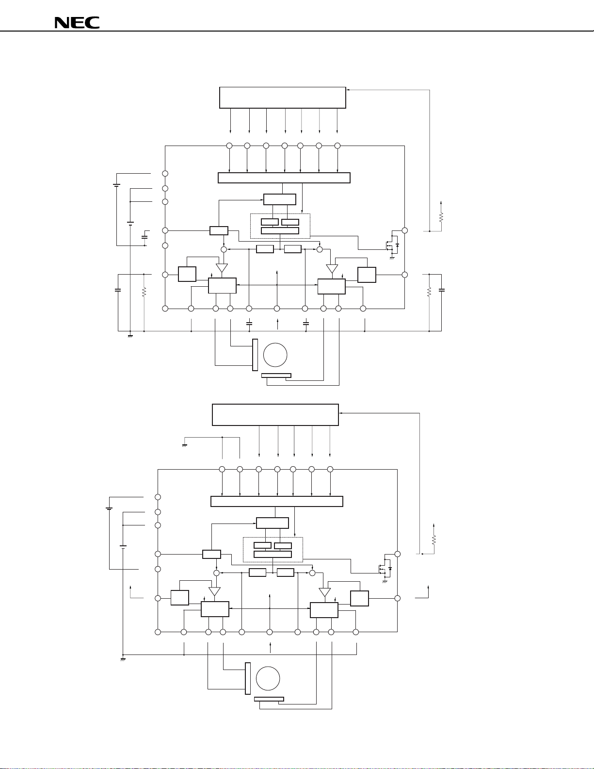
BLOCK DIAGRAM
V
DD
V
M1
V
M2
MODE MOBSEL
RESET CLK
DECODER
PULSE
GENERATER
CW PS STOP
C
OSC
LGND
FB1
Current
Sense1
PGND
EVR1
OSC
++
+
–
V
M
H BRIDGE
ch1
OUT1A OUT1B
CURRENT SET
FILTER FILTER
Internal Block
FIL1 OE FIL2
EVR2
+
–
M
V
H BRIDGE
ch2
OUT2A OUT2B
Current
Sense2
PGND
Truth Table
RESET CLK CW OE PS STOP MODE MOBSEL Operation Mode
H
H
H
H
H
H
H X X L X X X X Output Hi-Z
H X X H L H H X
H X X H H H H X
H X X H H L H X Setting prohibited
L X X X X X X X Reset mode
L H L L H L
H H L L H L
L H L L H H
H H L L H H
L H L L L X 2-phase CW mode
H H L L L X 2-phase CCW mode
Microstep CW mode
MOB: 1 pulse/cycle
Microstep CCW mode
MOB: 1 pulse/cycle
Microstep CW mode
MOB: 4 pulses/cycle
Microstep CCW mode
MOB: 4 pulses/cycle
STOP mode after MOB = L
(CLK must be input until MOB = L)
PS mode after MOB = L
(CLK must be input until MOB = L)
MOB
FB2
H: High level, L: Low level, X: High level or low level
Data Sheet S15840EJ2V0DS
3
µ
PD168110
Command Input Timing Chart
In microstep mode
RESET
CLK
CW
OE
PS
STOP
PULSE
OUT
(internal)
Chopping pulse
MOB
Reset status
1
2 3 4 5 6 7 8 9 1011 12 13 14 1516
12 345678910111213 1314 1415 1516 17 18 17 16
Output when MOBSEL = H
CW mode
17 1819 20 21 22 23 24 25 26272829 30
Power save mode
STOP mode
stopped
CCW mode Reset status
Output Hi-Z
4
Data Sheet S15840EJ2V0DS
µ
PD168110
Standard Connection Diagram
Microstep/2-phase excitation driving
CPU
DD
5.0 V
330 pF
V
V
V
C
LGND
FB1
2 kΩ
M1
M2
OSC
Current
Sense1
PGND
3.3 V
Only 2-phase excitation driving
DECODER
PULSE
EVR2
1000 pF
from CPU
M
CPU
CW PS STOP
–
H BRIDGE
ch2
OUT2A OUT2B
M
V
Current
Sense2
PGND
MODE MOBSEL
OSC
++
++–
V
M
H BRIDGE
ch1
OUT1A OUT1B
RESET CLK
GENERATER
EVR1
CURRENT SET
FILTER FILTER
Internal Block
FIL1 OE FIL2
1000 pF
MOB
FB2
2 kΩ
V
10 kΩ
DD
1000 pF1000 pF
3.3 V
5.0 V
V
MODE MOBSEL
V
DD
V
M1
V
M2
C
OSC
LGND
DD
Current
FB1
Sense1
PGND
OSC
++–
V
M
H BRIDGE
ch1
OUT1A OUT1B
RESET CLK
DECODER
PULSE
GENERATER
EVR1
CURRENT SET
FILTER FILTER
Internal Block
FIL1 OE
EVR2
From CPU
M
CW PS STOP
++
–
H BRIDGE
ch2
FIL2
OUT2A OUT2B
DD
V
10 kΩ
MOB
V
DD
M
V
Current
Sense2
PGND
FB2
Data Sheet S15840EJ2V0DS
5
µ
PD168110
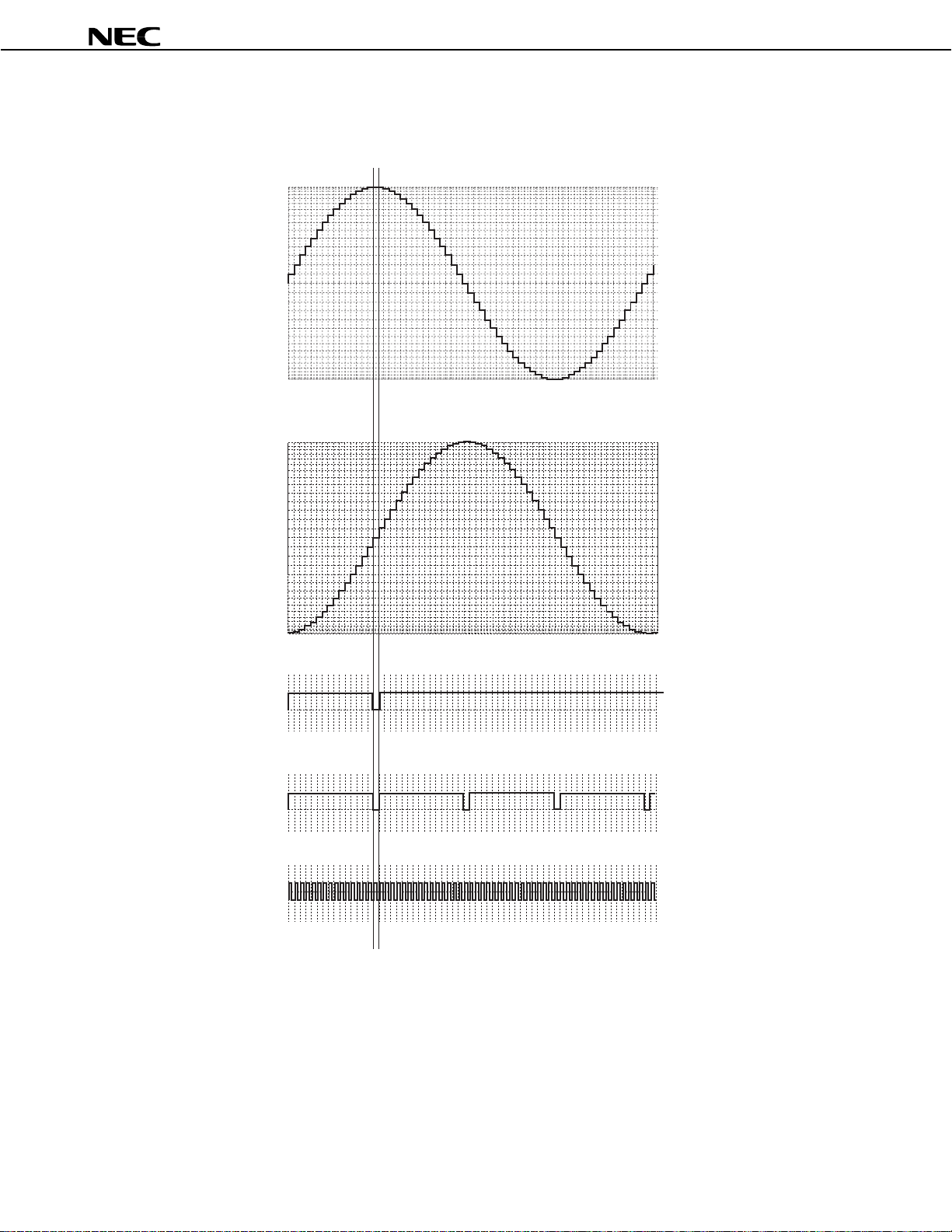
Output Timing Chart
• Microstep output mode
100
99.5
98.1
95.7
92.4
88.2
83.1
77.3
70.7
63.4
55.6
47.1
38.3
29.0
19.5
9.8
0
–9.8
–19.5
–29.0
–38.3
–47.1
–55.6
–63.4
–70.7
–77.3
–83.1
–88.2
–92.4
–95.7
–98.1
–99.5
–100
0510
position
Ch 1 current
15 20 25 30 35 40 45 50 55 60 65
100
Ch 2 current
99.5
98.1
95.7
92.4
88.2
83.1
77.3
70.7
63.4
55.6
47.1
38.3
29.0
19.5
9.8
0
—
9.8
—
19.5
—
29.0
—
38.3
—
47.1
—
55.6
—
63.4
—
70.7
—
77.3
—
83.1
—
88.2
—
92.4
—
95.7
—
98.1
—
99.5
—
100
0 5 10 15 20 25 30 35 40 45 50 55 60 65
0 5 10 15 20 25 30 35 40 45 50 55 60 65
0
5 101520253035404550556065
MOB output (when MOBSEL = “L”)
MOB output (when MOBSEL = “H”)
CLK input
0 5 10 15 20 25 30 35 40 45 50 55 60 65
The horizontal axis indicates the number of steps. This figure shows an example in the CW mode. The pulse
advances in synchronization with the rising edge of CLK. The current flows into ch 1 and ch 2 in the positive direction
when it flows from OUT1A to OUT1B, and in the negative direction when it flows from OUT1B to OUT1A (the values
shown above are ideal values and do not indicate the actual values).
6
Data Sheet S15840EJ2V0DS

µ
Output Timing Chart
• 2-phase excitation output mode
Ch 1 current
100
–100
012345678
Ch 2 current
100
PD168110
–100
012345678
MOB output
012345678
CLK input
012345678
The horizontal axis indicates the number of steps. This figure shows an example in the CW mode. The current
flows into ch 1 and ch 2 in the positive direction when it flows from OUT1A to OUT1B, and in the negative direction
when it flows from OUT1B to OUT1A.
Data Sheet S15840EJ2V0DS
7

µ
PD168110
Relationship Between Revolution Angle, Phase Current, and Vector Amount (64 microsteps)
Step
θ
0 0
θ
1 5.625 2.5 9.8 17.0 94.5 100 104.5 100.48
θ
2 11.250 12.4 19.5 26.5 93.2 98.1 103.0 100
θ
3 16.875 22.1 29.0 36.1 90.7 95.7 100.7 100.02
θ
4 22.500 31.3 38.3 45.3 87.4 92.4 97.4 100.02
θ
5 28.125 40.1 47.1 54.1 83.2 88.2 93.2 99.99
θ
6 33.750 48.6 55.6 62.6 78.1 83.1 88.1 99.98
θ
7 39.375 58.4 63.4 68.4 72.3 77.3 82.3 99.97
θ
8 45 65.7 70.7 75.7 65.7 70.7 75.7 99.98
θ
9 50.625 72.3 77.3 82.3 58.4 63.4 68.4 99.97
θ
10 56.250 78.1 83.1 88.1 48.6 55.6 62.6 99.98
θ
11 61.875 83.2 88.2 93.4 40.1 47.1 54.1 99.99
θ
12 67.500 87.4 92.4 97.4 31.3 38.3 45.3 100.02
θ
13 73.125 90.7 95.7 100.7 22.1 29.0 36.1 100.02
θ
14 78.750 93.2 98.1 103.0 12.4 19.5 26.5 100
θ
15 84.375 94.5 100 104.5 2.5 9.8 17.0 100.48
θ
16 90
Revolution
Angle
Phase A – Phase Current Phase B – Phase Current Vector Amount
Min. Typ. Max. Min. Typ. Max. Typ.
−
−
0 3.8
100
− −
−
100
0 3.8 100
−
100
The above values are ideal values and are not guaranteed values.
8
Data Sheet S15840EJ2V0DS

µ
PD168110
FUNCTION DESCRIPTION
2-phase excitation driving mode
By allowing a current of ±100% to flow into output ch1 and ch2 at the same time, a motor can be driven with the
larger torque.
The two-phase excitation driving mode and microstep driving mode are switched by the MODE pin. In the two-
phase excitation driving mode, the chopping pulse circuit does not operate.
Microstep driving of stepper motor
To position a stepper motor with high accuracy, the
through the H bridge by a vector value and to stop one cycle in 64 steps. To realize the microstep driving mode, the
driver internally realizes the following functions.
• Detecting the current flowing into each channel as a voltage value by a sense resistor
• Synthesizing the dummy sine wave of the half-wave generated by the internal D/A and PWM oscillation wave for
chopping operation
• The driver stage performs PWM driving based on the result of comparing the detected voltage value and
synthesized waves.
The internal dummy sine wave is of 64 steps per cycle, so that the stepper motor can be driven in 64 steps. The
microstep driving mode and two-phase excitation driving mode are switched by an external pin.
µ
PD168110 has a function to hold constant the current flowing
+
M
A
Concept of microstep driving operation
MOB output
The MOB output pin outputs “L” if the current of ch1 or ch2 reaches ±100% in the microstep output mode, or if the
current of ch 1 reaches +100%. In the two-phase excitation output mode, the MOB pin outputs “L” when the current of
ch1 and ch2 reaches +100%. The excitation position of the stepper motor can be checked by monitoring the MOB
output. The MOB output also indicates the stop position information in the stop mode to be explained below.
The MOB output goes into a Hi-Z state (output H level if pulled up) when OE = “L”.
Stop mode
If the stop mode is set by the STOP pin, the pulse is automatically output until MOB = “L” when CLK is input. If
MOB = “L” in the stop mode, the pulse is not output even when CLK is input, and the output holds the excitation
status.
To advance the pulse, release the stop mode and restore the normal mode.
Data Sheet S15840EJ2V0DS
9

µ
PD168110
Reset function
When RESET = “L”, initialization is executed and the output goes into a Hi-Z state. When RESET = “H”, excitation
is started with the current of ch1 at +100% and the current of ch2 at 0% (one-phase excitation position). To perform
two-phase excitation driving, excitation is started with the currents of ch1 and ch2 at +100% after the mode has been
set. Be sure to execute a reset operation after power application. MOB outputs “L” until the pulse is output when
RESET goes “L”.
Output enable (OE) pin
The pulse output can be forcibly stopped from an external source by using the OE pin. When OE = “L”, the output
is forcibly made to go into a Hi-Z state.
Standby function
The
µ
PD168110 can enter the standby mode when the pulse is not output and when PS = “H” and
STOP = “H”. In the standby mode, as many internal circuits as possible are stopped so that the self current
consumption can be reduced. In the standby mode, the current consumption is 1
stopped. While CLK is being input, the current consumption is reduced to 300
µ
A MAX. when external CLK input is
µ
A MAX. by the current flowing into the
input buffer. The standby mode is released when PS = “L” and STOP = “L”.
Under voltage lockout circuit (UVLO)
This function is used to forcibly stop the operation of the IC to prevent malfunction of the circuits if V
drops during operation. Note that if the V
DD voltage abruptly drops in the order of
µ
s, this function may not operate.
DD of the IC
V
M pin current shutdown circuit
A circuit that prevents a current from flowing into the VM pin when V
flowing into the VM pin is cut off when V
A current of up to 3
µ
A flows into the VM pin when VDD is applied so that the voltages on the VDD and VM pins can
DD = 0 V.
DD = 0 V is provided. Therefore, the current
be monitored.
10
Data Sheet S15840EJ2V0DS

µ
PD168110
OPERATION DESCRIPTION
• Setting output current
The peak value of the output current (when current of ch 1 or ch 2 is 100%) is determined by the resistor R
is connected to FB1 and FB2. This IC has an internal reference power supply V
current, and drives the stepper motor with the current value calculated by R
REF (500 mV TYP.) for comparing
FB and VREF as the peak output
current value.
Peak output current value I
MAX (A) ≅ VREF (V) ÷ RFB (Ω) x Output detection ratio
• Pulse output
The motor is driven by inputting a pulse to the CLK pin. The motor advances by one pulse at the rising edge of
the CLK signal. When MODE = “H”, the motor is driven in the 64-microstep driving mode, and the driving current
of each step is determined based on the internal motor excitation position information and revolution direction.
When MODE = “L”, the two-phase excitation mode is selected, and the current direction (100% drive) of ch 1 and
ch 2 are switched each time a pulse has been input.
• Setting motor revolution direction
The revolution direction of the motor is set by CW. In the CW mode (CW = “L”), the current of ch2 is output, 90°
degrees in phase behind the current of ch1. In the CCW mode (CW = “H”), the current of ch2 is output, 90°
degrees in phase ahead of the current of ch1.
CW Pin Operation Mode
FB that
L CW mode (forward revolution)
H CCW mode (reverse revolution)
• Setting stop mode (valid only in microstep driving mode)
When STOP = “H”, the motor advances to the position of MOB output = “L”, and the output status is held.
The excitation status is not changed even when a pulse is input to CLK while MOB = “L” when STOP = “H”. The
pulse can be advanced when STOP = “L”.
STOP Operation Mode
L Normal mode
H Stop mode
Caution If STOP = “L” before the stop mode is set (until MOB = “L”), the operation is performed in the
same manner as in the normal mode.
Data Sheet S15840EJ2V0DS
11

µ
PD168110
• Power save mode (valid only in microstep driving mode)
When PS = “H” and STOP = “H”, the motor advances to the position of MOB output = “L” and then the output
goes to a Hi-Z state.
The internal circuitry is stopped as much as possible and the standby mode is set. The power save mode is
released when PS = “L” and STOP = “L”.
STOP Operation Mode
L Normal mode
H Power save mode (only when STOP = “H”)
Caution Inputting PS = “H” and STOP = “L” is prohibited.
• Setting output enable
When OE = “H”, the motor is driven (output excitation status). Be sure to set OE to “H” to drive the motor.
STOP Operation Mode
L Output Hi-Z
H Enable mode
• Selecting two-phase excitation/microstep driving mode
The MODE pin can be used to select the two-phase excitation or microstep driving mode. When MODE = “H”,
the microstep driving mode is selected. When MODE = “L”, the two-phase excitation mode (both ch 1 and ch 2
are driven at +100% or –100%) is selected. The
µ
PD168110 is initialized immediately after a RESET operation,
so excitation is started from the position at which the output current of ch 1 is 100% and the output current of ch
2 is 0% in the microstep driving mode, and from the position at which the output currents of both ch 1 and ch 2
are +100% in the two-phase excitation driving mode.
If the mode is changed from the microstep to the two-phase, the position of the microstep mode is retained until
CLK is input. When the first CLK is input, pulse output is started, the operation skips to the two-phase position of
the next quadrant, and driving is started.
MODE Operation Mode
L 2-phase excitation
H Microstep driving
Microstep stop
position
(example 2)
(3)
Microstep stop position
(example 1)
2-phase
excitation stop
(1)
position
Skips to next quadrant
(2)
Concept of switching operation mode
from microstep to 2-phase excitation
12
Data Sheet S15840EJ2V0DS

µ
PD168110
• Selecting MOB output (in microstep driving mode only)
The output function of MOB can be selected by MOBSEL. When MOBSEL = “L”, MOB is output at the position
where the current of ch1 is +100% and the current of ch2 is 0%. When MOBSEL = “H”, MOB is output at the
position where the current of ch1 or ch2 is ±100%.
MOBSEL MOB Output
L Current of ch1 is +100% and current of ch2 is 0% (1 pulse/cycle).
H Current of ch1 or ch2 is ±100% (4 pulses/cycle).
RESET position
100
99.5
98.1
95.7
92.4
88.2
83.1
77.3
70.7
63.4
55.6
47.1
38.3
29.0
19.5
9.8
0
—
9.8
—
19.5
—
29.0
—
38.3
—
47.1
—
55.6
—
63.4
—
70.7
—
77.3
—
83.1
—
88.2
—
92.4
—
95.7
—
98.1
—
99.5
—
100
0 5 10 15 20 25 30 35 40 45 50 55 60 65
100
99.5
98.1
95.7
92.4
88.2
83.1
77.3
70.7
63.4
55.6
47.1
38.3
29.0
19.5
9.8
0
—
9.8
—
19.5
—
29.0
—
38.3
—
47.1
—
55.6
—
63.4
—
70.7
—
77.3
—
83.1
—
88.2
—
92.4
—
95.7
—
98.1
—
99.5
—
100
0 5 10 15 20 25 30 35 40 45 50 55 60 65
Ch 1 current
Ch 2 current
MOB output MOBSEL = “L”
0 5 10 15 20 25 30 35 40 45 50 55 60 65
MOB output MOBSEL = “H”
0 5 10 15 20 25 30 35 40 45 50 55 60 65
Data Sheet S15840EJ2V0DS
13

µ
PD168110
ABSOLUTE MAXIMUM RATINGS
(T
A = 25°C: GLASS EPOXY BOARD OF 100 mm × 100 mm × 1 mm WITH C OPPER FOIL OF 15%)
Parameter Symbol Conditions Rating Unit
VDD Control block −0.5 to +6.0 Power supply voltage
V
M Motor block −0.5 to +6.0
Input voltage VIN −0.5 to VDD +0.5 V
Output pin voltage VOUT 6.2 V
DC output current ID(DC) DC ±0.4 A/ch
Instantaneous output current ID(pulse) PW < 10 ms, Duty 20% ±0.7 A/ch
Power consumption PT 0.7 W
Peak junction temperature TCH(MAX) 150 °C
Storage temperature Tstg −55 to +150 °C
V
RECOMMENDED OPERATING CONDITIONS
(T
A = 25°C: GLASS EPOXY BOARD OF 100 mm × 100 mm × 1 mm WITH COPPER FOIL OF 15%)
Parameter Symbol Conditions MIN. TYP. MAX. Unit
VDD Control block 2.7 3.6 V Power supply voltage
V
M Motor block 2.7 5.5 V
Input voltage VIN 0 VDD V
DC output current ID(DC) DC −0.35 +0.35 A/ch
Instantaneous output current ID(pulse) PW < 10 ms, Duty ≤ 20% −0.6 +0.6 A/ch
MOB pin output sink current IMOB Open-drain output 5 mA
Operating temperature range TA −10 75 °C
14
Data Sheet S15840EJ2V0DS

µ
PD168110
ELECTRICAL CHARACTERISTICS (UNLESS OTHERWISE SPECIFIED, VDD = VM = 3 V, TA = 25°C)
Parameter Symbol Conditions MIN. TYP. MAX. Unit
VDD pin current after reset IDD(STB) External CLK stopped 1.0
IDD(STB2) External CLK stopped 30
I
DD(STB3) External CLK is input 300
VDD pin current during operation IDD(ACT) 3.0 mA
VM pin current
High-level input current IIH VIN = VDD 1.0
Low-level input current IIL VIN = 0 V −1.0 µA
High-level input voltage VIH 2.7 V ≤ VDD ≤ 3.6 V 0.7 x VDD V
Low-level input voltage VIL 2.7 V ≤ VDD ≤ 3.6 V 0.3 x VDD V
Input hysteresis voltage Vhys 0.3 V
H bridge on-resistance
Output turn-on time tON 0.02 0.5
Output turn-off time tOFF
Internal reference voltage VREF 450 500 550 mV
Output detection ratio
I
M(OFF)
R
ON
M
= 5.5 V per VM pin, after reset
V
and in standby mode
M = 0.35 A, sum of upper and
I
lower stages,
FB1 = FB2 = 0 V
M
= 20 Ω
R
OE pin ↑ → output SW time
IM = 0.1 A, with 5 kΩ sense
resistor connected
3.0
2.0
0.02 0.5
950 1050 1150
µ
A
µ
A VDD pin current in standby mode
µ
A
µ
A
µ
A
Ω
µ
s
µ
s
Cautions 1. The undervoltage lockout detection circuit (UVLO) operates at 1.7 V TYP. whereupon the
output goes into a Hi-Z state. Internal data such as the excitation position information is
reset. The UVLO circuit does not operate after reset.
2. A shutdown circuit that prevents a current from flowing into the V
M pin when VDD = 0 V is
provided.
Data Sheet S15840EJ2V0DS
15

µ
PD168110
PACKAGE DRAWING
24-PIN PLASTIC TSSOP (5.72 mm (225))
24
13
detail of lead end
F
G
R
P
L
S
1
A
A'
12
E
H
I
J
S
C
K
SN
DM
NOTE
Each lead centerline is located within 0.10 mm of
its true position (T.P.) at maximum material condition.
M
B
ITEM MILLIMETERS
A
6.65±0.10
6.5±0.1
A'
0.575
B
0.5 (T.P.)
C
0.22±0.05
D
0.1±0.05
E
F
1.2 MAX.
1.0±0.05
G
6.4±0.1
H
I
4.4±0.1
1.0±0.1
J
0.17±0.025
K
L
0.5
0.10
M
0.08
N
P3°
R
S 0.6±0.15
+5°
−3°
0.25
P24MA-50-6A5
16
Data Sheet S15840EJ2V0DS

µ
PD168110
RECOMMENDED SOLDERING CONDITIONS
The µPD168110 should be soldered and mounted under the following recommended conditions.
For soldering methods and conditions other than those recommended below, contact an NEC Electronics sales
representative.
For technical information, see the following website.
Semiconductor Device Mount Manual (http://www.necel.com/pkg/en/mount/index.html)
Recommended Soldering Conditions for Surface Mounting Type
µ
PD168110MA-6A5 24pin TSSOP
Soldering Method Soldering Conditions Recommended
Condition Symbol
Infrared reflow Package peak temperature: 260°C, Time: 60 seconds max. (at 220°C or
higher), Count: Three times or less, Exposure limit: None, Flux: Rosin flux with
low chlorine (0.2 Wt% or below) recommended
Caution Do not use different soldering methods together (except for partial heating).
IR60-00-3
Data Sheet S15840EJ2V0DS
17

µ
PD168110
•
The information in this document is current as of June, 2005. The information is subject to change
without notice. For actual design-in, refer to the latest publications of NEC Electronics data sheets or
data books, etc., for the most up-to-date specifications of NEC Electronics products. Not all
products and/or types are available in every country. Please check with an NEC Electronics sales
representative for availability and additional information.
No part of this document may be copied or reproduced in any form or by any means without the prior
•
written consent of NEC Electronics. NEC Electronics assumes no responsibility for any errors that may
appear in this document.
•
NEC Electronics does not assume any liability for infringement of patents, copyrights or other intellectual
property rights of third parties by or arising from the use of NEC Electronics products listed in this document
or any other liability arising from the use of such products. No license, express, implied or otherwise, is
granted under any patents, copyrights or other intellectual property rights of NEC Electronics or others.
Descriptions of circuits, software and other related information in this document are provided for illustrative
•
purposes in semiconductor product operation and application examples. The incorporation of these
circuits, software and information in the design of a customer's equipment shall be done under the full
responsibility of the customer. NEC Electronics assumes no responsibility for any losses incurred by
customers or third parties arising from the use of these circuits, software and information.
•
While NEC Electronics endeavors to enhance the quality, reliability and safety of NEC Electronics products,
customers agree and acknowledge that the possibility of defects thereof cannot be eliminated entirely. To
minimize risks of damage to property or injury (including death) to persons arising from defects in NEC
Electronics products, customers must incorporate sufficient safety measures in their design, such as
redundancy, fire-containment and anti-failure features.
•
NEC Electronics products are classified into the following three quality grades: "Standard", "Special" and
"Specific".
The "Specific" quality grade applies only to NEC Electronics products developed based on a customerdesignated "quality assurance program" for a specific application. The recommended applications of an NEC
Electronics product depend on its quality grade, as indicated below. Customers must check the quality grade of
each NEC Electronics product before using it in a particular application.
"Standard":
"Special":
"Specific":
Computers, office equipment, communications equipment, test and measurement equipment, audio
and visual equipment, home electronic appliances, machine tools, personal electronic equipment
and industrial robots.
Transportation equipment (automobiles, trains, ships, etc.), traffic control systems, anti-disaster
systems, anti-crime systems, safety equipment and medical equipment (not specifically designed
for life support).
Aircraft, aerospace equipment, submersible repeaters, nuclear reactor control systems, life
support systems and medical equipment for life support, etc.
The quality grade of NEC Electronics products is "Standard" unless otherwise expressly specified in NEC
Electronics data sheets or data books, etc. If customers wish to use NEC Electronics products in applications
not intended by NEC Electronics, they must contact an NEC Electronics sales representative in advance to
determine NEC Electronics' willingness to support a given application.
(Note)
(1)
"NEC Electronics" as used in this statement means NEC Electronics Corporation and also includes its
majority-owned subsidiaries.
(2)
"NEC Electronics products" means any product developed or manufactured by or for NEC Electronics (as
defined above).
M8E 02. 11-1
 Loading...