How it Works
Log In / Sign Up
Buy Points
How it Works
FAQ
Contact Us
Questions and Suggestions
Users
Datasheet
Loading...
P
PD110-42HB
PD110-42HC
PD110-42LA
PD110-42LB
PD110-42LC
PD110-42MA
PD110-42MB
PD110-42MC
PD110-45-1HA
PD110-45-1HB
PD110-45-1HC
PD110-45-1LA
PD110-45-1LB
PD110-45-1LC
PD110-45-1MA
PD110-45-1MC
PD110-45-2HA
PD110-45-2HB
PD110-45-2HC
PD110-45-2LA
PD110-45-2LB
PD110-45-2LC
PD110-45-2MA
PD110-45-2MB
PD110-45-2MC
PD110-46-HA
PD110-46HB
PD110-46-LA
PD110-46LB
PD110-46-LC
PD110-46MB
PD110-46-MC
PD110F120
PD110F160
PD110F40
PD110F80
PD1201
PD130F120
PD130F160
PD130F40
PD130F80
PD1503YVS
PD15-12
PD15-73
PD160F120
PD160F160
PD160F40
PD160F80
PD161644A
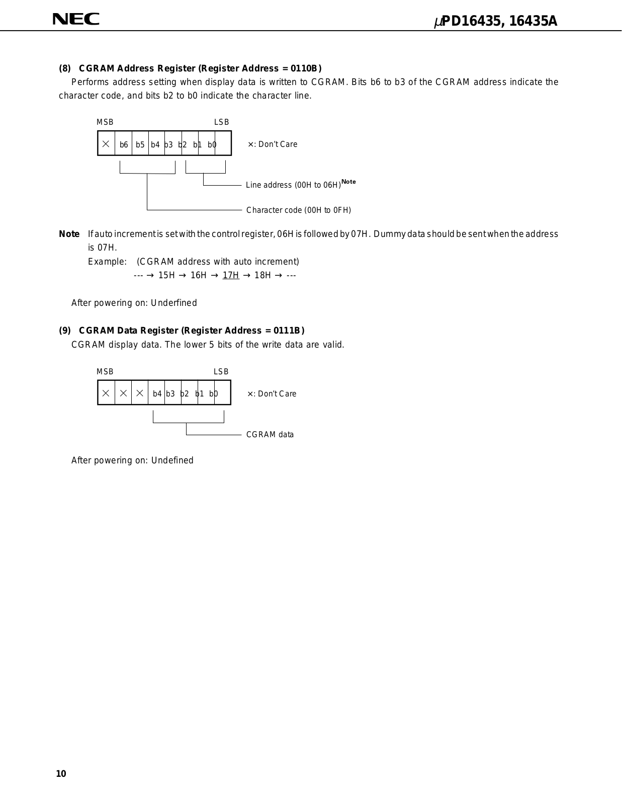
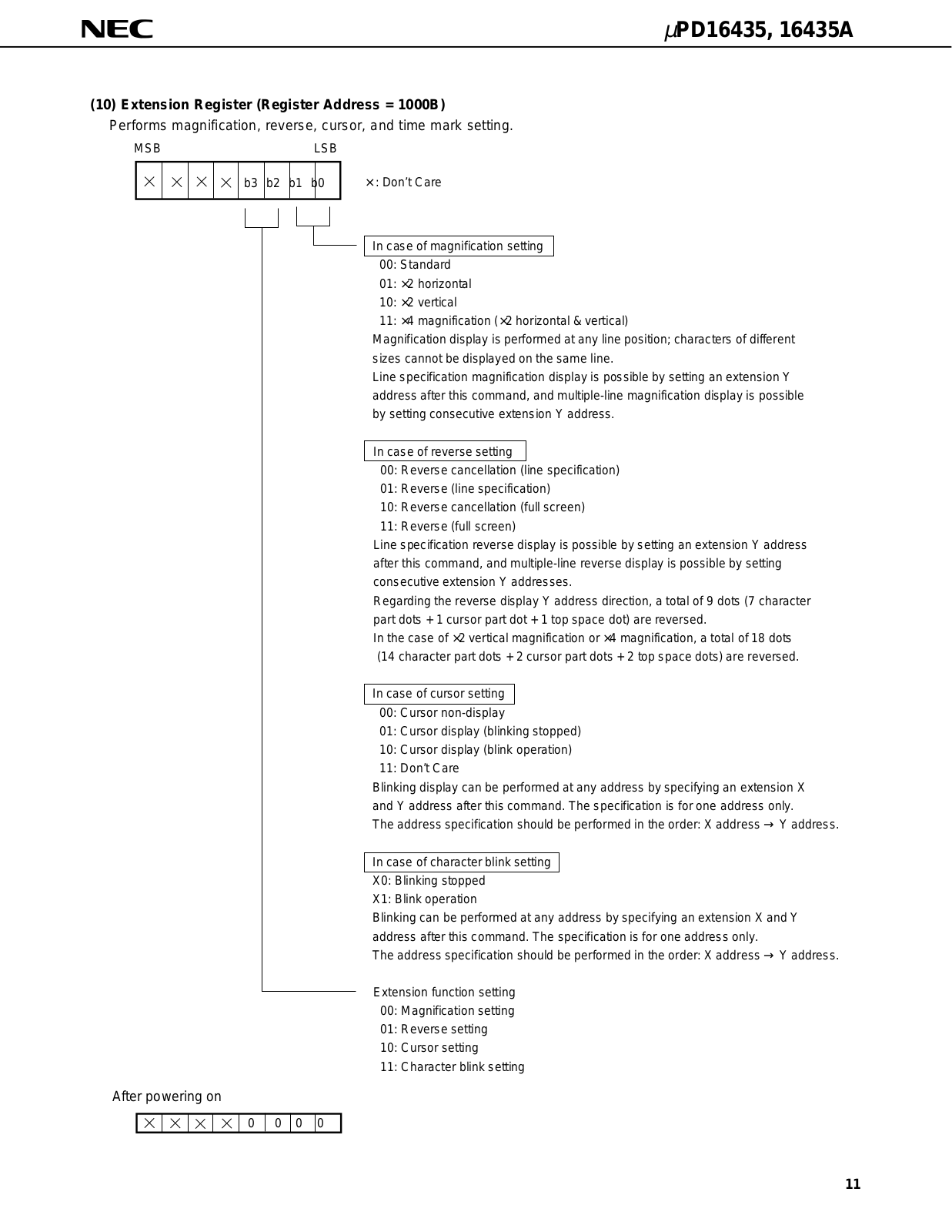
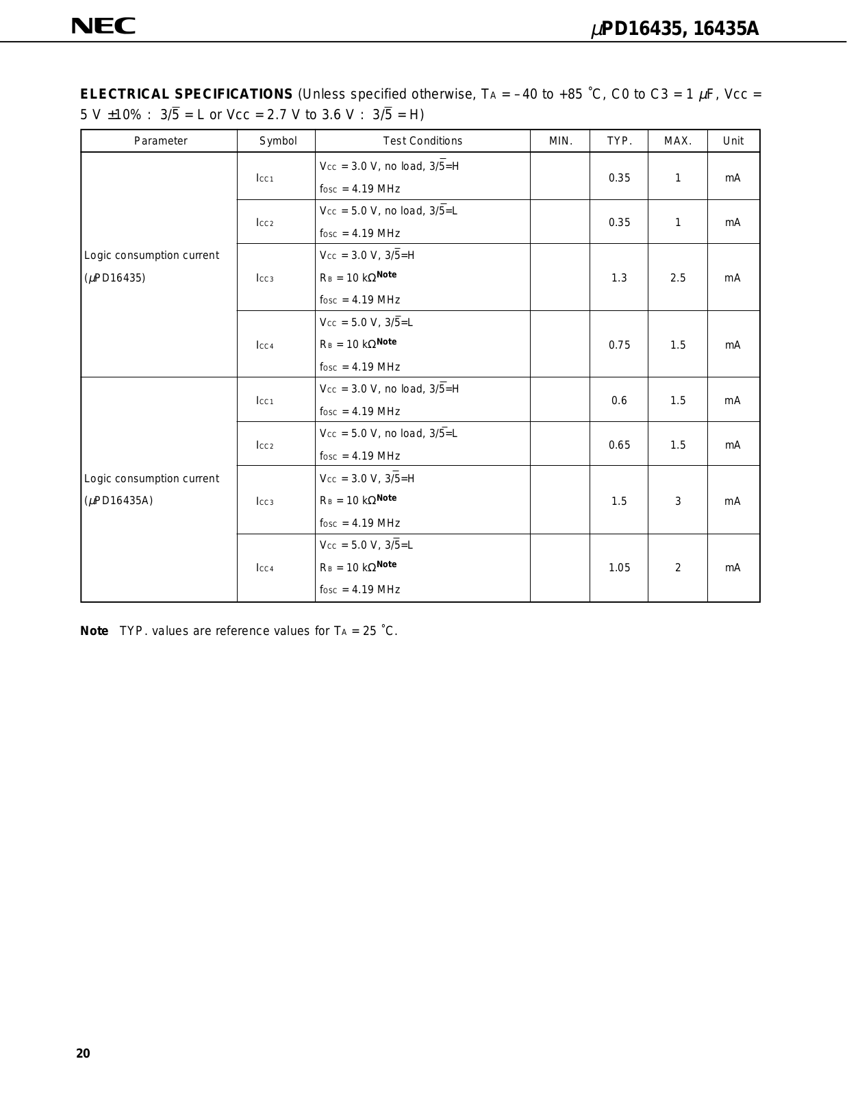
PD16435
PD16435A
PD16647
PD16-73
PD16805
PD168110
PD16855A
PD16855B
PD16855C
PD16855D
PD17071GB-012
PD17072
PD17073
PD178004A
PD178006A
PD178016A
PD178018A
PD17P236
PD17P709A
PD18-12
PD18-73
PD19-73
PD20-0010-S
PD200GB40
PD200GB80
PD200HB120
PD200HB160
PD210
PD22-73
PD23C32000AL
PD23C32340
PD23C32380
PD2401
PD250GB40
PD250GB80
PD250HB120
PD250HB160
PD25F120
PD25F160
PD25F40
PD25F80
PD25GB40
PD25GB80
PD25HB120
PD25HB160
PD2601
PD300F12
PD30CND10NAM5SA
PD30CND10PAM5SA
PD3151F
PD3573
Loading...
Loading...
Nothing found
PD16435
Datasheet (NEC)
36 pgs
288.13 Kb
0
Table of contents
Loading...
Datasheet PD16435, PD16435A Datasheet (NEC)
...
Datasheet Datasheet (NEC)
Download
Specifications and Main Features
Frequently Asked Questions
User Manual
Download
Page 1
Page 2
Page 3
Page 4
Page 5
Page 6
Page 7
Page 8
Page 9
Page 10
Page 11
Page 12
Page 13
Page 14
Page 15
Page 16
Page 17
Page 18
Page 19
Page 20
Page 21
Page 22
Page 23
Page 24
Page 25
Page 26
Page 27
Page 28
Page 29
Page 30
Page 31
Page 32
Page 33
Page 34
Page 35
Page 36
Loading...
+
hidden pages
Unhide
You need points to download manuals.
1 point = 1 manual.
You can buy points or you can get point for every manual you upload.
Buy points
Upload your manuals


")