

Page 1
PRELIMINARY PRODUCT INFORMATION
MOS INTEGRATED CIRCUIT
µµµµ
PD161644A
241 OUTPUT GATE DRIVER WITH POWER SUPPLY FOR TFT-LCD GATE DRIVER
DESCRIPTION
The µPD161644A is a TFT-LCD gate driver with power supply for TFT-LCD driver. Because this gate driver has a
level shift circuit for logic input, it can output a high gate scanning voltage in response to a CMOS-level input. This
ICs can generate the levels which TFT-LCD driver need, from 2.7 V.
FEATURES
• High breakdown voltage output (VDD1–VSS3 = 40 V MAX.)
• 2.7 V CMOS level input
• Number of output: 241 output selectable
• To generate 4 levels from single voltage input
• To integrate regulator circuit for source driver
• Mode setting from source driver: Serial I/F or pin control
• On-chip VCOM driver
• On-chip gate output low-level selector
ORDERING INFORMATION
Part number Package
µ
PD161644A Chip
Remark Purchasing the above chip entails the exchange of documents such as a separate memorandum or
product quality, so please contact one of our sales representatives.
The information contained in this document is being issued in advance of the production cycle for the
device. The parameters for the device may change before final production or NEC Corporation, at its own
discretion, may withdraw the device prior to its production.
Not all devices/types available in every country. Please check with local NEC representative for
availability and additional information.
Document No. S16027EJ0V9PM00 (0.9th edition)
Date Published April 2002 NS CP(K)
Printed in Japan
©
2001
Page 2
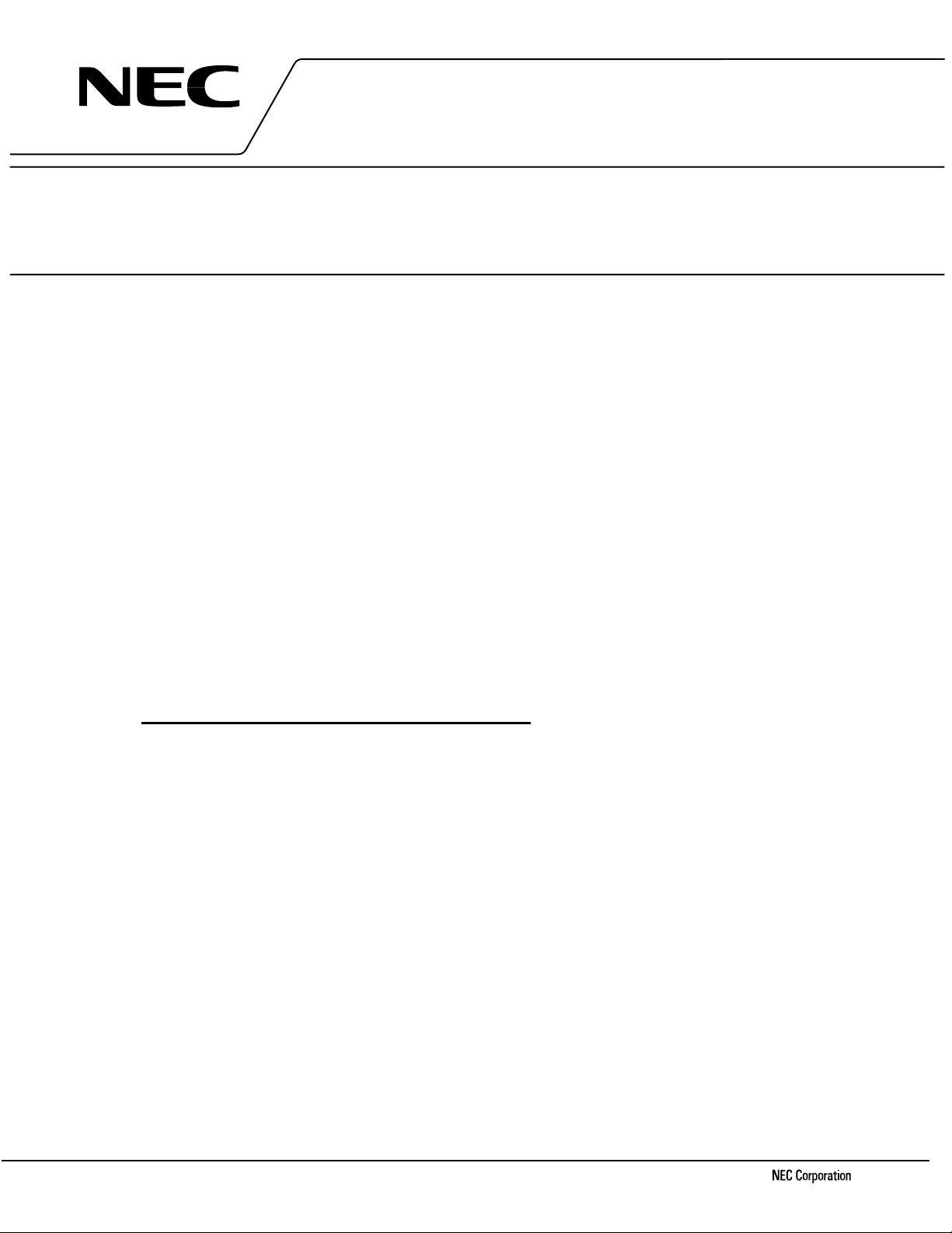
1. BLOCK DIAGRAM/SYSTEM DIAGRAM
C1
C1
C2
C2
C2
C2
C1
C1
C2
C2
C3
C3
C4
C4
C5
C5
C6
C6
DCCLK
GCS
GCL
GDA
DCON
RGONR
VCD2
VMS
FS0
FS2
CLS0
RGON
VSEL
EXRV
ACS0
SCN0
SCN1
SCN2
PUPT0
DUPF0
R,/L
CLK
FRM
STVR
+
-
+
-
+
-
+
-
+
-
+
-
OSC
DC/DC converter
DC/DC converter
DC/DC converter
Serial I/F
register
Switch
SR2SR1
SR120SR119
VREF
D/A
D/A
Gate output
low level select circuit
SR121
SR122
Regurator
R
V
Regurator
R
V
Common
driver
circuit
SR240 SR241
µµµµ
PD161644A
V
DD2
V
DC
C2
V
DD1
C2
V
SS2
C2
V
SS3
C2
V
SS4
V
DC
VGD
V
R
C2
C2
V
S
MVS
VCIN
VCOM
Source driver
C3
5V
4V
Source driver
Common
COMH
C2
COML
C2
VCOMIN
VM
IFSEL
/GRESET
STVL
MPX
OE1
PV
PV
PV
OE2
V
V
V
DC
CC1
SS1
CC1
SS1
SS3
O1O
Level Shifter
2
O
119O120
O
122
O
122
O
O
240
241
VMON
TESTIN1
TESTIN2
TESTOUT1
TESTOUT2
V
B
Remarks 1. /xxx indicates active low signal.
2. Level Shifter (LS): Interfaces between 2.7 V CMOS level and V
2
Preliminary Product Information S16027EJ0V9PM
T to VB level.
Page 3
1.1 Boost Voltage Construction
The boost voltage generated in
µ
PD161644A is shown below.
VGD=VR VGD=VDD2
VDD2 : 5.4V
VDC: 2.7V
VSS1: 0V
VR: 5V
VDD1=VR x 3
=15V
VSS4=VDC x -1
=-2.7V
VSS2=VR x -2
=-10v
VSS3=VR x -3
=-15v
1.2 Boost Voltage Auto Start and Rising Order
VGD=VR, VCD2=H
VDD1=3 x V
R
VDC:2.7V
VSS1:0V
VDD2:5.4V
µµµµ
PD161644A
VDD1=VDD2 x 3
=16.2V
VR:5V
VSS4=VDC x -1
=-2.7V
VSS2=VDD2 x -2
=-10.8V
VSS3=VDD2 x -3
=-16.2V
T1 T2 T3 T4
T1,T2,T3,T4: changeable by PUPT0/1, DUPF0/1
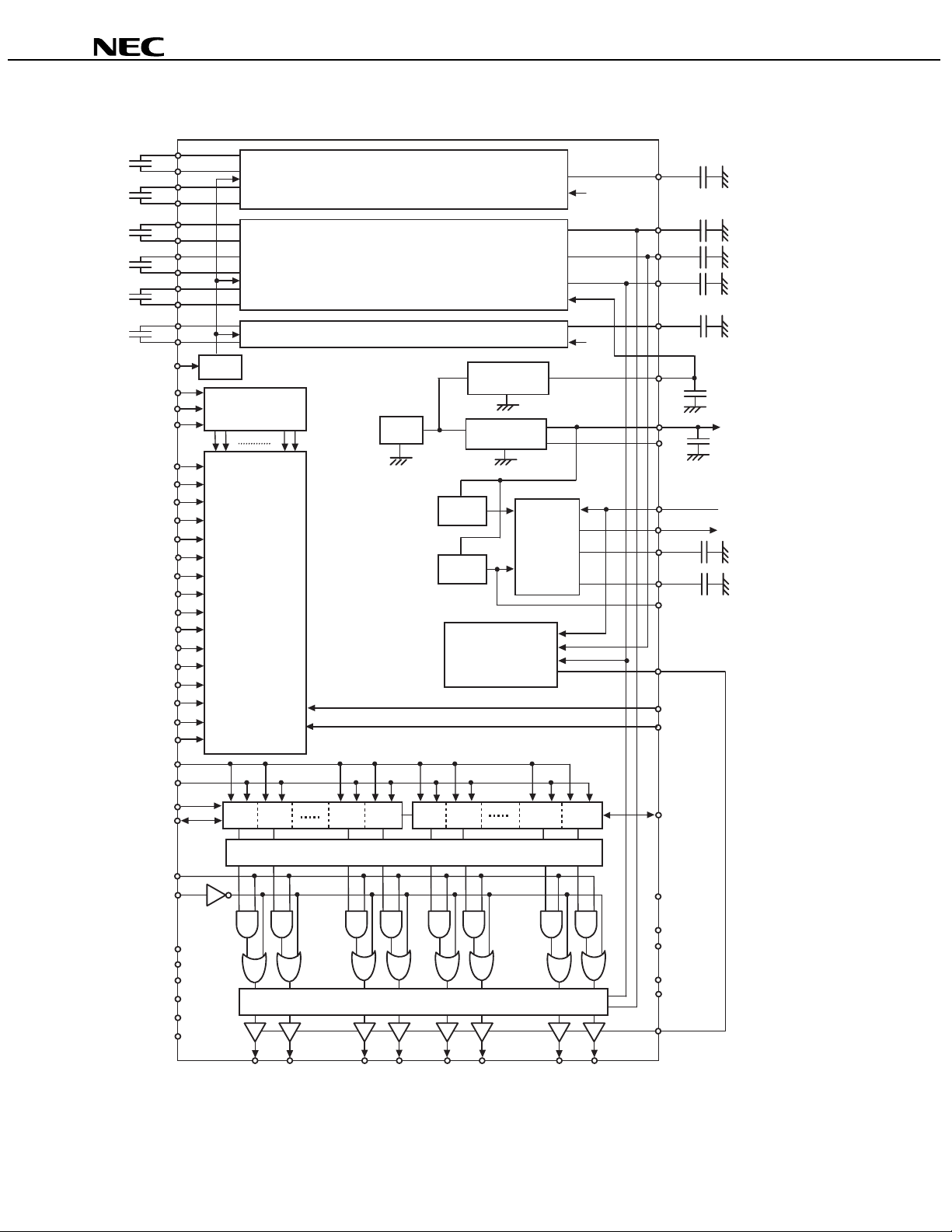
1.3 V
S_AMP Circuit
Vs_AMP circuits are shown below.
TESTOUT1
−
+
RcS
MVS
V
REF
RbS
RaS
VDD2=3 x VDC
VR
DCON
VSS1
VSS4=-VDC
VSS2=-2 x VR
VSS3=-3 x VR
V
DD2
C3
5V
V
S
4V
C3
RbS RaS
MV
S
TESTOUT1
V
REF
−
+
V
DD2
C3
5V
V
S
4V
C3
External Resistor Mode
Internal Resistor Mode
EXRV=L
EXRV=H
RbS
S=(1+ )VREF
V
RaS
Preliminary Product Information S16027EJ0V9PM
3
Page 4
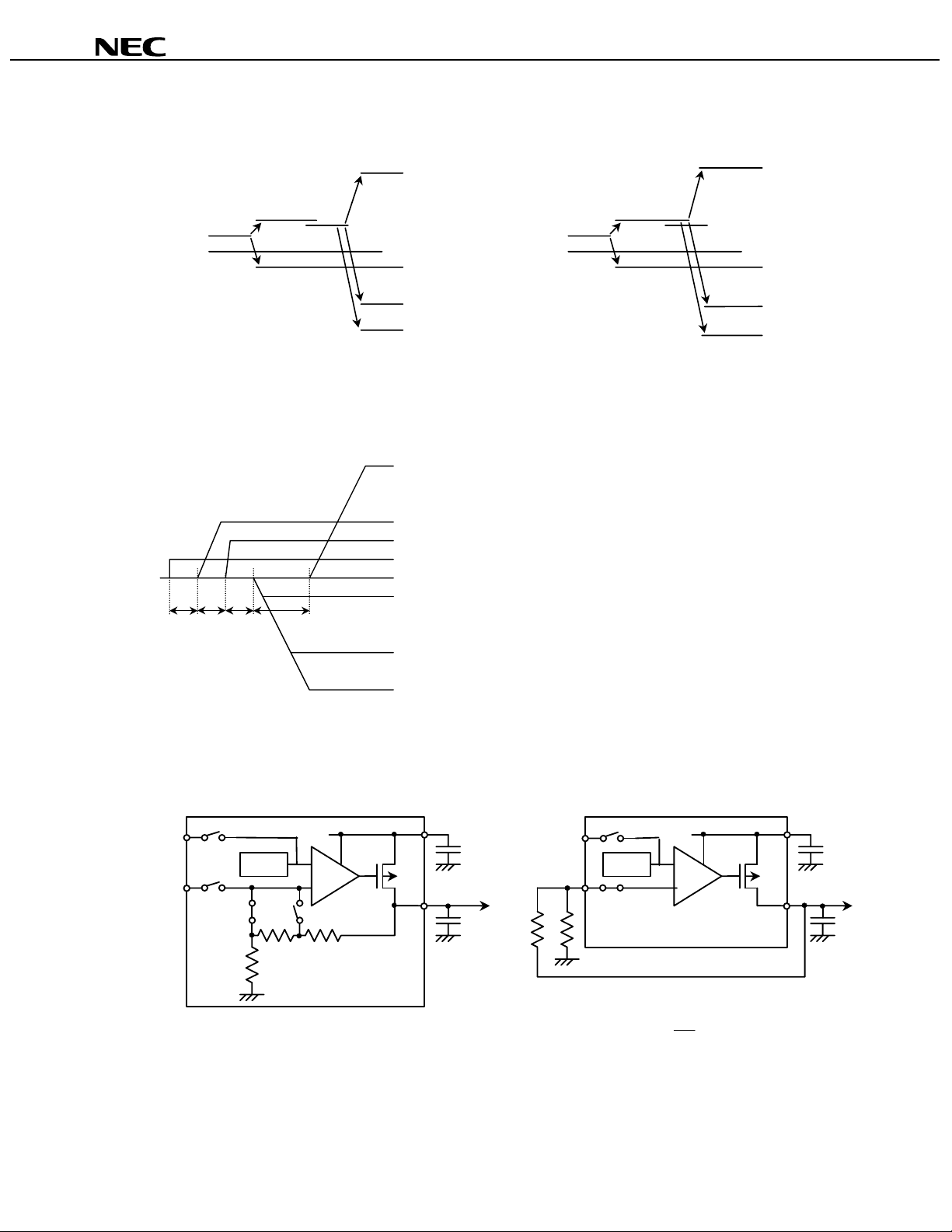
1.4 Common Drive Circuit
The common drive circuit is shown below.
µµµµ
PD161644A
VCOMIN
CDA0
CDA1
CDA2
CDA3
CDA4
CDA5
CDA6
CDA7
DA0
DA1
DA2
DA3
DA4
DA5
DA6
DA7
D/A
VS
D/A
VS
Vs
+
−
Vs
+
−
VDD2
+
−
LS
COMH
C3
VCOM
VCC1
+
−
VSS4
COML
C3
VCIN
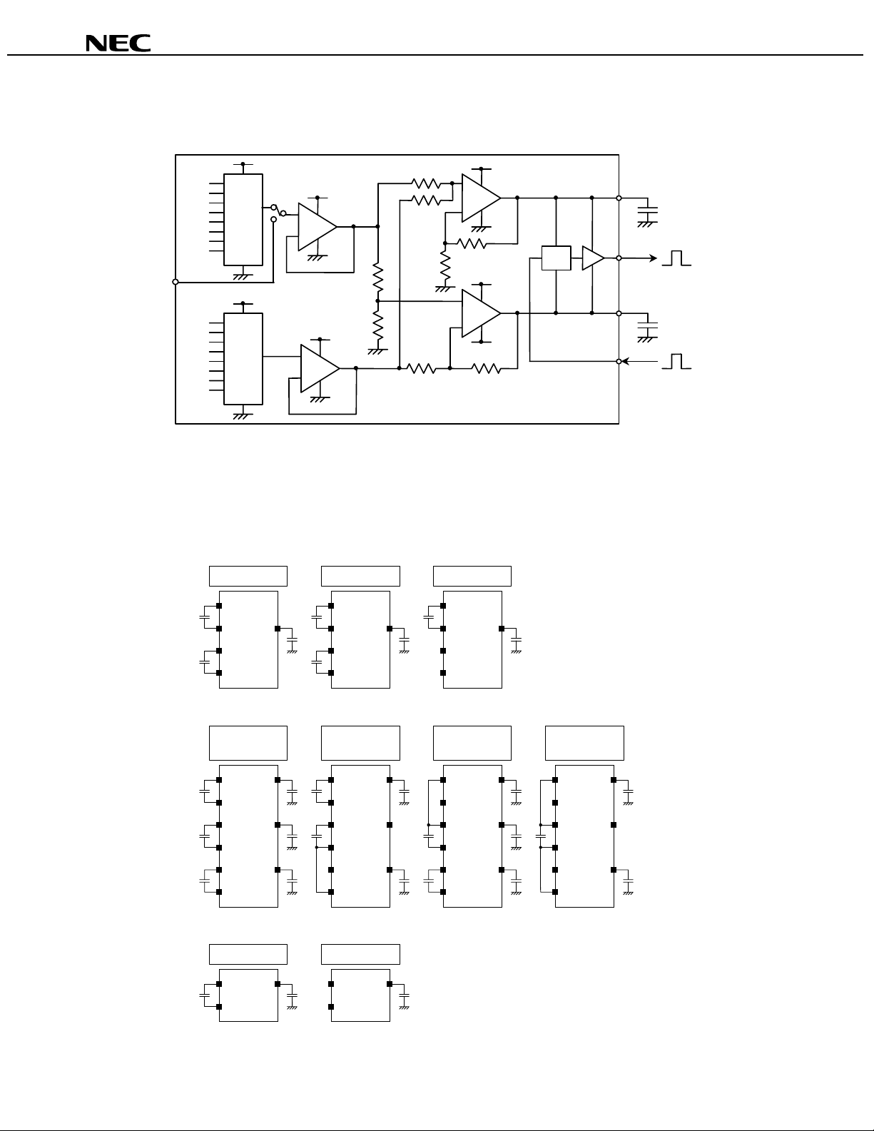
1.5 Variable Boost Steps
The boost steps of VDD1, VSS2, VSS3 are selected according to how the external capacitor is connected.
The examples of connection are shown below. V
between the V
S and VGD pins).
S is selected as a boost reference voltage in these examples (short
VDD2 = VDC x 3
VDD2 = VDC x 2 VDD2 = VDC x 2
(dual mode)
(single mode)
C1+
VDD2
C1-
C2+
C2-
VDD1= VGD x 3
VSS2 = VGD x -2
VSS3 = VGD x -3
C3+
VDD1
C3-
C4+
VSS2
C4-
C5+
VSS3
C5-
VSS4=VDC x -1
+
C6
VSS4
C6-
C1+
C1-
VDD2
C2+
C2-
VDD1= VGD x 3
VSS2 = VSS3 = VGD x -2
C3+
VDD1
C3-
C4+
VSS2
C4-
C5+
VSS3
C5-
VSS4= -
C6+
VSS4
C6-
C1+
VDD2
C1-
C2+
C2-
VDD1= VGD x 2
VSS2 = VGD x -1
VSS3 = VGD x -2
C3+
VDD1
C3-
C4+
VSS2
C4-
C5+
VSS3
C5-
VDD1= VGD x 2
VSS2 = VSS3 = VGD x -1
C3+
VDD1
C3-
C4+
VSS2
C4-
C5+
VSS3
C5-
4
Preliminary Product Information S16027EJ0V9PM
Page 5
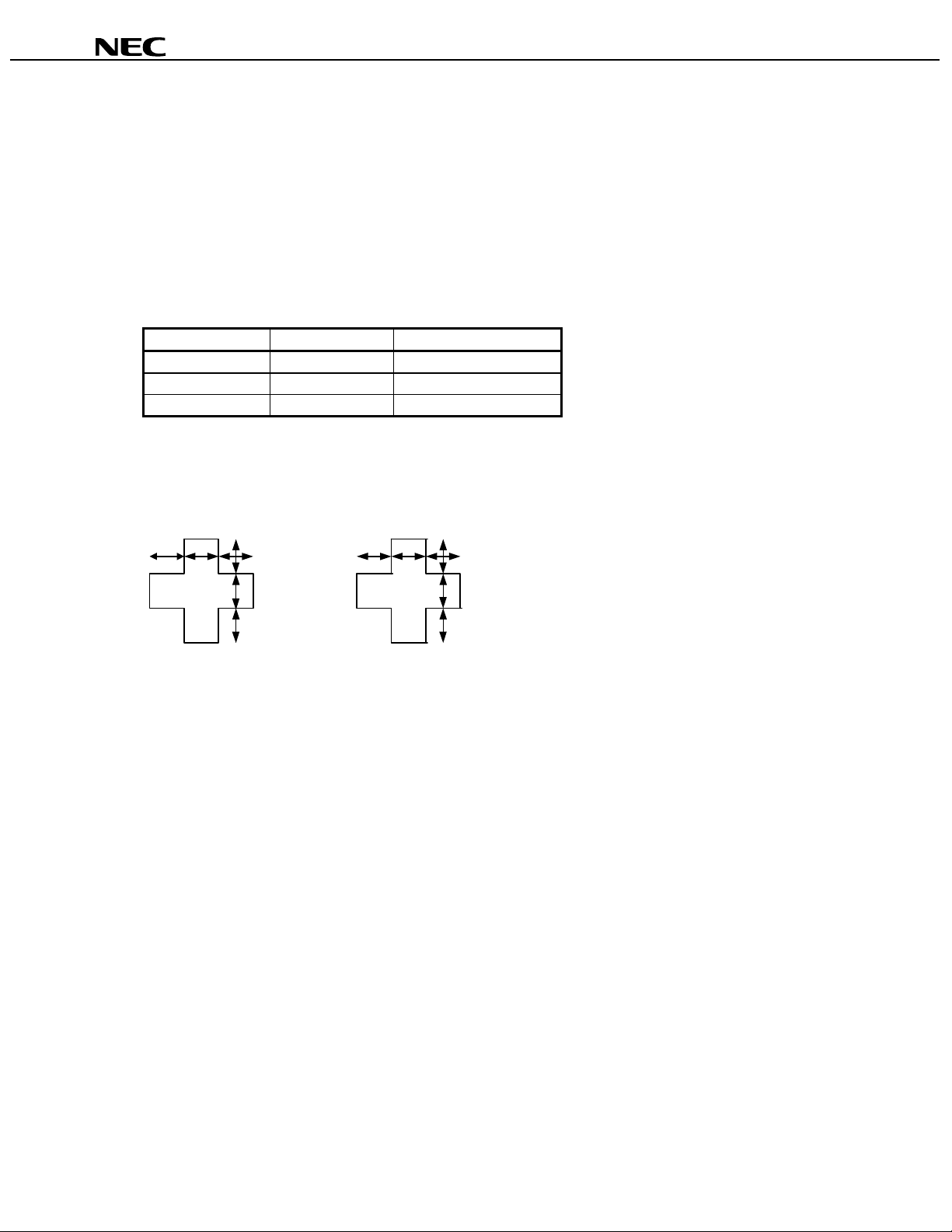
2. PIN CONFIGURATION (Pad Layout)
Chip size: 2.8 mm x 9.4 mm
Bump size
Input/Left/Right (includes DUMMY of input side) : 100
Output (includes DUMMY output side) : 86
Alignment Mark Coordinate (mark center, unit: mm)
X Y Shape of Alignment Mark
−1.125 −4.5705 Type A
0.9705 4.5495 Type B
0.9705 −4.5495 Type B
Alignment Mark
Type A Type B
µ
m x 40 µm
µ
m x 35 µm
µµµµ
PD161644A
10 µm10 µm 10 µm
m
10
µ
µ
m
10
m
10
µ
30 µm30 µm 30 µm
m
30
µ
µ
m
30
m
30
µ
Preliminary Product Information S16027EJ0V9PM
5
Page 6
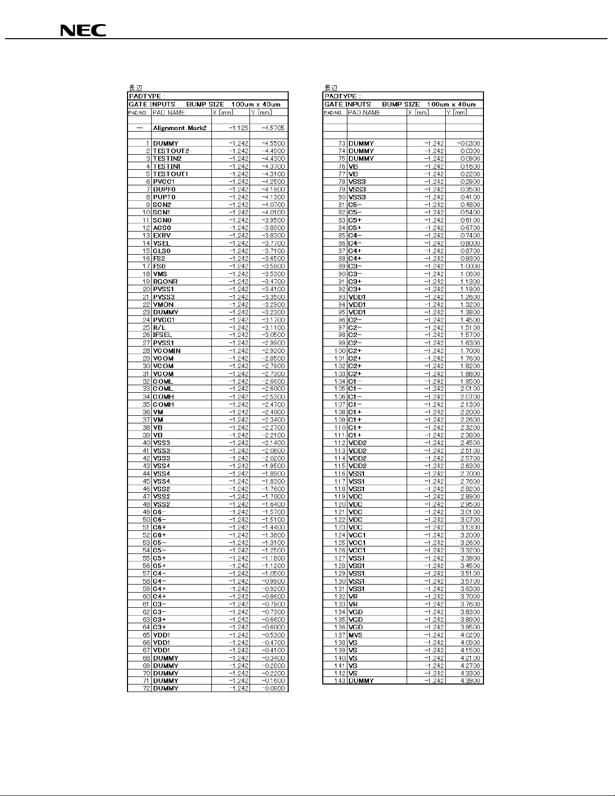
Table 2-1 Pad Layout (1/4)
µµµµ
PD161644A
6
Preliminary Product Information S16027EJ0V9PM
Page 7
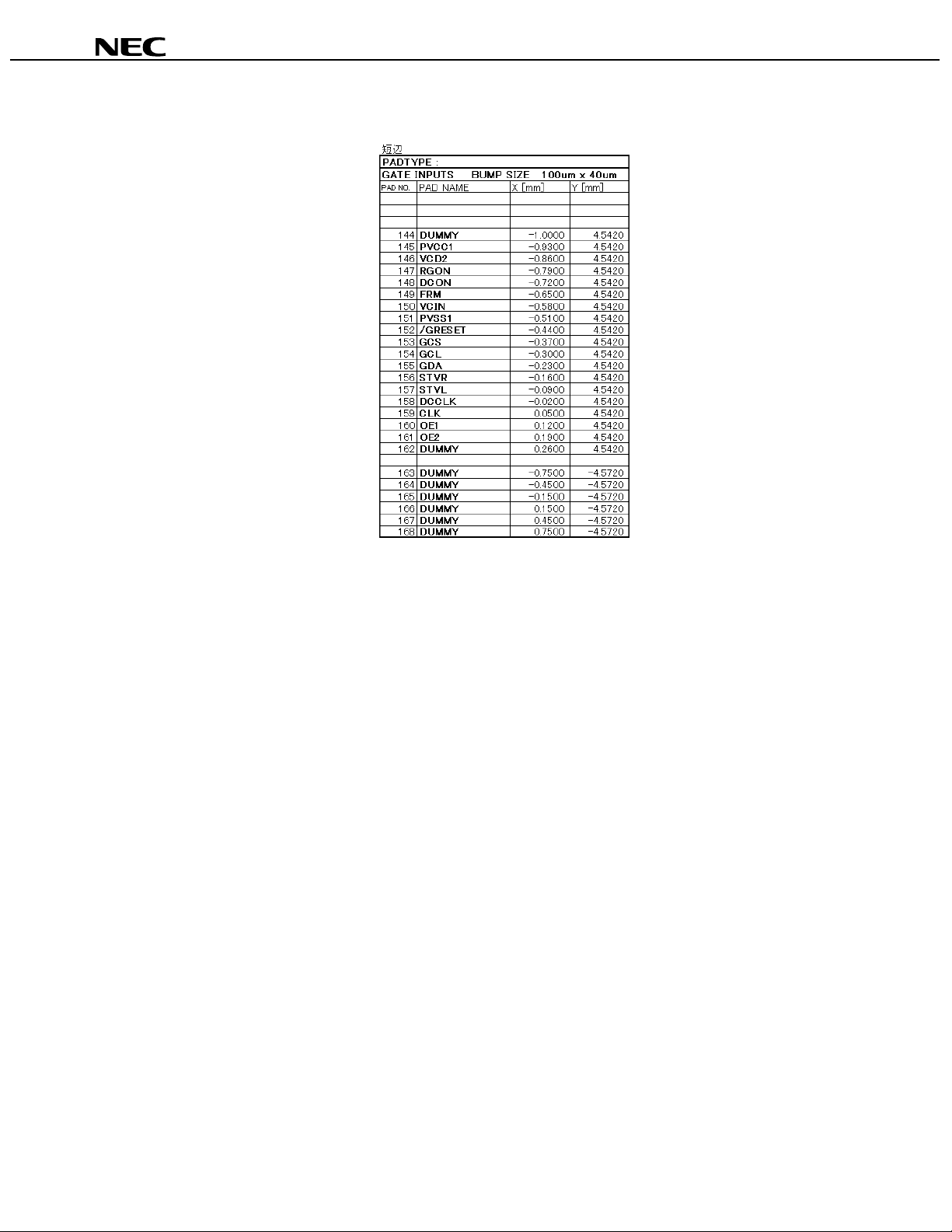
Table 2-1 Pad Layout (2/4)
µµµµ
PD161644A
Preliminary Product Information S16027EJ0V9PM
7
Page 8
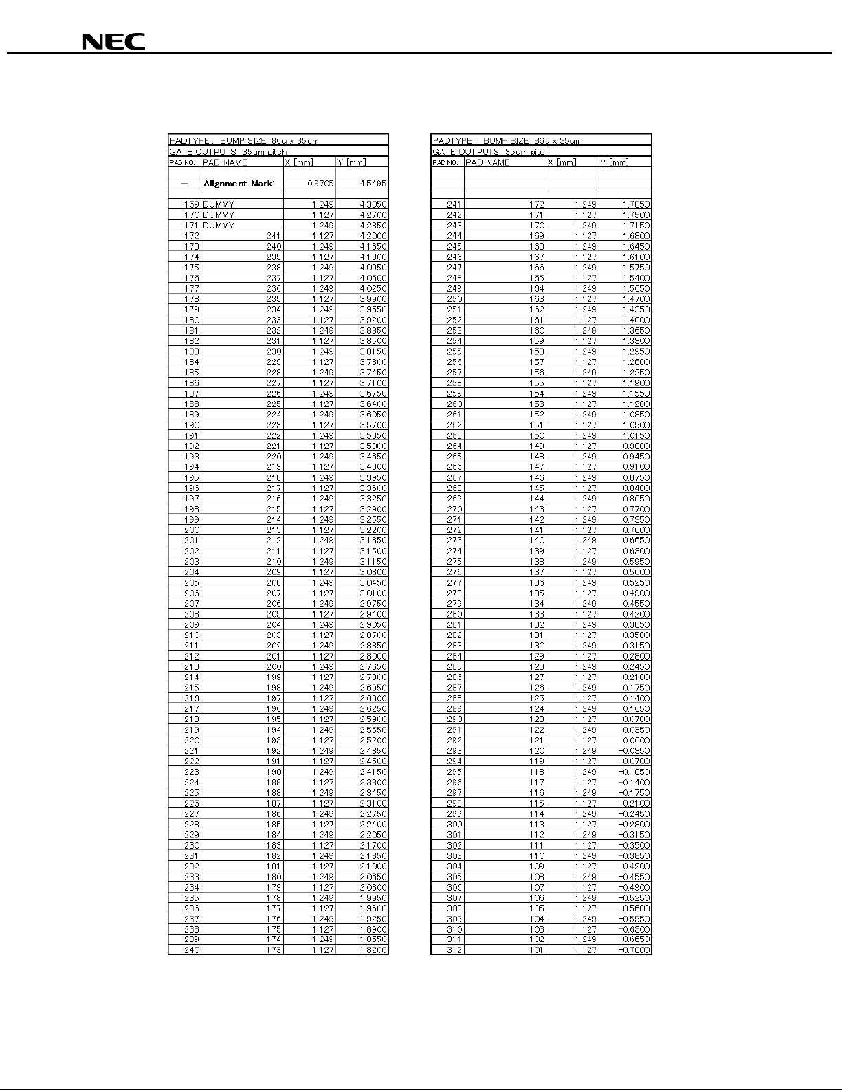
Table 2-1 Pad Layout (3/4)
µµµµ
PD161644A
8
Preliminary Product Information S16027EJ0V9PM
Page 9
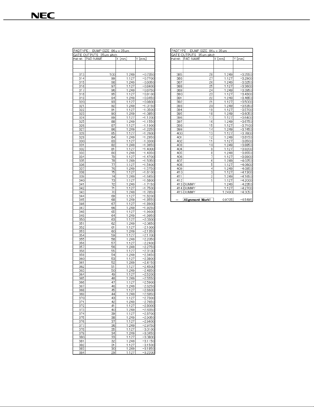
Table 2-1 Pad Layout (4/4)
µµµµ
PD161644A
Preliminary Product Information S16027EJ0V9PM
9
Page 10
µµµµ
PD161644A
3. PIN FUNCTIONS
Symbol Pin Name Pad No. I/O Function
O1 to O241 Driver output pins 388 to 148 Output Scan signal output pins that drive the gate electrode of a TFT-
LCD.
The status of each output pin changes in synchronization with
the rising edge of shift clock CLK. The output voltage of the
driver is V
CLK Shift clock input 139 Input Shift clock input for the internal shift resistor. The contents of
internal shift resistor are shifted at the rising edge of CLK.
Connect to GCLK pin of source driver.
STVR,
STVL
OE1 Enable input 140 Input If the level selected by OE1SEL is input, the driver output is
OE2 Enable input 141 Input If the level selected by OE2SEL is input, the driver output is
R,/L Shift direction
FRM Frame signal
GCS Chip select input 133 Input <IFSEL = 0> To input chip select signals.
GCL Serial clock input 134 Input <IFSEL = 0> To input serial clock signals.
Start pulse
input/output pin
switching
input
input
136,
137
25 Input Shift direction switching input pin of the internal shift register.
129 Input Input frame reverse signals.
I/O Input/output pin of the internal shift resistor.
Start pulse signal (output from GSTB pin of source driver) is
read at the rising edge of shift clock CLK and a scan signal is
output from the driver output pin.
The valid level of the STVR/STVL pin is determined by the
setting of STVSEL.
When STVSEL = L, the pulse becomes low level at the falling
edge of the 240th shift clock CLK and high level at falling
edge of the 241st clock.
fixed to low level. (When OE1SEL = L the driver output is fixed
to low level if a low level is input.)
However, the shift resistor is not cleared. And, output enable
actuation is asynchronous in the clock.
Connect to GOE1 pin of source driver.
fixed to high level. (When OE2SEL = L the driver output is fixed
to low level if a high level is input.)
However, the shift resistor is not cleared. And, output enable
actuation is asynchronous in the clock.
Connect to GOE2 pin of source driver.
R,/L = 1 (right shift): STVR →O
R,/L = 0 (left shift): STVL →O
Connect to GFRAME pin of source driver.
Connect to GCS pin of source driver.
<IFSEL = 1> Leave open.
Connect to GCL pin of source driver.
<IFSEL = 1> Leave open.
DD1 to VB.
1 →O2 ··· O239 →O240 →STVL
241 →O240 ··· O2 →O1 →STVR
(1/5)
10
Preliminary Product Information S16027EJ0V9PM
Page 11
µµµµ
PD161644A
Symbol Pin Name Pad No. I/O Function
GDA Serial data input 135 Input <IFSEL = 0> To input serial data signals.
Connect to GDA pin of source driver.
<IFSEL = 1> Leave open.
/GRESET Reset input 132 Input Reset input pin. Connect to /GRESET pin of source driver.
If /GRESET is made low, the serial interface is initialized (the
register values are not initialized). A reset operation is
executed according to the level of the /GRESET signal. Be
sure to execute a reset using this pin at power application.
VCIN Common pulse
input
DCCLK Clock input for
DC/DC converter
130 Input To input common pulse. Connect to VCOUT3 pin of source
driver. Fix this pin to low when not using it.
138 Input To input the external clock for the DC/DC converter.
This pin is valid only when CLS0 = 1 and CLS1 = 1. Other
settings cause this pin to be pulled down to low level, so in
these cases, leave open.
VGD Power supply input
for DC/DC
114 to 116 Input Reference voltage input pins for V
Connect to any of V
DD2, VR or VS.
DD1, VSS1 to VSS4 boost.
converter
VR Power supply
output for DC/DC
converter
VS Positive power
output supply for
111 to 113 Output Positive power supply voltage output for the DC/DC converter.
R output voltage can be changed by setting VRSEL0 to
The V
VRSEL2.
118 to 123 Output Positive power supply voltage output for source driver. The V
output voltage can be changed by setting VSEL0 to VSEL2.
driver
MVS External resistor
input
117 Input Any output voltage can be set by connecting an external
resistor.
<EXRV = 0> Leave open.
<EXRV = 1> Connect to external resistor.
−
C1 +, C1
C2 +, C2
C3 +, C3
C4 +, C4
C5 +, C5
C6 +, C6 −
VDD1 DC/DC converter
Capacitor connect
−
pin for boost
−
−
−
output
80 to 83, 76 to 79,
72 to 75, 68 to 71,
63, 64, 61, 62,
59, 60, 57, 58,
55, 56, 53, 54,
− To connect booster for DC/DC converter.
The recommended values of the capacitance and tolerance of
each capacitor are shown below.
µ
Capacitance : C1, C2: 1
F, C3 to C6: 0.47 µF
Tolerance : 10 V
51, 52, 49, 50
65 to 67 Output Boost voltage of DC/DC converter (VR x2 or x3).
The boost step number of V
DD1 is selected according to how
the external capacitor is connected. The boost reference
voltage can be set using VGD. Refer to the function of VGD
pin.
VDD2 DC/DC converter
output
VSS2 DC/DC converter
output
84 to 87 Output Boost voltage of DC/DC converter (VDC x2 or x3). The boost
step number for V
DD2 can be set using VCD2.
46 to 48 Output Boost voltage of DC/DC converter (VR x-1 or x-2).
The boost step number of V
SS2 is selected according to how the
external capacitor is connected. The boost reference voltage
can be set using VGD. Refer to the function of VGD pin.
(2/5)
S
Preliminary Product Information S16027EJ0V9PM
11
Page 12
µµµµ
PD161644A
Symbol Pin Name Pad No. I/O Function
VSS3 DC/DC converter
output
40 to 42, 143 Output Boost voltage of DC/DC converter (VR x-1 or x-2).
The boost step number of V
SS2 is selected according to how
the external capacitor is connected. The boost reference
voltage can be set using VGD. Refer to VGD pin function.
VSS4 DC/DC converter
43 to 45 Output Boost voltage output of DC/DC converter (VDC x-1).
output
COMH Common high level
output
34, 35 Output <COMON = 1> High level of common voltage is output. The
voltage level changes accordance with DA0 to DA7 and CDA0
to CDA7.
<COMON = 1> Leave open when not using it.
COML Common low
level output
32, 33 Output <COMON = 1> Low level of common voltage is output. The
voltage level changes accordance with DA0 to DA7 and CDA0
to CDA7.
<COMON = 0> Leave open when not using it.
VCOM Common output 29 to 31 Output <COMON = 1> The common voltage synchronized with the
VCIN input is output.
Connect to common pin of panel.
<COMON = 0> Leave open when not using it.
VM Gate output low
level select
36, 37 Output Gate output low level select voltage synchronized with the
VCIN input is output. Connect to V
B pin.
voltage
VB Driver negative
voltage
38, 39 Input Negative voltage of output buffer. This is the input pin of the
liquid crystal driver negative voltage. Connect to V
M pin.
IFSEL I/F selection 26 Input The serial I/F input switching pin.
<IFSEL = 0> Serial I/F input.
The DCON, RGONR, VCD2, VMS, FS0, FS2, CLS0, RGON,
VSEL, EXRV, ACS0, SCN0, SCN0, SCN2, PUPT0, DUPF0
pins should be left open.
<IFSEL = 1> Control pin input.
The GCS, GCL, GDA pins should be left open.
DCON DC/DC converter
control
128 Input <IFSEL = 0> Leave open. (Internal resistors are valid.)
<IFSEL = 1> The DC/DC converter ON/OFF control signal is
input. Connect to the DCON pin of the source driver.
<DCON = 0> DC/DC converter OFF.
<DCON = 1> DC/DC converter ON.
RGONR VR regulator
control
VCD2 VDD2 boost
selection
19 Input <IFSEL = 0> Leave open. (Internal resistors are valid.)
<IFSEL = 1> The V
<RGONR = 0> V
<RGONR = 1> V
R regulator ON/OFF control signal is input.
R regulator OFF.
R regulator ON.
126 Input <IFSEL = 0> Leave open. (Internal resistors are valid.)
<IFSEL = 1> The V
<VCD2 = 0> V
<VCD2 = 1> V
DD2 boost step number select pin.
DD2 = VDC x 2.
DD2 = VDC x 3.
(3/5)
12
Preliminary Product Information S16027EJ0V9PM
Page 13
Symbol Pin Name Pad No. I/O Function
VMS VDD2 boost
selection
VCOMIN VCOM center
voltage input
18 Input <IFSEL = 0> Leave open. (Internal resistors are valid.)
<IFSEL = 1> V
<VMS = 0> V
<VMS = 1> V
DD2 boost mode select pin.
DD2: single boost mode
DD2: dual boost mode
28 Input VCOM center voltage input pin.
Leave open when COMSEL = 0.
<COMSEL = 0> Internal D/A is valid.
<COMSEL = 1> VCOMIN input voltage is valid.
FS0 VDD2 boost
frequency
selection in scan
17 Input <IFSEL = 0> Leave open. (Internal resistors are valid.)
<IFSEL = 1> V
<FS0 = 0 > f
DD2 boost frequency select pin in scan mode
OSC/2 <FS0 = 0 > fOSC/4
mode
FS2 VDD1, VSS2 to
SS4 boost
V
frequency
selection in scan
16 Input <IFSEL = 0> Leave open. (Internal resistors are valid.)
<IFSEL = 1> V
DD1, VSS2 to VSS4 boost frequency select pin in
scan mode.
<FS2 = 0 > f
OSC/2 <FS2 = 1, > fOSC/4
mode
CLS0 DC/DC OSC
frequency
selection
15 Input <IFSEL = 0> Leave open. (Internal resistors are valid.)
<IFSEL = 1> Select pin of the OSC oscillation frequency for
DC/DC converter.
<CLS0 = 0> f
OSC = 20 kHz, DCCLK: Open
<CLS0 = 1> External CK input mode
RGON VS regulator
control
127 Input <IFSEL = 0> Leave open. (Internal resistors are valid.)
<IFSEL = 1> The V
S regulator ON/OFF control signal is input.
Connect this pin to the RGON pin of the source driver.
S regulator OFF.
S regulator ON.
S = 4 V
S = 5 V
VSEL VS regulator voltage
selection
EXRV VS regulating
resistor
selection
<RGON = 0> V
<RGON = 1> V
14 Input <IFSEL = 0> Leave open. (Internal resistors are valid.)
<IFSEL = 1> Select pin of output voltage for V
<VSEL = 1> V
<VSEL = 0> V
13 Input <IFSEL = 0> Leave open. (Internal resistors are valid.)
<IFSEL = 1> Select pin of external resistor for V
<EXRV = 0> Internal resistor setting mode.
<EXRV = 1> Any output voltage can be set by connecting
MVS to an external resistor
ACS0
Amp. current
selection in scan
mode
12 Input <IFSEL = 0> Leave open. (Internal resistors are valid.)
<IFSEL = 1> Amp. current select pin in scan mode.
<ACS0 = 0> Amp. current = 5
<ACS0 = 1> Amp. current = 15
µµµµ
PD161644A
(4/5)
S regulator.
S regulator.
µ
A.
µ
A
Preliminary Product Information S16027EJ0V9PM
13
Page 14
Symbol Name Pad No. I/O Function
SCN0,
SCN1,
SCN2
PUPT0 Setting pin of
DUPF0 Operating
VMON Stand-by current
TESTOUT1 VREF reference
VDC DC/DC converter
VCC1 Logic reference
VSS1 Ground 105 to 110 − Connect to the system ground.
PVCC1 Pull-up voltage 6, 24, 125 − Pull-up voltage for mode setting pins.
PVSS1 Pull-down voltage 20, 27, 131 − Pull-down voltage for mode setting pins.
TESTIN1,
TESTIN2
TESTOUT2 TEST output pin 2 Output Test output pin. Leave open.
PVSS3 Pull-down voltage 21 − Pull-down voltage for mode setting pin.
DUMMY Dummy 1, 23, 92, 124,
Gate scan
selection
DC/DC converter
power on time
frequency setting
pin at DC/DC
converter power
on
reduction control
pin
voltage output
reference voltage
voltage
TEST input pin 4,
11,
10,
9
8 Input <IFSEL = 0> Leave open. (Internal resistors are valid.)
7 Input <IFSEL = 0> Leave open. (Internal resistors are valid.)
22 Input The standby current reduction control pin.
5 Output The VREF voltage measurement pin.
93 to 100 − Reference voltage input pin for DC/DC converter.
101 to 104 − 2.7 V ± 5% LS: level shifter reference voltage input pins.
3
142, 144 to 147,
389 to 391
Input <IFSEL = 0> Leave open. (Internal resistors are valid.)
<IFSEL = 1> Select pin of Gate scan order.
<SCN0 = 1, SCN1 = 1, SCN2 = 1> MODE1
<SCN0 = 1, SCN1 = 1, SCN2 = 0> MODE2
<SCN0 = 1, SCN1 = 0, SCN2 = 1> MODE3
<SCN0 = 1, SCN1 = 0, SCN2 = 0> MODE4
<SCN0 = 0, SCN1, SCN2 = x> MODE5
<IFSEL = 1> This pin sets the rising time of V
SS4 at DC/DC converter power on time.
to V
<IFSEL = 1> This pin sets the operating frequency at DC/DC
converter power on time.
<DUPT0 = 0> f
<DUPT0 = 0> f
<VMON = PVSS3> Normal mode
A quiescent current of about 0.5
mode. When the V
are fixed to ALL-High.
<VMON = PVCC1> Standby current reduction mode
Makes the quiescent current consumed in standby mode 0.
When the V
undefined.
Leave open.
Input Test input pins. Leave open.
− Dummy data
OSC/8
OSC/16
µ
A is consumed in standby
CC1 voltage drops, the driver output pins
CC1 voltage drops, the driver output pins are
µµµµ
PD161644A
(5/5)
DD1, VDD2, VSS2
14
Preliminary Product Information S16027EJ0V9PM
Page 15
µµµµ
PD161644A
4. COMMAND
4.1 Command List
Data bit
7 6 5 4 3 2 1 0 Register 7 6 5 4 3 2 1 0
0 0 0 1 1 0 0 0 R24 DC/DC operation
setting
0 0 0 1 1 0 0 1 R25 DC/DC step setting VRSEL2 VRSEL1 VRSEL0 VMS VCD2
0 0 0 1 1 0 1 0 R26 DC/DC oscillation
setting
0 0 0 1 1 0 1 1 R27 Regulator output setting ACS1 ACS0 EXRV VSEL2 VSEL1 VSEL0 RGON
0 0 0 1 1 1 0 0 R28 LPM setting LACS1 LACS0 LFS3 LFS2 LFS1 LFS0 LPM
0 0 0 1 1 1 0 1 R29 Gate scan setting OE2SELOE1SELSTVSEL SCN2 SCN1 SCN0
0 0 0 1 1 1 1 0 R30 Gate mode setting COMHI COMSEL COMON NLINE2 NLINE1
0 0 0 1 1 1 1 1 R31 Common amplitude
setting
0 0 1 0 0 0 0 0 R32 Common center setting CDA7 CDA6 CDA5 CDA4 CDA3 CDA2 CDA1 CDA0
0 0 1 0 0 0 0 1 R33 DC/DC power on setting PONM PON DUPF1 DUPF0 PUPT1 PUPT0
0 0 1 0 0 0 1 0 R34 Reset RES
RGONR VS4ON VS3ON VS2ON VD2ON VD1ON DCON
FUP CLS1 CLS0 FS3 FS2 FS1 FS0
DA7 DA6 DA5 DA4 DA3 DA2 DA1 DA0
4.2 Command Description
Reset the internal data at power application by inputting a low level to the /GRESET pin.
(1/3)
Resistor Bit Symbol Reset Functions Descriptions
R24 D0 DCON 0 DC/DC converter control Control ON/OFF of DC/DC converter
<DCON = 0> DC/DC converter OFF
<DCON = 1> DC/DC converter ON
D1 VD1ON 0 VDD1 boost control Control ON/OFF of VDD1 boost
<VD1ON = 0> V
<VD1ON = 1> V
D2 VD2ON 0 VDD2 boost control Control VDD2 boost ON/OFF
<VD2ON = 0> V
<VD2ON = 1> V
D3 VS2ON 0 VSS2 boost control Control VSS2 boost ON/OFF.
<VS2ON = 0> V
<VS2ON = 1> V
D4 VS3ON 0 VSS3 boost control Control VSS3 boost ON/OFF.
<VS3ON = 0> V
<VS3ON = 1> V
D5 VS4ON 0 VSS4 boost control Control VSS4 boost ON/OFF.
<VS4ON = 0> V
<VS4ON = 1> V
D6 RGONR 0 VR regulator control Control ON/OFF of VR regulator
<RGON = 0> V
<RGON = 1> V
DD1 boost OFF
DD1 boost ON
DD2 boost OFF
DD2 boost ON
SS2 boost OFF
SS2 boost ON
SS3 boost OFF
SS3 boost ON
SS4 boost OFF
SS4 boost ON
R regulator OFF
R regulator ON
Preliminary Product Information S16027EJ0V9PM
15
Page 16

Resistor Bit Symbol Reset Functions Descriptions
R25 D0 VCD2 0 VDD2 boost selection Select the number of VDD2 boost step (x2/x3)
<VCD2 = 0> V
DD2 = VDC x 2
<VCD2 = 1> VDD2 = VDC x 3
D1 VMS 1 VDD2 boost mode
D2
D3
D4
VRSEL0
VRSEL1
VRSEL2
selection
1
0
V
voltage selection
1
R regulator output
Select VDD2 boost mode
<VMS = 0> V
<VMS = 1> V
DD2 = Single boost mode
DD2 = Dual boost mode
Select output voltage of VR regulator. When IFSEL = 1,
V
R is fixed to 5 V.
<VRSEL0 = 0, VRSEL1 = 0, VRSEL2 = 0> V
<VRSEL0 = 1, VRSEL1 = 0, VRSEL2 = 0> V
<VRSEL0 = 0, VRSEL1 = 1, VRSEL2 = 0> V
<VRSEL0 = 1, VRSEL1 = 1, VRSEL2 = 0> V
<VRSEL0 = 0, VRSEL1 = 0, VRSEL2 = 1> V
<VRSEL0 = 1, VRSEL1 = 0, VRSEL2 = 1> V
<VRSEL0 = 0, VRSEL1 = 1, VRSEL2 = 1> V
<VRSEL0 = 1, VRSEL1 = 1, VRSEL2 = 1> V
R26 D0
D1
D2
D3
D4
D5
FS0
FS1
FS2
FS3
CLS0
CLS1
1
0
1
0
1
0
VDD2 boost frequency
selection in scan mode
VDD1, VSS2 to VSS4
boost frequency
selection in scan mode
DC/DC OSC frequency
selection
Select VDD2 boost frequency in scan mode. When
IFSEL = 1, FS1 is fixed to 0.
<FS0 = 0, FS1 = 0> f
<FS0 = 0, FS1 = 1> f
Select V
mode.
DD1, VSS2 to VSS4 boost frequency in scan
When IFSEL = 1, FS3 is fixed to 0.
<FS2 = 0, FS3 = 0> f
<FS2 = 0, FS3 = 1> f
OSC/2 <FS0 = 1, FS1 = 0> fOSC/4
OSC/8 <FS0 = 1, FS1 = 1> fOSC/16
OSC/2 <FS2 = 1, FS3 = 0> fOSC/4
OSC/8 <FS2 = 1, FS3 = 1> fOSC/16
Select oscillation frequency of OSC for DC/DC
converter. When IFSEL = 1, CLS1 is fixed to 1
<CLS0 = 0, CLS1 = 0> f
<CLS0 = 1, CLS1 = 0> f
<CLS0 = 0, CLS1 = 1> f
OSC = 15 KHz, DCCLK: Open
OSC = 20 KHz, DCCLK: Open
OSC = 30 KHz, DCCLK: Open
<CLS0 = 1, CLS1 = 1> External CK input mode
D6 FUP 0 Switching of DC/DC
OSC frequency
Select oscillation frequency of OSC for DC/DC
converter. When IFSEL = 1, the frequency is fixed to
f
OSC.
<FUP = 0> f
<FUP = 1> f
OSC
OSC x 2
µµµµ
PD161644A
(2/3)
R = 3 V
R = 3.5 V
R = 4 V
R = 4.5 V
R = 4.75 V
R = 5 V
R = 5.25 V
R = 5.5 V
16
Preliminary Product Information S16027EJ0V9PM
Page 17

Resistor Bit Symbol Reset Functions Descriptions
R27 D0 RGON 0 VS regulator control Control ON/OFF of VS regulator
D1
D2
D3
VSEL0
VSEL1
VSEL2
1
0
1
V
S regulator output
voltage selection
<RGON = 0> V
<RGON = 1> V
Select the output voltage of VS regulator.
VSEL0 = 0: V
<VSEL0 = 0, VSEL1 = 0, VSEL2 = 0> V
S regulator OFF
S regulator ON
S = 5 V, VSEL = 1, VS = 4 V when IFSEL = 1.
<VSEL0 = 1, VSEL1 = 0, VSEL2 = 0> V
<VSEL0 = 0, VSEL1 = 1, VSEL2 = 0> V
<VSEL0 = 1, VSEL1 = 1, VSEL2 = 0> V
<VSEL0 = 0, VSEL1 = 0, VSEL2 = 1> V
<VSEL0 = 1, VSEL1 = 0, VSEL2 = 1> V
<VSEL0 = 0, VSEL1 = 1, VSEL2 = 1> V
<VSEL0 = 1, VSEL1 = 1, VSEL2 = 1> V
D4 EXRV 0 VS regulator resistor
selection
Select external resistor of VS regulator.
<EXRV = 0> Internal resistor mode
<EXRV = 1> Connect external resistor to MVS and set
D5
D6
ACS0
ACS1
0
Amp. current selection
0
in scan mode
any level of voltage
Select Amp. current of VR and VS regulators in scan
mode.
When IFSEL = 1, ACS1 is fixed to 0.
<ACS0 = 0, ACS1 = 0> Amp. current = 5
<ACS0 = 0, ACS1 = 1> Amp. current = 10
<ACS0 = 1, ACS1 = 0> Amp. current = 15
<ACS0 = 1, ACS1 = 1> Amp. current = 30
R28 D0 LPM 0 Low power mode
control
Control in low power mode. When IFSEL = 1, LPM is
fixed to 0.
<LPM = 0> Scan mode
D1
D2
D3
D4
D5
D6
LFS0
LFS1
LFS0
LFS1
LACS0
LACS1
0
VDD2 boost frequency
0
selection in low power
mode
0
VDD1, VSS2 to VSS4
0
boost frequency
selection in low power
mode
0
Amp. current selection
0
in low power mode
<LPM = 1> Low power mode
Select boost frequency of VDD2 in low power mode.
<LFS0 = 0, LFS1 = 0> f
<LFS0 = 0, LFS1 = 1> f
<LFS0 = 1, LFS1 = 0> f
<LFS0 = 1, LFS1 = 1> f
Select boost frequency of VDD1, VSS2 to VSS4 in low
power mode.
<LFS0 = 0, LFS1 = 0> f
<LFS0 = 1, LFS1 = 0> f
<LFS0 = 0, LFS1 = 1> f
<LFS0 = 1, LFS1 = 1> f
Select Amp. current in low power mode.
<LACS0 = 0, LACS1 = 0> Amp. current = 1.25
<LACS0 = 0, LACS1 = 1> Amp. current = 2.5
OSC/8
OSC/16
OSC/32
OSC/64
OSC/8
OSC/16
OSC/32
OSC/64
<LACS0 = 1, LACS1 = 0> Amp. current = 5
<LACS0 = 1, LACS1 = 1> Amp. current = 7.5
µµµµ
PD161644A
S = 3 V
S = 3.5 V
S = 4 V
S = 4.5 V
S = 4.75 V
S = 5 V
S = 5.25 V
S = 5.5 V
µ
A
µ
A
µ
A
µ
A
µ
A
µ
A
µ
A
µ
A
(3/3)
Preliminary Product Information S16027EJ0V9PM
17
Page 18

µµµµ
PD161644A
Resistor Bit Symbol Reset Functions Descriptions
R29 D0
D1
D2
D3 STVSEL 0 Start pulse input/output
D4 OE1SEL 0 OE1 valid level selection Select valid level of OE1. But there is no pin to select
D5 OE2SEL 0 OE2 valid level selection Select valid level of OE2. There is no pin to select valid
R30 D0
D1
D2 COMON 0 COM output control Control ON/OFF of COM output. When IFSEL = 1,
D3 COMSEL 0 VCOM center input
D4 COMHI 0 VCOM output selection Select VCOM output.
SCN0
SCN1
SCN2
NLINE1
NLINE2
1
1
1
1
1
Gate scan selection Select scan order of gate scan.
<SCN0 = 1, SCN1 = 1, SCN2 = 1> MODE1
<SCN0 = 1, SCN1 = 1, SCN2 = 0> MODE2
<SCN0 = 1, SCN1 = 0, SCN2 = 1> MODE3
<SCN0 = 1, SCN1 = 0, SCN2 = 0> MODE4
<SCN0 = 0, SCN1, SCN2 = X> MODE5
Select start pulse input/output valid level to STVR/STVL.
valid level selection
Gate mode selection Select 1-line skip, 2-line skip or N frame inversion of a
selection
But there is no pin to select start pulse input/output valid
level. When IFSEL = H (When using control pins), low-
fixed is valid. Refer to 4.3 Command Setting Values
When IFSEL = H (When Using Control Pins).
<STVSEL= 0> Low level is valid.
<STVSEL= 1> High level is valid.
valid level of OE1. When IFSEL = H (When using
control pins), low-fixed is valid. Refer to 4.3 Command
Setting Values When IFSEL = H (When Using
Control Pins).
<OE1SEL = 0> OE1 = Low, gate output OFF
<OE1SEL = 1> OE1 = High, gate output OFF
level of OE1. When IFSEL = H (When using control
pins), low-fixed is valid. Refer to 4.3 Command
Setting Values When IFSEL = H (When Using
Control Pins).
<OE2SEL = 0> OE2 = Low, gate output OFF
<OE2SEL = 1> OE2 = High, gate output OFF
gate scan. When IFSEL = 1, this is fixed to normal
mode.
<NLINE1 = 1, NLINE2 = 1> Normal mode
<NLINE1 = 1, NLINE2 = 0> 1-line skip mode
<NLINE1 = 0, NLINE2 = 1> 2-line skip mode
<NLINE1 = 0, NLINE2 = 0> N frame inversion
COMON is fixed to 0.
<COMON = 0> COM_AMP, COM output OFF
<COMON = 1> COM_AMP, COM output ON
Select VCOM center voltage input.
<COMSEL = 0> Internal D/A is valid.
<COMSEL = 1> VCOMIN input voltage is valid.
<COMHI = 0> VCOM = Hi-Z
<COMHI = 1> VCOM = Output
18
Preliminary Product Information S16027EJ0V9PM
Page 19

µµµµ
PD161644A
Resistor Bit Symbol Reset Functions Descriptions
R31 D0 to D7 DA0 to DA7 0 COM amplitude control Control COM output amplitude using 8-bit D/A.
R32 D0 to D7 CDA0 to CDA7 0 COM center level control Control COM output center level using 8-bit D/A.
R33 D0
D1
D2
D3
D4 PON 0 Switching DC/DC
D5 PONM 1 DC/DC operation startup
R34 D0 RES − Command reset This is the command reset function. A command reset
PUPT0
PUPT1
DUPF0
DUPF1
0 1 Setting of DC/DC
converter power on time
1 0 Setting of DC/DC
converter power on
operating frequency
converter startup
operating frequency
operating selection
This pin sets the ON time of VDD1 and 2, VSS2 to VSS4,
and RGON when the DC/DC converter is started up.
This setting is only valid when PONM = 1. When IFSEL
= 1, PUPT1 is fixed to 0.
This pin sets the DC/DC operating frequency when the
DC/DC converter is started up. When IFSEL = 1, DUPF1
is fixed to 0.
<DUPF0 = 0, DUPF1 = 0> f
<DUPF0 = 1, DUPF1 = 0> f
<DUPF0 = 0, DUPF1 = 1> f
<DUPF0 = 1, DUPF1 = 1> f
This pin selects the V
operating frequency when the DC/DC converter is started
up.
Only PONM = 0 is valid.
<PON = 0> Normal operation
<PON = 1> Power on operation startup operation
Select internal/external sequence of DC/DC converter
power on operation.
<PONM = 0> External sequence
<PONM = 1> Internal sequence
must always be executed after power application. All
contents of registers are initialized.
This bit is automatically cleared after command reset
execution (RES = 1). It is therefore not necessary to set
this bit to 0 again by software (to select normal
operation). Also, because this bit changes from 1 to 0
very quickly following a command reset, it is not
necessary to leave any time before setting the next
command after setting a command reset.
<RES = 0> Normal operation
<RES = 1> Command reset
OSC/8
OSC/16
OSC/32
OSC/64
DD1, VDD2, VSS2 to VSS4 rising
Preliminary Product Information S16027EJ0V9PM
19
Page 20

4.3 Command Setting Values When IFSEL = H (When Using Control Pins)
Register Bit Symbol Setting value Conditions
R24 D0 DCON − DCON control pin is valid.
D1 VD1ON 1 <VD1ON = 1> VDD1 boost ON
D2 VD2ON 1 <VD2ON = 1> VDD2 boost ON
D3 VS2ON 1 <VS2ON = 1> VSS2 boost ON
D4 VS3ON 1 <VS3ON = 1> VSS3 boost ON
D5 VS4ON 0 <VS4ON = 0> VSS4 boost OFF
D6 RGONR − RGONR control pin is valid.
R25 D0 VCD2 − VCD2 control pin is valid.
D1 VMS − VMS control pin is valid.
D2 VRSEL0 1
D3 VRSEL1 0
D4 VRSEL2 1
R26 D0 FS0 − FS0 control pin is valid.
D1 FS1 0 <FS0 = 0> fOSC/2, <FS0 = 1> fOSC/4
D2 FS2 − FS2 control pin is valid.
D3 FS3 0 <FS2 = 0> fOSC/2, <FS2 = 1> fOSC/4
D4 CLS0 − CLS1 control pin is valid.
D5 CLS1 1 <CLS0 = 0> fOSC = 30 kHz, <CLS0 = 1> External
D6 FUP 0 <FUP = 0> fOSC
R27 D0 RGON − RGON control pin is valid.
D1 VSEL0 − VSEL control pin is valid.
D2 VSEL1 − <VSEL = 0> VS = 5 V
D3 VSEL2 − <VSEL = 1> VS = 4 V
D4 EXRV − EXRV control pin is valid.
D5 ACS0 − ACS0 control pin is valid.
D6 ACS1 0 <ACS0 = 0> Current = 5 µA, <ACS0 = 1> Current = 15 µA
R28 D0 LPM 0 <LPM = 0> Scan mode
D1, D2 LFS0, LFS1 0,1 <LFS0 = 0, LFS1 = 1> fOSC/32
D3, D4 LFS0, LFS1 0,1 <LFS2 = 0, LFS3 = 1> fOSC/32
D5, D6 LACS0, LACS1 0,1 <LACS0 = 0, LACS1 = 1> Amp. current = 2.5 µA
R29 D0 SCN0 − SCN0 control pin is valid
D1 SCN1 − SCN1 control pin is valid
D2 SCN2 − SCN2 control pin is valid
D3 OE1SEL 0 <STVSEL = 0> low-level is valid
D4 VMON 0 <OE1SEL = 0> OE1 = low-level, gate output OFF
D5 COMON 0 <OE2SEL = 0> OE2 = low-level, gate output ON
<VRSEL0 = 1, VRSEL1 = 0, VRSEL2 = 1 > V
µµµµ
PD161644A
(1/2)
R = 5 V
Remark When IFSEL = H (when using the control pins), the GCS, GCL, and GDA pins are pulled down to low level,
so be sure to leave these pins open.
When IFSEL = L (when using the serial interface), DCON, RGONR, VCD2, VMS, FS0, FS2, CLS0, RGON,
VSEL, EXRV, ACS0, SCN0, SCN1, SCN2, PUPT0, DUPF0 pins should be left open.
20
Preliminary Product Information S16027EJ0V9PM
Page 21

µµµµ
PD161644A
(2/2)
Register Bit Symbol Setting value Conditions
R30 D0 NLINE1 1 <NLINE = 1, NLINE2 = 1> normal mode
D1 NLINE2 1
D2 COMON 0 <COMON = 0> COM_AMP, COM output OFF
R31 D0 to D7 DA0 to DA7 0 <DA0 to DA7> 0
R32 D0 to D7 CDA0 to CDA7 0 <CDA0 to CDA7> 0
R33 D0 PUPT0 −
D1 PUPT1 0
D2 DUPF0 −
D3 DUPF1 0
D4 PON 1 <PON = 1> Internal sequence
D5 PONM 1 <PONM = 1> Internal sequence
R34 D0 to D7 RES 0 <RES = 0> Normal operation
PUPT0 control pin is valid
<PUPT0 = 0> RGONR = 128/f
<PUPT0 = 1> RGONR = 256/f
DUPF0 control pin is valid
<DUPF0 = 0> RGONR = f
<DUPF0 = 1> RGONR = f
OSC/8
OSC/16
OSC
OSC
Remark When IFSEL = H (when using the control pins), the GCS, GCL, and GDA pins are pulled down to low level,
so be sure to leave these pins open.
When IFSEL = L (when using the serial interface), DCON, RGONR, VCD2, VMS, FS0, FS2, CLS0, RGON,
VSEL, EXRV, ACS0, SCN0, SCN1, SCN2, PUPT0, DUPF0 pins should be left open.
Preliminary Product Information S16027EJ0V9PM
21
Page 22

µµµµ
PD161644A
5. MODE DESCRIPTION
5.1 Output Mode and Gate Scan Selection
Scan MODE R,/L Scan direction Dummy output Cascade output
MODE1
MODE2
MODE3
MODE4
MODE5
H 1→240, 241
L 241→2,1
H 1→121 • 241→123, 122
L 122→241 • 121→2, 1
H 1→161 • 241→163, 162
L 162→241 • 161→2, 1
H 1→201, 241→203, 202 202 203
L 202→241 • 201→2, 1 1 2
H 1, 241, 2, 240, 3, 239…..118, 124, 119, 123, 120, 122, 121 121 122
L 121, 122, 120, 123, 119, 124…..4, 239, 3, 240, 2, 241, 1 1 241
2 Fields
Scan MODE R,/L Scan direction Dummy output Cascade output
MODE1
MODE2
MODE3
MODE4
H 1, 3, 5…235, 237, 239, 241 • 2, 4, 6…236, 238, 240
L 241, 239, 237,…7, 5, 3, 1 • 240, 238, 236…6, 4, 2
H 1, 3, 5…117, 119, 121 • 240, 238, 236…128, 126, 124, 122,
• 2, 4, 6…116, 118, 120 • 241, 239, 237…127, 125, 123
L 122, 124, 126,…236, 238, 240 • 121, 119, 117…7, 5, 3, 1,
• 123, 125, 127…237, 239, 241 • 120, 118, 116…6, 4, 2
H 1, 3, 5…157, 159, 161 • 240, 238, 236…168, 166, 164, 162
• 2, 4, 6…156, 158, 160 • 241, 239, 237…160, 158, 156…6, 4, 2
L 122, 124, 126,…236, 238, 240 • 121, 119, 117…7, 5, 3, 1,
• 163, 165, 167…237, 239, 241 • 160, 158, 156…6, 4, 2
H 1, 3, 5…197, 199, 201 • 240, 238, 236…208, 206, 204, 202,
• 2, 4, 6…196, 198, 200 • 241, 239, 237…207, 205, 203
L 202, 204, 206…236, 238, 240 • 201, 199, 197…7, 5, 3, 1,
• 203, 205, 207…237, 239, 241 • 200, 198, 196…6, 4, 2
241 240
1 2
122 123
1 2
162 163
1 2
241 240
1 2
122 123
1 2
162 163
1 2
202 203
1 2
22
Preliminary Product Information S16027EJ0V9PM
Page 23

µµµµ
PD161644A
3 Fields
Scan MODE R,/L Scan direction Dummy output Cascade output
MODE1
MODE2
MODE3
MODE4
H 1, 4, 7…232, 235, 238, 241 • 2, 5, 8…233, 236, 239
• 3, 6, 9…234, 237, 240
L 241, 238, 235,…10, 7, 4, 1 • 240, 237, 234…9, 6, 3
• 239, 236, 233…8, 5, 2
H 1, 4, 7…115, 118, 121 • 239, 236, 233…131, 128, 125, 122,
• 2, 5, 8…113, 116, 119 • 241, 238, 235…130, 127, 124
• 3, 6, 9…114, 117, 120 • 240, 237, 234,…129, 126, 123
L 122, 125, 128,…233, 236, 239 • 121, 118, 115…10, 7, 4, 1,
• 123, 126, 129…234, 237, 240 • 120, 117, 114…9, 6, 3
• 124, 127, 130…235, 238, 241 • 119, 116, 113…8, 5, 2
H 1, 4, 7…154, 157, 160, 240, 237, 234…171, 168, 165, 162,
• 2, 5, 8…155, 158, 161 • 239, 236, 233…170, 167, 164
• 3, 6, 9…153, 156, 159 • 241, 238, 235…169, 166, 163
L 162, 165, 168,…234, 237, 240 • 160, 157, 154…10, 7, 4, 1,
• 163, 166, 169…235, 238, 241 • 159, 156, 153…9, 6, 3
• 164, 167, 170…233, 236, 239 • 161, 158, 155..8, 5, 2
H 1, 4, 7…193, 196, 199 • 241, 238, 235…211, 208, 205, 202,
• 2, 5, 8…194, 197, 200 • 240, 237, 234…210, 207, 204
• 3, 6, 9…195, 198, 201 • 239, 236, 233…209, 206, 203
L 202, 205, 208…235, 238, 241 • 199, 196, 193…10, 7, 4, 1,
• 203, 206, 209…2337, 236, 239 • 201, 198, 195…9, 6, 3
• 204, 207, 210…234, 240, 200 • 197, 194…8, 5, 2
241 240
1 2
122 123
1 2
162 163
1 2
202 203
1 2
N-frame reverse
Scan MODE R,/L FMR Scan direction Dummy output Cascade output
1 1→240, 241
MODE1
H
0 241→2, 1 (reverse operation)
1 241→2, 1
L
0 1→240,241(reverse operation)
241 240
241 2
1 2
1 240
5.2 DC/DC OSC Frequency Selection
CLS0 CLS1 OSC oscillation frequency for DC/DC converter DCCLK
0 0 fOSC = 15 kHz Open
1 0 fOSC = 20 kHz Open
0 1 fOSC = 30 kHz Open
1 1 fOSC = External CK External CK input
Preliminary Product Information S16027EJ0V9PM
23
Page 24

5.3 DC/DC Converter Control
DCON VD1ON VD2ON VS2ON VS3ON VS4ON State of VDD1, VDD2, VSS2, VSS3, VSS4
0 x x x x x VDD1, VDD2, VSS2, VSS3, VSS4 : OFF
1 0 − − − − VDD1 : OFF
1 1 − − − − VDD1 : ON
1 − 0 − − − VDD2 : OFF
1 − 1 − − − VDD2 : ON
1 − − 0 − − VSS2 : OFF
1 − − 1 − − VSS2 : ON
1 − − − 0 − VSS3 : OFF
1 − − − 1 − VSS3 : ON
1 − − − − 0 VSS4 : OFF
1 − − − − 1 VSS4 : ON
5.4 VDD2 Boost Selection
VCD2 VDD2
0 VDC x 2 boost
1 VDC x 3 boost
µµµµ
PD161644A
5.5 Division Ratio Selection of the DC/DC Converter at Power on
PONM PON DUPF0 DUPF1 Division ratio of the DC/DC converter OSC frequency
1 x 0 0 Internal sequence : OSC = fOSC/8
1 x 1 0 Internal sequence : OSC = fOSC/16
1 x 0 1 Internal sequence : OSC = fOSC/32
1 x 1 1 Internal sequence : OSC = fOSC/64
0 1 0 0 External sequence : OSC = fOSC/8
0 1 1 0 External sequence : OSC = fOSC/16
0 1 0 1 External sequence : OSC = fOSC/32
0 1 1 1 External sequence : OSC = fOSC/64
0 0 x x Normal mode
5.6 DC/DC Converter Power on Time Selection
PONM PON PUPT0 PUPT1 VD2ON RGONR VS2 to VS4 ON VD1ON
1 x 0 0
1 x 1 0
1 x 0 1
1 x 1 1
0 1 x x
0 0 x x
OSC 128/fOSC 1.5 x 128/fOSC 2.5 x 128/fOSC Internal sequence
16/f
OSC 256/fOSC 1.5 x 256/fOSC 2.5 x 256/fOSC Internal sequence
16/f
OSC 512/fOSC 1.5 x 512/fOSC 2.5 x 512/fOSC Internal sequence
16/f
OSC 1024/fOSC 1.5 x 1024/fOSC 2.5 x 1024/fOSC Internal sequence
16/f
External input External input External input External input External sequence
Normal mode
24
Preliminary Product Information S16027EJ0V9PM
Page 25

µµµµ
PD161644A
5.7 Division Ratio Selection of the DC/DC Converter OSC Frequency
LPM FS0 FS1 FS2 FS3 LFS0 LFS1 LFS2 LFS3
0 0 0 x x x x x x VDD2 : fOSC/2
0 1 0 x x x x x x VDD2 : fOSC/4
0 0 1 x x x x x x VDD2 : fOSC/8
0 1 1 x x x x x x VDD2 : fOSC/16
0 x x 0 0 x x x x VDD1, VSS2, VSS3, VSS4 : fOSC/2
0 x x 1 0 x x x x VDD1, VSS2, VSS3, VSS4 : fOSC/4
0 x x 0 1 x x x x VDD1, VSS2, VSS3, VSS4 : fOSC/8
0 x x 1 1 x x x x VDD1, VSS2, VSS3, VSS4 : fOSC/16
1 x x x x 0 0 x x VDD2 : fOSC/8
1 x x x x 1 0 x x VDD2 : fOSC/16
1 x x x x 0 1 x x VDD2 : fOSC/32
1 x x x x 1 1 x x VDD2 : fOSC/64
1 x x x x x x 0 0 VDD1, VSS2, VSS3, VSS4 : fOSC/8
1 x x x x x x 0 0 VDD1, VSS2, VSS3, VSS4 : fOSC/16
1 x x x x x x 1 1 VDD1, VSS2, VSS3, VSS4 : fOSC/32
1 x x x x x x 1 1 VDD1, VSS2, VSS3, VSS4 : fOSC/64
Division ratio of the DC/DC converter
OSC frequency
5.8 Amp. Current Selection
RGON, RGONR LPM ACS0 ACS1 LACS0 LACS1 VR condition VS condition State of Circuit Current
0 x x x x x Hi-Z Hi-Z Amp, CS Power OFF
1 0 0 0 x x Output Output Amp. current = 5 µA
1 0 0 1 x x Output Output Amp. current = 10 µA
1 0 1 0 x x Output Output Amp. current = 15 µA
1 0 1 1 x x Output Output Amp. current = 30 µA
1 1 x x 0 0 Output Output Amp. current = 1.25
1 1 x x 0 1 Output Output Amp. current = 2.5
1 1 x x 1 0 Output Output Amp. current = 5.0
1 1 x x 1 1 Output Output Amp. current = 7.5
µ
µ
µ
µ
A
A
A
A
5.9 V
R Regulator Selection Output
Register Control
RGONR VRSEL0 VRSEL1 VRSEL2 VR
0 x x x VR regulator OFF (VR = Hi-Z)
1 0 0 0 3 V : Internal resistor connection
1 1 0 0 3.5 V : Internal resistor connection
1 0 1 0 4 V : Internal resistor connection
1 1 1 0 4.5 V : Internal resistor connection
1 0 0 1 4.75 V : Internal resistor connection
1 1 0 1 5 V : Internal resistor connection
1 0 1 1 5.25 V : Internal resistor connection
1 1 1 1 5.5 V : Internal resistor connection
Pin Control
RGONR VR
0 VR regulator OFF (VR = Hi-Z)
Preliminary Product Information S16027EJ0V9PM
25
Page 26

µµµµ
PD161644A
1 5 V : Internal resistor connection
5.10 VS Regulator Selection Output
Register Control
RGON EXRV VSEL0 VSEL1 VSEL2 MVS condition VS
0 x x x x Hi-Z VS regulator OFF (VS = Hi-Z)
1 1 x x x Amp.-input External resistor connection
1 0 0 0 0 Hi-Z 3 V : Internal resistor connection
1 0 1 0 0 Hi-Z 3.5 V : Internal resistor connection
1 0 0 1 0 Hi-Z 4 V : Internal resistor connection
1 0 1 1 0 Hi-Z 4.5 V : Internal resistor connection
1 0 0 0 1 Hi-Z 4.75 V : Internal resistor connection
1 0 1 0 1 Hi-Z 5 V : Internal resistor connection
1 0 0 1 1 Hi-Z 5.25 V : Internal resistor connection
1 0 1 1 1 Hi-Z 5.5 V : Internal resistor connection
Pin Control
RGON VSEL VR
0 x VS regulator OFF (VS = Hi-Z)
1 0 5 V : Internal resistor connection
1 1 4 V : Internal resistor connection
5.11 Control of VM Output Control, VCOM Output
COMON COMHI DAC, COM_AMP VCOM
0 x OFF Hi-Z
1 0 ON Hi-Z
1 1 ON Output
5.12 VCOM Output Frequency Adjustment
Only values in the range of 3Fh to C8h (0.9822 to 3.1372V) can be set. Do not set values in the range of 00h to
3Eh or C9h to FFh.
DA0 DA1 DA2 DA3 DA4 DA5 DA6 DA7 Amplitude adjustment
D/A output
0 0 0 0 0 0 0 0 0.0000 V 0.0000 Vpp
1 0 0 0 0 0 0 0 0.0157 V 0.0314 Vpp
0 1 0 0 0 0 0 0 0.0314 V 0.0627 Vpp
1 1 0 0 0 0 0 0 0.0471 V 0.0941 Vpp
•
•
•
•
•
•
•
•
•
•
•
•
•
•
•
•
•
•
•
•
•
•
•
•
•
•
•
0 0 1 1 1 1 3.9529 V 7.9058 Vpp
1 0 1 1 1 1 3.9686 V 7.9372 Vpp
0 1 1 1 1 1 3.9843 V 7.9686 Vpp
1 1 1 1 1 1 4.0000 V 8.0000 Vpp
VCOM output amplitude
•
•
•
Remark The range in which the VCOM output amplitude can be varied is restricted by the output voltage of VDD2
SS4.
and V
26
Preliminary Product Information S16027EJ0V9PM
Page 27

µµµµ
PD161644A
5.13 VCOM Output Center Adjustment
Only values in the range of 00h to 80h (0 to 2.0078 V) can be set. Do not set values in the range of 81h to FFh.
CDA0 CDA1 CDA2 CDA3 CDA4 CDA5 CDA6 CDA7 Center adjustment D/A
output
0 0 0 0 0 0 0 0 0.0000 V 0.0000 V
1 0 0 0 0 0 0 0 0.0157 V 0.0157 V
0 1 0 0 0 0 0 0 0.0314 V 0.0314 V
1 1 0 0 0 0 0 0 0.0471 V 0.0471 V
•
•
•
•
•
•
•
•
•
•
•
•
•
•
•
•
•
•
•
•
•
•
•
•
•
•
•
0 0 1 1 1 1 3.9529 V 3.9529 V
1 0 1 1 1 1 3.9686 V 3.9686 V
0 1 1 1 1 1 3.9843 V 3.9843 V
1 1 1 1 1 1 4.0000 V 4.0000 V
VCOM output center
•
•
•
Remark The range in which the VCOM output center can be varied is restricted by the output voltage of VDD2 and
SS4.
V
5.14 VCOM Center Adjustment Selection
COMSEL VCOM center adjustment
0 Internal D/A is valid.
1 VCOMIN input voltage is valid.
Preliminary Product Information S16027EJ0V9PM
27
Page 28

6. PANNEL CONNECTION
[MODE1]
MODE1R (SCN0=1, SCN1=1, SCN2=1, R,/L=1)
1
MODE1R (SCN0=1, SCN1=1, SCN2=1, R,/L=1)
1
µµµµ
PD161644A
TFT
Panel
240
1 240
D161644
MODE1L (SCN0=1, SCN1=1, SCN2=1, R,/L=0)
Source driver
Source driver D161644
2241
241
TFT
Panel
2
MODE1R (SCN0=1, SCN1=1, SCN2=1, R,/L=1)
1
34
2
121 122
1
1
D161644
Panel
240
240
Source driver
TFT
MODE1L (SCN0=1, SCN1=1, SCN2=1, R,/L=0)
Source driver
241
D161644
241
2122,121
TFT
122 121
MODE1L (SCN0=1, SCN1=1, SCN2=1, R,/L=0)
Panel
Source driver
2
D161644
241 2
TFT
Panel
237 238
239
1
240
D161644 Source driver
28
240
241
239
240
238
TFT
Panel
5
Preliminary Product Information S16027EJ0V9PM
3
4
2
Page 29

[MODE2]
R
R
R
MODE2
(SCN0=1, SCN1=1, SCN2=0, R,/L=1)
1
MODE2L (SCN0=1, SCN1=1, SCN2=0, R,/L=0)
Source driver
D161644
241
2122,121
µµµµ
PD161644A
1
121,122
D161644
[MODE3]
MODE3
161
1
161,162
D161644
[MODE4]
MODE4
121 241
Panel
122
241
Source driver
TFT
(SCN0=1, SCN1=0, SCN2=1, R,/L=1)
1
TFT
Panel
241
241
162
Source driver
(SCN0=1, SCN1=0, SCN2=0, R,/L=1)
1
122
TFT
241 121
MODE3L (SCN0=1, SCN1=0, SCN2=1, R,/L=0)
Source driver
162
241
Panel
TFT
2
D161644
241
161
Panel
MODE4L (SCN0=1, SCN1=0, SCN2=0, R,/L=0)
Source driver
2
D161644
241
2162,161
2202,201
TFT
202
241 201
201
Panel
241
TFT
1
201,202
D161644
202
241
Source driver
Panel
2
Preliminary Product Information S16027EJ0V9PM
29
Page 30

7. CONNECT TO SOURCE DRIVER
T.B.D. (To be determined.)
µµµµ
PD161644A
30
Preliminary Product Information S16027EJ0V9PM
Page 31

µµµµ
PD161644A
8. SERIAL INTERFACE
When the serial interface has been selected, if the chip is active (GCS1 = L), serial data input (GDA) and serial
clock input (GCL) can be received. Serial data is read from D7
clock, via the serial input pin. This data is synchronized on the eighth serial clock's rising edge and is then converted
to parallel data for processing.
The serial interface signal chart is shown below.
Figure 8-1. Serial Interface Signal Chart
GCS
and then from D6 to D0 on the rising edge of the serial
GDA
GCL
A7 A6 A5 A4 A3 A2 A1 A0 D7 D6 D5 D4 D3 D2 D1 D0
12345678910111213141516
Command
Data to set command
Note that odd bytes of data received after the reset command is input are recognized as commands, and even bytes
of data are recognized as data values to be set to commands.
Remarks 1. The shift register and counter are reset to their initial values when the chip select signal is inactive. Do
not set the chip select signal to inactive between transmission of an 8-bit command and transmission of
the 8-bit data set for the command.
2. When using GCL wiring, take care concerning the possible effects of terminating reflection and noise
from external sources. We recommend checking operation with the actual device.
Preliminary Product Information S16027EJ0V9PM
31
Page 32

9. TIMING CHARTS (MODE1 : SCN0 = H, SCN1 = H, SCN2 = H)
R,/L = H, STVSEL = 0, OE1SEL = 0, OE2SEL = 0
CLK
OE1
OE2
STVR
1
O
2
O
3
O
239
0
240
O
241
O
STVL
(O1)
(O2)
(O3)
(O4)
(O5)
(O6)
R,/L = L, STVSEL = 1, OE1SEL = 1, OE2SEL = 1
CLK
OE1
OE2
STVR
240
O
239
O
238
O
2
O
1
O
241
O
STVL
240
(O
)
239
(O
)
238
(O
)
237
(O
)
236
(O
)
235
(O
)
1 2 3 4 239 240 241 242 243 244 245 246 247
1 2 3 4 239 240 241 242 243 244 245 246 247
µµµµ
PD161644A
32
Preliminary Product Information S16027EJ0V9PM
Page 33

µµµµ
PD161644A
When VB level selection signal is input (in standalone mode) R,/L = H, STVSEL = 0, OE1SEL = 0, OE2SEL = 0
CLK
STVR
VCIN
OE1
O
O
O
O
O
O
O
239
240
241
1
2
3
4
N-1 frame
240
241
1
2
Nth frame
4
3
237 1
6
239
240
N+1 frame
2
241 238
3
4
6
5
7 5
STVL
When V
B level selection signal is input (in 2-stage cascade connection mode) R,/L = H, STVSEL = 0,
OE1SEL = 0, OE2SEL = 0
1
1
(2
2
CLK
st
STVR
VCIN
OE1
st
1
O1
st
1
O2
st
1
O
st
1
O
st
STVL
nd
STVR)
nd
2
O1
nd
O2
2
nd
O
N-1 frame
2nd stage
240
241
240
240
241
Nth frame
2nd stage
26
237
238
239
240
1 3 4
(241)
Nth frame
2nd stage
N+1 frame
1st stage
237 134
5 6 5
238
239
240 241 1
2
nd
2
nd
241
O
STVL
Preliminary Product Information S16027EJ0V9PM
33
Page 34

µµµµ
PD161644A
10. POWER ON/OFF SEQUENCE
10.1 Power on sequence
There are three ways to turn on the power of the uPD161644A:
<When power supply is controlled by serial interface>
• Simple sequence
• Command control sequence
<When power supply is controlled by pin>
• Simple sequence
(1) Power supply control via serial interface (simple sequence)
Control /GRESET pin and each command of PONM, VD2ON, RGONR, RGON, VS2ON, VS3ON, VD1ON, and
DCON using the following sequence, after applying power to VDC, V
VDC
CC1, and VCC11.
min. 0 ns
2.5 V
1.8 V
Wait min. 0 ns
Wait min.
0 ns
Wait min. 1
0 ns
Power-on operation is complete after the
time specified by PUPT0 and PUPT1 has
elapsed.
VCC1
VCC11
/GRESET
PONM
Turn on the power
supply to be used
DCON
min. 0 ns
Note
<1> Issue the reset command (R34)
<2> Set a value to R25, R26, R27, R28,R29, R30, R31, R32, R33 (any value)
Note Turn on the power supply to be used among VD2ON, RGONR, RGON, VS2ON, VS3ON, and VD1ON.
34
Preliminary Product Information S16027EJ0V9PM
Page 35

µµµµ
PD161644A
(2) Power control by serial interface (command control sequence)
Control /GRESET pin and each command of PON, DCON, VD2ON, RGONR, RGON, VS2ON, VS3ON, VD1ON,
and VS4ON after power on of VDC, V
CC1, VCC11 as shown below.
VDC
/GRESET
VD2ON
RGONR
VS2ON,VS3ON
VCC1
VCC11
PON
DCON
NOTE1
RGON
NOTE2
min. 0 ns
min. 0 ns
2.5 V
1.8 V
Wait min.
Wait min.
0 ms
0 ms
Wait min. 1 ms
Wait min. 25
Wait min. 0 ms
ms
Wait min. 4
0 ms
Wait min. 60 ms
VD1ON
NOTE3
VS4ON
<1> Issue the reset command (R34)
<2> Set a value to R25, R26,R27,R28,R29, R30,R31,R32, (any value)
Notes 1. This pin only needs to be controlled when the VCOM is used.
2. VS2ON only needs to be controlled when V
3. This pin only needs to be controlled when V
SS2 is used.
R amplifier is used.
Preliminary Product Information S16027EJ0V9PM
Wait min. 60 ms
Wait min. 60 ms
Power-on operation is complete.
35
Page 36

(3) Power control by pins (simple sequence)
Control each pin of /GRESET, RGON, and DCON after power on of VDC, V
VDC
V
CC1
min.0ns
VCC11
min.0ns
2.5V
1.8V
µµµµ
CC1, VCC11 as shown below.
PD161644A
/GRESET
wait:min.10ms
RGON
wait:min.0ms
DCON
Power supply startup is complete after the time
specified by PUPT0 and PUPT1 has elapsed
Notes 1. When using RGON, pull it up to the high level by wiring the RGONR pin.
2. When using V
SS4, pull it up to the high level by wiring the COMON pin.
36
Preliminary Product Information S16027EJ0V9PM
Page 37

µµµµ
PD161644A
10.2 Power off sequence
When turning the power off, turn off the pins and commands used for control simultaneously, both when performing
control via the serial interface and via the pins.
(1) Power control by serial interface (Simplified sequence)]
Control DCON pin as shown below.
VDC
0 ns
CC1
V
0 ns
VCC11
0 ns
/GRESET
DCON
0 ns
(2) Power control by serial interface (Command control sequence)
Control each pin of /GRESET, RGON, and DCON as shown below.
VDC
CC1
V
CC11
V
/GRESET
PON
VS4ON
Note1
VD1ON
VS2ON,VS3ON
Note2
0ms
RGON
0ms
RGONR
Note3
0ms
VD2ON
0ms
DCON
Notes 1. This pin only needs to be controlled when the VCOM is used.
2. VS2ON only needs to be controlled when V
3. This pin only needs to be controlled when V
SS2 is used.
R amplifier is used.
0ns
0ns
0ns
0ms
0ms
0ms
Preliminary Product Information S16027EJ0V9PM
37
Page 38

(3) Power control by pins (Simplified sequence)
Control each pin of /GRESET, RGON, and DCON as shown below.
VDC
µµµµ
PD161644A
CC1
V
VCC11
/GRESET
DCON
RGON
Remarks 1. When using RGON, pull it up to the high level by wiring the RGONR pin.
2. When using V
SS4, pull it up to the high level by wiring the COMON pin.
0ns
0ns
0ns
0ns
0ns
38
Preliminary Product Information S16027EJ0V9PM
Page 39

µµµµ
PD161644A
11. ELECTRICAL SPECIFICATIONS
A = 25°
Absolute Maximum Ratings (T
Parameter Symbol Rating Unit
Supply Voltage VCC1 – 0.5 to +4.0 V
Supply Voltage VDC – 0.5 to +4.0 V
Supply Voltage VSS3 VDD1 – 42 V to +0.5 V
Supply Voltage VDD1-VSS3 – 0.5 to +42 V
Input Voltage
Input Current
Output Current
Output Current
Operating Ambient Temperature TA – 40 to +85 °C
Storage Temperature Tstg – 55 to +150 °C
Note 1
VI – 0.5 to VCC1+0.5 V
Note 1
II ±1 mA
Note 2
IO1 ±10 mA
Note 3
IO2 +10 mA
Notes 1. CLK, STVR, STVL, R,/L, OE1, OE2, GCS, GCL, GDA, DCCLK, VCIN, DCON, RGON, VCD2, /GRESET,
IFSEL, EXRV, SCN0, SCN1
2. STVR, STVL, VM, VCOM
°C, VSS = 0 V)
°°
3. V
S
Caution Product quality may suffer if the absolute maximum rating is exceeded even momentarily for any
parameter. That is, the absolute maximum ratings are rated values at which the product is on the
verge of suffering physical damage, and therefore the product must be used under conditions that
ensure that the absolute maximum ratings are not exceeded.
Recommended Operating Conditions (T
Parameter Symbol Condition MIN. TYP. MAX. Unit
Supply Voltage VCC1 2.5 2.7 3.3 V
Supply Voltage VDC 2.5 2.7 3.3 V
Supply Voltage VDD1 10 15 20 V
Supply Voltage VES3 – 20 – 15 – 10 V
Supply Voltage VDD1−VSS3 20 30 40 V
Input Voltage
Note
VI 0 VCC1 V
A = –40 to +85°
°C, VSS = 0 V)
°°
Note CLK, STVR, STVL, R,/L, OE1, OE2, GCS, GCL, GDA, DCCLK, VCIN, DCON, RGON, VCD2, /GRESET, IFSEL,
EXRV, SCN0, SCN1
Preliminary Product Information S16027EJ0V9PM
39
Page 40

µµµµ
PD161644A
Electrical Characteristics (TA = −
Parameter Symbol Condition MIN. TYP. MAX. Unit
High-level input voltage VIH1 0.8 VCC1 V
Low-level input voltage VIL1
High-level input voltage VIH1 0.8 VS V
Low-level input voltage VIL1
High-level output voltage VOH STVR, STVL, IOH = − 40 µA VCC1 – 0.4 VCC1 V
High-level output voltage VOL STVR, STVL, IOH = +40 µA 0 0.4 V
VDD1 boost voltage VDD1 IDD1 = 300 µA , 3x boost 2.7 VS − 3 VS V
VDD2 boost voltage1 VDD2 VCD2 = L (2x boost), IDD2 = 1 mA 1.9 VDC − 2 VDC V
VDD2 boost voltage2 VDD2 VCD2 = H (3x boost), IDD2 = 1 mA 2.8 VDC − 3 VDC V
VSS2 boost voltage VSS2 ISS2 = − 300 µA, 2x boost – 2 VS − – 1.8 VS V
VSS3 boost voltage VSS3 ISS3 = − 300 µA, 3x boost – 3 VS − – 2.7 VS V
VDD1 output resister RVDD1 IDD1 = 300 µA, 3x boost 1.5 3 5 kΩ
VDD2 output resistor1 RVDD21 VCD2 = L (2x boost), IDD2 = 1 mA 50 100 200 Ω
VDD2 output resistor2 RVDD22 VCD2 = H (3x boost), IDD2 = 1 mA 100 200 400 Ω
VSS2 output resistor RVSS2 ISS2 = − 300 µA , 2x boost 1 2 3 kΩ
VSS2 output resistor RVSS2 ISS2 = − 300 µA , 2x boost 1.5 3 5 kΩ
VS output voltage VS No load 4.5 5 5.5 V
VR output voltage VS No load 4.5 5 5.5 V
VS output voltage RVS VDD2 = 6 V, IS = 1 mA,VS = 5 V − 30 60 Ω
VR output voltage RVS VDD2 = 6 V, IR = 1mA,VR = 5 V − 60 120 Ω
COMH output voltage VcomH VCOM = 1/2 x VS 4.5 5 5.5 V
COML output voltage VcomL VCOM = 1/2 x VS – 0.5 0 0.5 V
COM output high-level voltage VcomH VCOM = 1/2 x VS 4.5 5 5.5 V
COM output low-level voltage VcomL VCOM = 1/2 x VS – 0.5 0 0.5 V
COM output resistor1 RCOM1 COM output = High, ICOM = 1 mA − 100 200 Ω
COM output resistor2 RCOM2 COM output = Low, ICOM = −1 mA − 100 200 Ω
VM output high-level voltage VM1H 0.9 VSS2 VSS2 1.1 VSS2 V
VM output low-level voltage VM1L 0.9 VSS3 VSS3 1.1 VSS3 V
VM output resistance RM1 − 10 20 Ω
Output ON resistance RON1 O1 to O240 1 2 4 kΩ
Input current II1 Note 1 – 1 0 1 µA
Input current II2 VCOM, VCIN – 1 0 1 µA
Input leak current IIL STVR, STVL – 1 0 1 µA
Dynamic current ICC1 VCC1, fCLK = 45.5 kHz, no load, Note 2 − − 200
Dynamic current IDC VDC, fCLK = 45.5 kHz, no load, Note 2 − − 300
Dynamic current IEE VEE, fCLK = 45.5 kHz, no load, Note 2 − − 300
Static current ICC1 VCC1, stand-by − − 5
Static current IDC VDC, stand-by − − 5
VREF voltage 1.2 V
−40 to +85°°°°C, VCC1 = 2.5 to 3.3 V, VDD1 = 15 V, VSS3 = −−−−15 V, VS = 5 V, VSS = 0 V)
−−
Note 1
0.2 VCC1 V
VCOM, VCIN
0.2 VS V
µ
µ
µ
µ
µ
A
A
A
A
A
Notes 1. CLK, STVR, STVL, R/L, OE1, OE2, GCS, GCL, GDA, VCOM, DCON, RGON, VCD2, /RESET, IFSEL,
EXRV, SCN0, SCN1, VCIN
2. When AMP. current is maximum.
40
Preliminary Product Information S16027EJ0V9PM
Page 41

µµµµ
PD161644A
Switching Characteristics (TA = −
Parameter Symbol Condition MIN. TYP. MAX. Unit
Output Rise Time tTLH 450 ns
Output Fall Time tTHL
Input Capacitance CI TA = 25°C 15 pF
DC/DC Oscillation Frequency fDCDC FS0, FS1 = H 15 20 25 kHz
DCCLK Input Frequency fDCCLK 20 50 kHz
VCIN Input Frequency fVCIN 10 50 kHz
Clock Input Frequency fCLK When connected in cascade 20 500 kHz
−40 to +85°°°°C, VCC1 = 2.5 to 3.3 V, VDD1 = 15 V, VSS3 = −−−−15 V, VS = 5 V, VSS = 0 V)
−−
tPHL1 800 ns Cascade Output Delay Time
PLH1
t
tPHL2 1 us Driver Output Delay Time 1
PLH2
t
tPHL3 1
t
PLH3
tPHL4 1
t
PLH4
C
L = 50 pF
CLK
→ STVL (STVR)
C
L = 50 pF
CLK
→ On
L = 50 pF
C
OE
1 → On
L = 50 pF
C
OE
2 → On
L = 50 pF
C
800 ns
1 us
µ
s Driver Output Delay Time2
1
1
450 ns
µ
s
µ
s Driver Output Delay Time 3
µ
s
A = −
Timing Requirement (T
Parameter Symbol Condition MIN. TYP. MAX. Unit
Clock Pulse High Period PWCLK(H) 500 ns
Clock Pulse Low Period PWCLK( L) 500 ns
Enable Pulse High Period PWOE OE1, OE2 1.0
Data Setup Time tSETUP STVR (STVL) ↓ →CLK↑ 200 ns
Data Hold Time tHOLD CLK↑→STVR (STVL) ↑ 200 ns
Serial Clock Cycle tSCYC GCL 250 ns
GCL High-level Pulse Width tSHW GCL 100 ns
GCL Low-level Pulse Width tSLW GCL 100 ns
GDA Data setup time tSDS GDA 100 ns
GDA Data Hold Time tSDH GDA 100 ns
GCS-GCL Time tCSS GCS 150 ns
GCL-GCS Time tCSH GCS 150 ns
−40 to +85°°°°C, VCC1 = 2.5 to 3.3 V, VDD1 = 15 V, VSS3 = −−−−15 V, VS = 5 V, VSS = 0 V)
−−
µ
s
Preliminary Product Information S16027EJ0V9PM
41
Page 42

SWITCHING CHARACTERISTICS WAVEFORM (R,/L = H, STVSEL = 0, OE1SEL = 0, OE2SEL = 0)
(a) Gate interface
1/f
CLK
STVR
(STVL)
STVL
(STVR)
CLK
PW
CLK(H)
PW
CLK(L)
50% 50% 50% 50%
t
SETUP
t
HOLD
50% 50%
t
t
PHL1
PLH1
50% 50%
t
PLH2tTLH
t
PHL2tTHL
( ): R,/L = L
µµµµ
PD161644A
V
CC1
V
SS
CC1
V
V
SS
CC1
V
V
SS
OE
OE
V
90% 90%
n
O
10%
PW
OE
1
50% 50%
t
PHL3
t
PLH3
10%
T
V
B
V
CC1
V
SS
V
T
90%
O
n
10%
V
SS
PW
OE
V
CC1
2
50% 50%
V
SS
42
t
PLH4
t
PHL4
V
T
90%
O
n
10%
V
B
Preliminary Product Information S16027EJ0V9PM
Page 43

(b) Serial interface
A
µµµµ
PD161644A
GCS
GCL
GD
tCSS
tSLW
tf
tSDS
tr
tCSH
tSCYC
tSHW
tSDH
Preliminary Product Information S16027EJ0V9PM
43
Page 44

[MEMO]
µµµµ
PD161644A
44
Preliminary Product Information S16027EJ0V9PM
Page 45

[MEMO]
µµµµ
PD161644A
Preliminary Product Information S16027EJ0V9PM
45
Page 46

[MEMO]
µµµµ
PD161644A
46
Preliminary Product Information S16027EJ0V9PM
Page 47

NOTES FOR CMOS DEVICES
1 PRECAUTION AGAINST ESD FOR SEMICONDUCTORS
Note:
Strong electric field, when exposed to a MOS device, can cause destruction of the gate oxide and
ultimately degrade the device operation. Steps must be taken to stop generation of static electricity
as much as possible, and quickly dissipate it once, when it has occurred. Environmental control
must be adequate. When it is dry, humidifier should be used. It is recommended to avoid using
insulators that easily build static electricity. Semiconductor devices must be stored and transported
in an anti-static container, static shielding bag or conductive material. All test and measurement
tools including work bench and floor should be grounded. The operator should be grounded using
wrist strap. Semiconductor devices must not be touched with bare hands. Similar precautions need
to be taken for PW boards with semiconductor devices on it.
2 HANDLING OF UNUSED INPUT PINS FOR CMOS
Note:
No connection for CMOS device inputs can be cause of malfunction. If no connection is provided
to the input pins, it is possible that an internal input level may be generated due to noise, etc., hence
causing malfunction. CMOS devices behave differently than Bipolar or NMOS devices. Input levels
of CMOS devices must be fixed high or low by using a pull-up or pull-down circuitry. Each unused
DD
pin should be connected to V
being an output pin. All handling related to the unused pins must be judged device by device and
related specifications governing the devices.
or GND with a resistor, if it is considered to have a possibility of
µµµµ
PD161644A
3 STATUS BEFORE INITIALIZATION OF MOS DEVICES
Note:
Power-on does not necessarily define initial status of MOS device. Production process of MOS
does not define the initial operation status of the device. Immediately after the power source is
turned ON, the devices with reset function have not yet been initialized. Hence, power-on does
not guarantee out-pin levels, I/O settings or contents of registers. Device is not initialized until the
reset signal is received. Reset operation must be executed immediately after power-on for devices
having reset function.
Preliminary Product Information S16027EJ0V9PM
47
Page 48

µµµµ
PD161644A
• The information contained in this document is being issued in advance of the production cycle for the
device. The parameters for the device may change before final production or NEC Corporation, at its own
discretion, may withdraw the device prior to its production.
• No part of this document may be copied or reproduced in any form or by any means without the prior written
consent of NEC Corporation. NEC Corporation assumes no responsibility for any errors which may appear in
this document.
• NEC Corporation does not assume any liability for infringement of patents, copyrights or other intellectual property
rights of third parties by or arising from use of a device described herein or any other liability arising from use
of such device. No license, either express, implied or otherwise, is granted under any patents, copyrights or other
intellectual property rights of NEC Corporation or others.
• Descriptions of circuits, software, and other related information in this document are provided for illustrative
purposes in semiconductor product operation and application examples. The incorporation of these circuits,
software, and information in the design of the customer's equipment shall be done under the full responsibility
of the customer. NEC Corporation assumes no responsibility for any losses incurred by the customer or third
parties arising from the use of these circuits, software, and information.
• While NEC Corporation has been making continuous effort to enhance the reliability of its semiconductor devices,
the possibility of defects cannot be eliminated entirely. To minimize risks of damage or injury to persons or
property arising from a defect in an NEC semiconductor device, customers must incorporate sufficient safety
measures in its design, such as redundancy, fire-containment, and anti-failure features.
• NEC devices are classified into the following three quality grades:
"Standard", "Special", and "Specific". The Specific quality grade applies only to devices developed based on a
customer designated "quality assurance program" for a specific application. The recommended applications of
a device depend on its quality grade, as indicated below. Customers must check the quality grade of each device
before using it in a particular application.
Standard: Computers, office equipment, communications equipment, test and measurement equipment,
audio and visual equipment, home electronic appliances, machine tools, personal electronic
equipment and industrial robots
Special: Transportation equipment (automobiles, trains, ships, etc.), traffic control systems, anti-disaster
systems, anti-crime systems, safety equipment and medical equipment (not specifically designed
for life support)
Specific: Aircraft, aerospace equipment, submersible repeaters, nuclear reactor control systems, life
support systems or medical equipment for life support, etc.
The quality grade of NEC devices is "Standard" unless otherwise specified in NEC's Data Sheets or Data Books.
If customers intend to use NEC devices for applications other than those specified for Standard quality grade,
they should contact an NEC sales representative in advance.
M5 98. 8
 Loading...