

DATA SHEET
BIPOLAR ANALOG INTEGRATED CIRCUIT
µ
PC4742
SINGLE SUPPLY VOLTAGE, HIGH SPEED,
WIDE BAND, DUAL OPERATIONAL AMPLIFIERS
The µPC4742 is dual high speed, wide band operational amplifier designed for single supply operation from
+3 V to +32 V with low supply current drain. By using high speed PNP transistors for input and output circuits,
the excellent AC performance is achieved without degrading capacitive load drive capability.
µ
With no crossover distortion and wide output voltage range characteristics, the
single supply AC amplifier, and active filters.
FEATURES
• High slew rate: 7 V/µs TYP. (V+ = +5 V, V– = GND)
• Wide gain band width product: 3.5 MHz TYP. (V+ = +5 V, V– = GND)
• Wide supply voltage range: +3 V to +32 V
• Wide output voltage swing
• Common mode input voltage range includes V
• Internal frequency compensation
• Output short circuit protection
–
PC4742 is optimum choice for
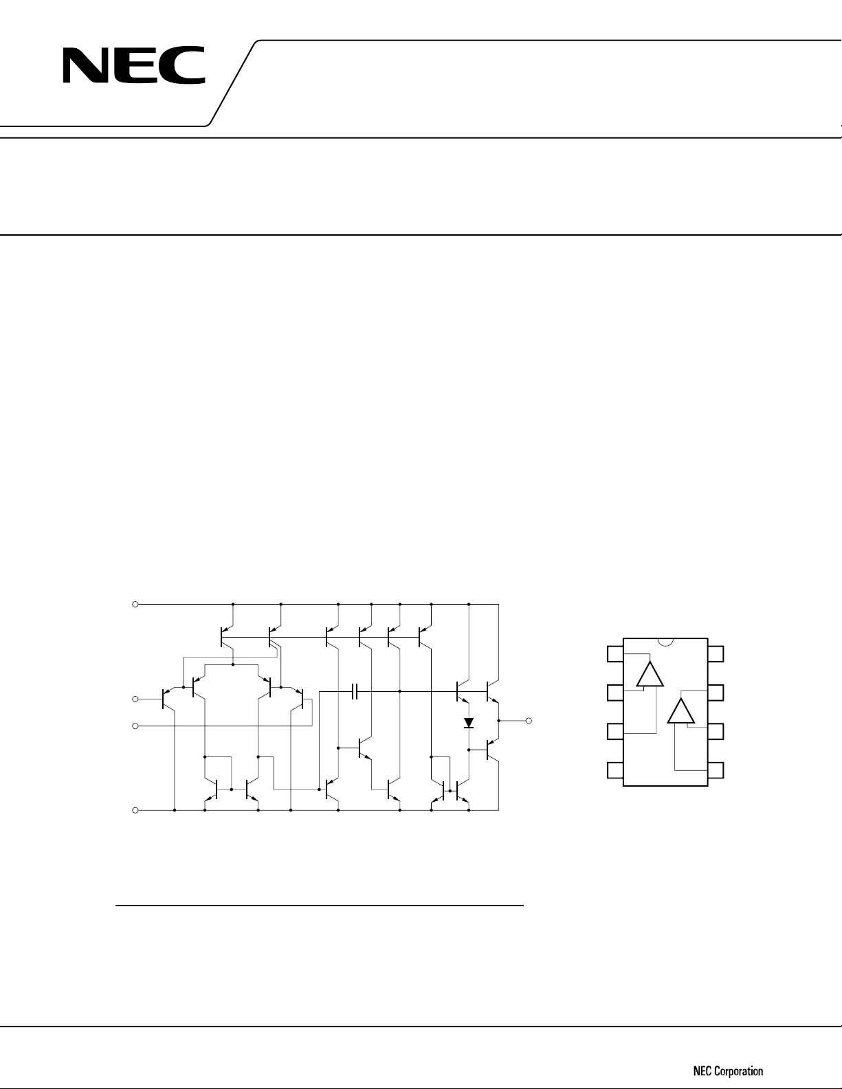
EQUIVALENT CIRCUIT (1/2 Circuit)
+
V
Q7 Q8 Q9 Q10 Q11
II
IN
–
V
Q2 Q3
Q6Q5
Q4Q1
Q14
Q15Q13
ORDERING INFORMATION
Part Number Package
µ
PC4742C 8-pin plastic DIP (300 mil)
µ
PC4742G2 8-pin plastic SOP (225 mil)
Q12
Q18
PIN CONFIGURATION
(Top View)
µ
PC4742C, 4742G2
1
OUT
1
1
+
Q19
OUT
Q20
Q17Q16
I
I1
I
N1
–
V
–
2
2
+
–
3
4
+
8
V
OUT
2
7
I
I2
6
I
N2
5
The information in this document is subject to change without notice.
Document No. G13958EJ1V0DS00 (1st edition)
Date Published December 1998 N CP(K)
Printed in Japan
©
1998
ABSOLUTE MAXIMUM RATINGS (TA = 25 °C)
Parameter Symbol Ratings Unit
–
Voltage between V+ and V
Differential Input Voltage VID ±36 V
Input Voltage
Output Voltage
Power Dissipation C Package
Output Short Circuit Duration
Operating Ambient Temperature TA –20 to +80 °C
Storage Temperature Tstg –55 to + 125 °C
Note 2
Note 3
Note 1
G2 Package
Note 6
Note 4
Note 5
Notes 1. Reverse connection of supply voltage can cause destruction.
2. The input voltage should be allowed to input without damage or destruction independent of the
magnitude of V+. Either input signal should not be allowed to go negative by more than 0.3 V. The normal
operation will establish when the both inputs are within the Common Mode Input Voltage Range of
electrical characteristics.
3. This specification is the voltage which should be allowed to supply to the output terminal from external
without damage or destructive. Even during the transition period of supply voltage, power on/off etc.,
this specification should be kept. The output voltage of normal operation will be the Output Voltage Swing
of electrical characteristics.
4. Thermal derating factor is –5.0 mW/°C when operating ambient temperature is higher than 55 °C.
5. Thermal derating factor is –4.4 mW/°C when operating ambient temperature is higher than 25 °C.
6. Pay careful attention to the total power dissipation not to exceed the absolute maximum ratings, Note
4 and Note 5.
–
V+ –V
VI V– –0.3 to V– +36 V
VO V– –0.3 to V+ +0.3 V
PT 350 mW
–0.3 to +36 V
440 mW
Indefinite sec
µ
PC4742
RECOMMENDED OPERATING CONDITIONS
Parameter Symbol MIN. TYP. MAX. Unit
Supply Voltage (Split) V
Supply Voltage (V– = GND) V
Output Current IO ±10 mA
Capacitive Load (AV = +1, Rf = 0 Ω)CL 1000 pF
±
+
±1.5 ±16 V
+3 +32 V
2
µ
PC4742
ELECTRICAL CHARACTERISTICS (TA = 25 °C, V± = ±15 V)
Parameter Symbol Conditions MIN. TYP. MAX. Unit
Input Offset Voltage VIO ±1.0 ±4.5 mV
Input Offset Current IIO ±6 ±75 nA
Input Bias Current
Large Signal Voltage Gain AV RL ≥ 2 kΩ, VO = ±10 V 25000 300000
Supply Current ICC IO = 0 A, Both Amplifiers 4.3 5.5 mA
Common Mode Rejection Ratio CMR 70 86 dB
Supply Voltage Rejection Ratio SVR 70 93 dB
Output Voltage Swing Vom RL ≥ 10 kΩ±13.7 +14 V
Output Voltage Swing Vom RL ≥ 2 kΩ±13.5 V
Common Mode lnput Voltage Range
Slew Rate (Rise) SR AV = 1, RL ≥ 2 kΩ 8.5 V/µs
Gain Band Width Product GBW fO = 100 kHz 3.5 MHz
Channel Separation f = 20 Hz to 20 kHz 120 dB
Note 7
IB 140 500 nA
–14.3
VICM V
–
V+–1.8 V
ELECTRICAL CHARACTERISTICS (TA = 25 °C, V+ = 5 V, V– = GND)
Parameter Symbol Conditions MIN. TYP. MAX. Unit
Input Offset Voltage VIO ±1.0 ±5mV
Input Offset Current IIO ±6 ±75 nA
stage.
Note 7
IB 160 500 nA
00
VICM 0V
+
IN = +1 V, V–IN = 0 V 10 30 mA
+
IN = 0 V, V–IN = +1 V 10 30 mA
+
–1.8 V
Input Bias Current
Large Signal Voltage Gain AV RL ≥ 2 kΩ 25000 300000
Supply Current ICC IO = 0 A, All Amplifiers 3.3 4.5 mA
Common Mode Rejection Ratio CMR 70 80 dB
Supply Voltage Rejection Ratio SVR 70 95 dB
Output Voltage Swing Vom RL ≥ 2 kΩ (Connect to GND) 3.7 4.0 V
Common Mode lnput Voltage Range
Output Current (SOURCE) IO SOURCE V
Output Current (SINK) IO SINK V
Slew Rate (Rise) SR 7 V/µs
Notes 7. Input bias currents flow out from IC. Because each currents are base current of PNP-transistor on input
3
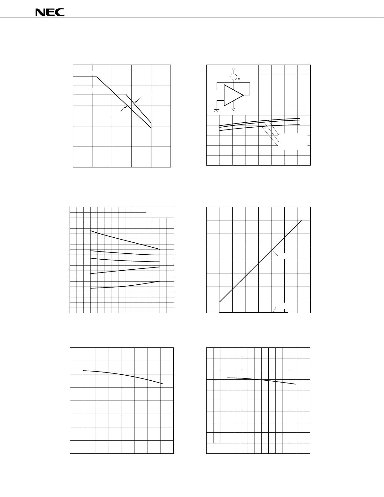
TYPICAL CHARACTERISTICS (TA = 25 °C, TYP.)
µ
PC4742
POWER DISSIPATION
500
µ
PC4742G2
400
PC4742C
µ
200 °C/W
300
227 °C/W
200
- Total Power Dissipation - mWV
T
100
P
0 20406080100
A
- Operating Ambient Temperature - °C
T
INPUT OFFSET VOLTAGE
5
V± = ±15V
4
3
2
1
0
–1
–2
- Input Offset Voltage - mV
IO
–3
–4
–5
–50 0 10050
A
- Operating Ambient Temperature - °C
T
SUPPLY CURRENT
10
+
V
A
I
CC
8
–
6
+
–
V
4
- Supply Current - mA
CC
I
2
0
±5 ±10 ±15 ±20
TA = –20 °C
T
A
= +25 °C
T
A
= +80 °C
V± - Supply Voltage - V
COMMON MODE INPUT VOLTAGE RANGE
40
30
+
V
20
ICM
10
- Common Mode Input Voltage Range - V
ICM
V
–
V
ICM
0 10203040
+
- Supply Voltage - V (V– = GND)
V
200
INPUT BIAS CURRENT
200
INPUT BIAS CURRENT
150
100
- Input Bias Current - nA
B
I
50
100
- Input Bias Current - nA
B
I
V± = ±15V
0 10203040
+
- Supply Voltage - V (V– = GND)
V
0
TA - Operating Ambient Temperature - °C
500–50 100
4

µ
PC4742
OUTPUT SINK CURRENT LIMIT
10
+
= 15 V
V
1
+
V
V+/2
0.1
- Output Voltage - V
O
V
+
–
R
The dotted line shows a
0.01
0.01 0.1 1.0 10 100
I
O SINK
characteristic of R
- Output Sink Current - mA
L
= 1 kΩ
OPEN LOOP FREQUENCY RESPONSE
120
V± = ±15 V
100
I
O SINK
L
OUTPUT SOURCE CURRENT LIMIT
5
+
= 15 V
+
- V
V
V+/2
4
+
V
∆V
I
O SOURCE
O
+
–
3
2
V
O
- Output Voltage to V
O
∆V
1
0
0.01 0.1 1.0 10 100
I
O SOURCE
- Output Source Current - mA
LARGE SIGNAL FREQUENCY RESPONSE
30
V± = ±15 V
R
L
= 2 kΩ
p-p
80
60
40
- Open Loop Voltage Gain - dB
V
20
A
0 10 100 1 k 10 k 100 k 1 M 10 M
f - Frequency - Hz
VOLTAGE FOLLOWER PULSE RESPONSE
RL = 2 kΩ
3
2
+
V
= +5 V
–
= GND
V
1
0
- Output Voltage - V
O
3
2
20
10
- Output Voltage Swing - V
om
V
0
100 1 k 10 k 100 k 1 M 10 M
f - Frequency - Hz
SLEW RATE
12
10
µ
8
6
4
SR - Slew Rate - V/ s
SR
SR
–
+
1
- Input Voltage -V/V
0
IN
V
0123
t - Time - s
µ
2
V± = ±15 V
R
L
= 2 kΩ
0
TA - Operating Ambient Temperature - °C
100500–50
5

PACKAGE DRAWINGS
8PIN PLASTIC DIP (300 mil)
85
14
µ
PC4742
A
I
P
J
H
G
C
B
F
DN
NOTES
1) Each lead centerline is located within 0.25 mm (0.01 inch) of
its true position (T.P.) at maximum material condition.
2) ltem "K" to center of leads when formed parallel.
M
K
L
M
ITEM MILLIMETERS INCHES
A 10.16 MAX. 0.400 MAX.
B 1.27 MAX. 0.050 MAX.
C 2.54 (T.P.) 0.100 (T.P.)
D 0.50±0.10 0.020
F 1.4 MIN. 0.055 MIN.
G 3.2±0.3 0.126±0.012
H 0.51 MIN. 0.020 MIN.
I 4.31 MAX. 0.170 MAX.
J 5.08 MAX. 0.200 MAX.
K 7.62 (T.P.) 0.300 (T.P.)
L 6.4 0.252
M 0.25 0.010
N 0.25 0.01
P 0.9 MIN.
R 0~15° 0~15°
+0.10
–0.05
R
+0.004
–0.005
+0.004
–0.003
0.035 MIN.
P8C-100-300B,C-1
6

8 PIN PLASTIC SOP (225 mil)
85
detail of lead end
P
µ
PC4742
1
4
A
F
G
S
B
E
D
NOTE
Each lead centerline is located within 0.12 mm of
its true position (T.P.) at maximum material condition.
C
M
M
H
I
L
K
ITEM MILLIMETERS
A
B
C
D 0.42
E
F
G
H
I
J
K 0.17
L 0.6±0.2
M
N
P3°
+0.17
5.2
−0.20
0.78 MAX.
1.27 (T.P.)
+0.08
−0.07
0.1±0.1
1.59±0.21
1.49
6.5±0.3
4.4±0.15
1.1±0.2
+0.08
−0.07
0.12
0.10
+7°
−3°
S8GM-50-225B-5
J
NS
7

µ
PC4742
RECOMMENDED SOLDERING CONDITIONS
When soldering this product, it is highly recommended to observe the conditions as shown below. If other soldering
processes are used, or if the soldering is performed under different conditions, please make sure to consult with our
sales offices.
For more details, refer to our document “Semiconductor Device Mounting Technology Manual” (C10535E).
Type of Surface Mount Device
µ
PC4742G2: 8-pin plastic SOP (225 mil)
Process Conditions Symbol
Infrared ray reflow Peak temperature: 230 °C or below (Package surface temperature), IR30-00-1
Reflow time: 30 seconds or less (at 210 °C or higher),
Maximum number of reflow processes: 1 time.
Vapor Phase Soldering Peak temperature: 215 ° C or below (Package surface temperature), VP15-00-1
Reflow time: 40 seconds or less (at 200 °C or higher),
Maximum number of reflow processes: 1 time.
Wave Soldering Solder temperature: 260 °C or below, Flow time: 10 seconds or less, WS60-00-1
Maximum number of flow processes: 1 time,
Pre-heating temperature: 120 °C or below (Package surface temperature).
Partial heating method Pin temperature: 300 °C or below, –
Heat time: 3 seconds or less (Per each side of the device).
Caution Apply only one kind of soldering condition to a device, except for “partial heating method”, or
the device will be damaged by heat stress.
Type of Through-hole Device
µ
PC4742C: 8-pin plastic DIP (300 mil)
Process Conditions
Wave soldering Solder temperature: 260 °C or below,
(only to leads) Flow time: 10 seconds or less.
Partial heating method Pin temperature: 300 °C or below,
Heat time: 3 seconds or less (per each lead).
Caution For through-hole device, the wave soldering process must be applied only to leads, and make
sure that the package body does not get jet soldered.
8

REFERENCE DOCUMENTS
QUALITY GRADES ON NEC SEMICONDUCTOR DEVICES C11531E
SEMICONDUCTOR DEVICE MOUNTING TECHNOLOGY MANUAL C10535E
NEC IC PACKAGE MANUAL (CD-ROM) C13388E
GUIDE TO QUALITY ASSUARANCE FOR SEMICONDUCTOR DEVICES MEI-1202
SEMICONDUCTORS SELECTION GUIDE X10679E
NEC SEMICONDUCTOR DEVICE RELIABILITY/QUALITY CONTROL SYSTEM IEI-1212
(STANDARD LINEAR IC)
µ
PC4742
9

[MEMO]
µ
PC4742
10

[MEMO]
µ
PC4742
11

µ
PC4742
[MEMO]
No part of this document may be copied or reproduced in any form or by any means without the prior written
consent of NEC Corporation. NEC Corporation assumes no responsibility for any errors which may appear in
this document.
NEC Corporation does not assume any liability for infringement of patents, copyrights or other intellectual property
rights of third parties by or arising from use of a device described herein or any other liability arising from use
of such device. No license, either express, implied or otherwise, is granted under any patents, copyrights or other
intellectual property rights of NEC Corporation or others.
While NEC Corporation has been making continuous effort to enhance the reliability of its semiconductor devices,
the possibility of defects cannot be eliminated entirely. To minimize risks of damage or injury to persons or
property arising from a defect in an NEC semiconductor device, customers must incorporate sufficient safety
measures in its design, such as redundancy, fire-containment, and anti-failure features.
NEC devices are classified into the following three quality grades:
"Standard", "Special", and "Specific". The Specific quality grade applies only to devices developed based on a
customer designated "quality assurance program" for a specific application. The recommended applications of
a device depend on its quality grade, as indicated below. Customers must check the quality grade of each device
before using it in a particular application.
Standard: Computers, office equipment, communications equipment, test and measurement equipment,
audio and visual equipment, home electronic appliances, machine tools, personal electronic
equipment and industrial robots
Special: Transportation equipment (automobiles, trains, ships, etc.), traffic control systems, anti-disaster
systems, anti-crime systems, safety equipment and medical equipment (not specifically designed
for life support)
Specific: Aircrafts, aerospace equipment, submersible repeaters, nuclear reactor control systems, life
support systems or medical equipment for life support, etc.
The quality grade of NEC devices is "Standard" unless otherwise specified in NEC's Data Sheets or Data Books.
If customers intend to use NEC devices for applications other than those specified for Standard quality grade,
they should contact an NEC sales representative in advance.
Anti-radioactive design is not implemented in this product.
M4 96.5
 Loading...