

Page 1
DATA SHEET
BIPOLAR ANALOG INTEGRATED CIRCUIT
µµµµ
PC4741
HIGH PERFORMANCE QUAD OPERATIONAL AMPLIFIER
DESCRIPTION
The µPC4741 consists of four independent frequency compensated operational amplifiers featuring higher speed,
broader band than general purpose type as 741. The
such as active filters or pulse amplifiers.
FEATURES
• Internal frequency compensation
• Low noise
• Output short circuit protection
PC4741 is most appropriate for AC signal amplifier applications
µ
ORDERING INFORMATION
Part Number Package
PC4741C
µ
PC4741C(5)
µ
PC4741G2
µ
PC4741G2(5)
µ
14-pin plastic DIP (7.62 mm (300))
14-pin plastic DIP (7.62 mm (300))
14-pin plastic SOP (5.72 mm (225))
14-pin plastic SOP (5.72 mm (225))
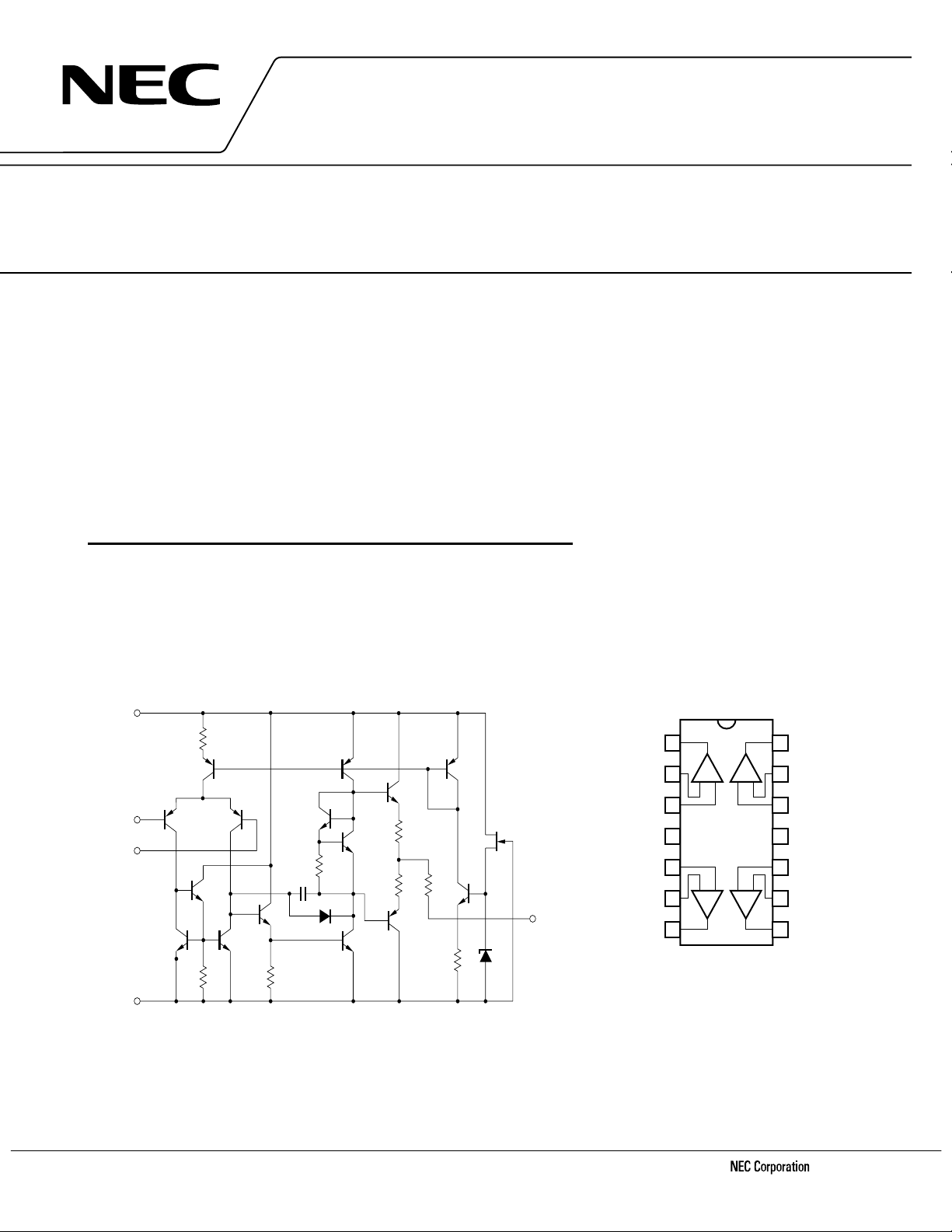
EQUIVALENT CIRCUIT (1/4 Circuit)
+
V
R
1
Q
5
Q
1
Q
I
I
I
N
Q
3
–
V
2
Q
6
Q
4
R
2
Q
8
R
C
1
Q
7
R
3
PIN CONFIGURATION (Top View)
µ
PC4741C, 4741G2
1
OUT
OUT
1
14
2
I
I1
−+
3
I
N1
+
4
V
5
I
N2
−+
6
I
I2
2
23
7
Q
9
Q
14
Q
12
Q
R
Q
10
4
D
1
Q
11
5
R
7
R
6
Q
15
Q
13
R
8
16
OUT
D
2
14
13
−+
12
11
10
−+
OUT
4
I
I4
I
N4
−
V
I
N3
I
I3
9
OUT
3
8
The information in this document is subject to change without notice. Before using this document, please
confirm that this is the latest version.
Not all devices/types available in every country. Please check with local NEC representative for
availability and additional information.
Document No. G16051EJ3V0DS00 (3rd edition)
(Previous No. IC-1197)
Date Published February 2002 NS CP(K)
Printed in Japan
The mark ★ shows major revised points.
©
1987
Page 2
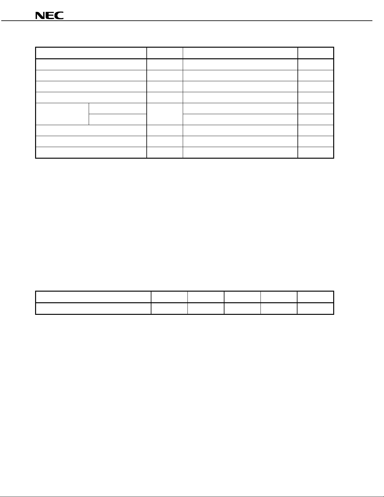
ABSOLUTE MAXIMUM RATINGS (TA = 25°C)
Parameter Symbol Ratings Unit
−
Voltage between V+ and V
Note1
V+ − V
µµµµ
PC4741
−
−0.3 to +40 V
Differential Input Vol t age V
Input Voltage
Output Voltage
Output Short Circuit Durati on
Note2
Note3
C Package
G2 Package
Note6
Note4
Note5
Operating Ambient Temperature T
Storage Temperature T
ID
I
V
O
V
T
P
±30 V
−
V
−0.3 to V
−
V
−0.3 to V
+
+0.3
+
+0.3
570 mWPower Dissipation
550 mW
10 sec
A
stg
−20 to +80 °C
−55 to +125 °C
Notes 1. Reverse connection of supply voltage can cause destruction.
The input voltage should be allowed to input without damage or destruction. Even during the transition
2.
period of supply voltage, power on/off etc., this specification should be kept. The normal operation will
establish when the both inputs are within the Common Mode Input Voltage Range of electrical
characteristics.
3. This specification is the voltage which should be allowed to supply to the output terminal from external
without damage or destructive. Even during the transition period of supply voltage, power on/off etc., this
specification should be kept. The output voltage of normal operation will be the Output Voltage Swing of
electrical characteristics.
4. Thermal derating factor is –7.6 mW/°C when ambient temperature is higher than 50°C.
5. Thermal derating factor is –5.5 mW/°C when ambient temperature is higher than 25°C.
Pay careful attention to the total power dissipation not to exceed the absolute maximum ratings, Note 4 and
6.
Note 5.
V
V
RECOMMENDED OPERATING CONDITIONS
Parameter Symbol MIN. TYP. MAX. Unit
Supply Voltage V
2
Data Sheet G16051EJ3V0DS
±
±4 ±16 V
Page 3
PC4741C, 4741G2
µµµµ
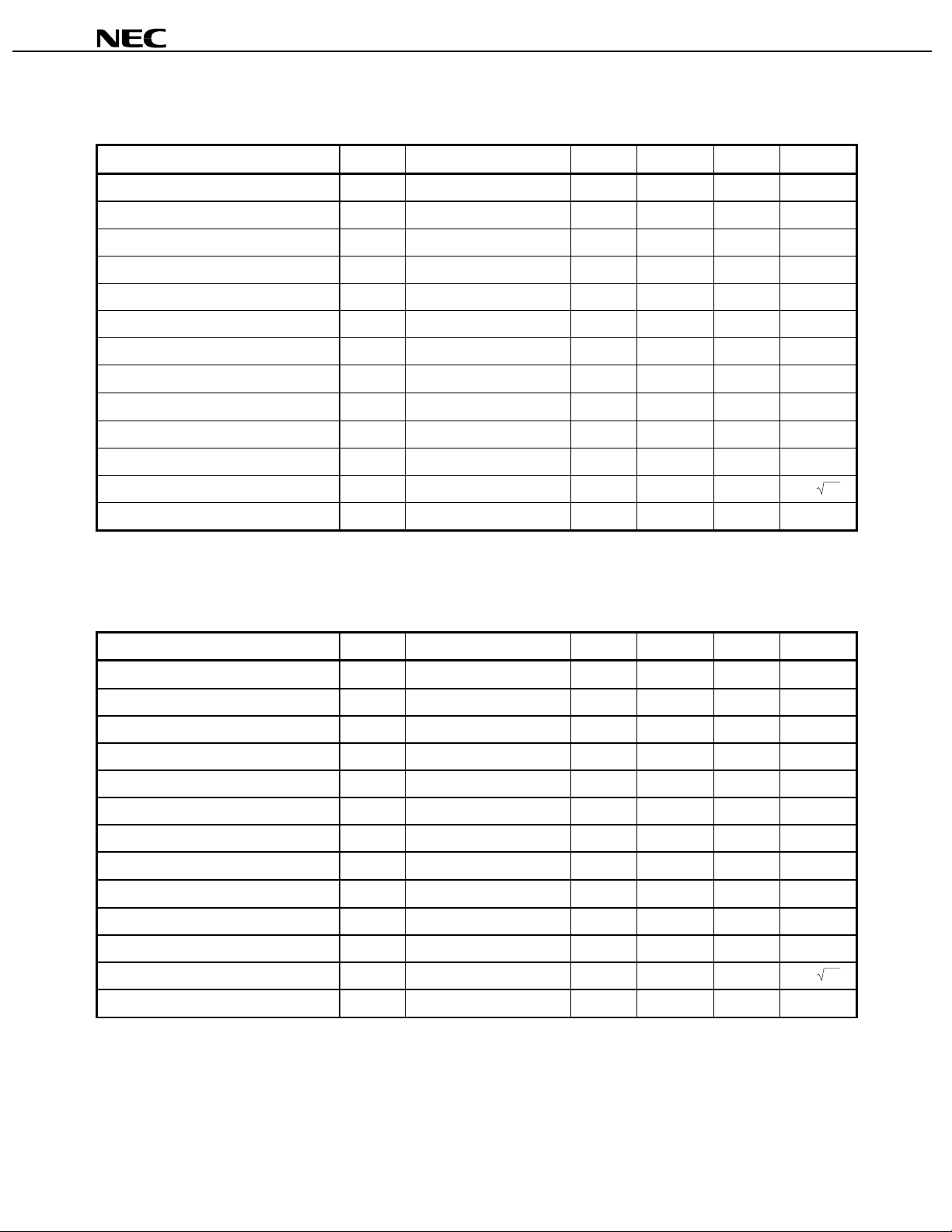
ELECTRICAL CHARACTERISTICS (T
Parameter Symbol Conditions MIN. TYP. MAX. Unit
= 25°C, V
A
±±±±
= ±±±±15 V)
µµµµ
PC4741
Input Offset Voltage V
Input Offset Current
Input Bias Current
Note
Note
Large Signal Voltage Gain A
IO
RS ≤ 100 Ω±1.0 ±5.0 mV
IO
I
B
I
V
RL ≥ 2 kΩ , VO = ±10 V 25,000 50,000
±30 ±50 nA
70 300 nA
Power Consumption Pd IO = 0 A, All Amplif i ers 150 210 mW
Common Mode Rejection Rati o CMR 80 100 dB
Supply Voltage Rejection Rat i o SVR 50 100
Maximum Output Voltage V
Maximum Output Voltage V
Common Mode Input Voltage Range V
om
RL ≥ 10 kΩ±12 ±13.7 V
om
RL ≥ 2 kΩ±10 ±12.5 V
ICM
±12 ±14 V
Slew Rate SR AV = 1 1.6 V/ µs
Input Equivalent Noise Vol t age Density e
n
f = 1 kHz 9 nV/ Hz
Channel Separation f = 10 kHz 108 dB
Input bias currents flow out from IC. Because each currents are base current of PNP-transistor on input stage.
Note
PC4741C (5), 4741G2 (5)
µµµµ
ELECTRICAL CHARACTERISTICS (T
= 25°C, V
A
±±±±
= ±±±±15 V)
µ
V/ V
Parameter Symbol Conditions MIN. TYP. MAX. Unit
Input Offset Voltage V
Input Offset Current
Input Bias Current
Note
Note
Large Signal Voltage Gain A
IO
RS ≤ 100 Ω±1.0 ±2.0 mV
IO
I
B
I
V
RL ≥ 2 kΩ , VO = ±10 V 28,000 50,000
±30 ±50 nA
100 nA
Power Consumption Pd IO = 0 A, All Amplif i ers 150 210 mW
Common Mode Rejection Rati o CMR 85 90 dB
Supply Voltage Rejection Rat i o SVR 50
Maximum Output Voltage V
Maximum Output Voltage V
Common Mode Input Voltage Range V
om
RL ≥ 10 kΩ±12.5 ±13.7 V
om
RL ≥ 2 kΩ±11 ±12.5 V
ICM
±13 ±14 V
µ
V/ V
Slew Rate SR AV = 1 1.6 V/ µs
Input Equivalent Noise Vol t age Density e
n
f = 1 kHz 9 nV/ Hz
Channel Separation f = 10 kHz 108 dB
Note Input bias currents flow out from IC. Because each currents are base current of PNP-transistor on input stage.
Data Sheet G16051EJ3V0DS
3
Page 4
MEASUREMENT CIRCUIT
Fig.1 Channel Separation Measurement Circuit
50 kΩ
50 Ω
−
+
V
O2
Channel Separation
= 20 log
1
1000
µµµµ
PC4741
V
O2
V
O1
10 kΩ
10 kΩ
−
+
V
O1
4
Data Sheet G16051EJ3V0DS
Page 5
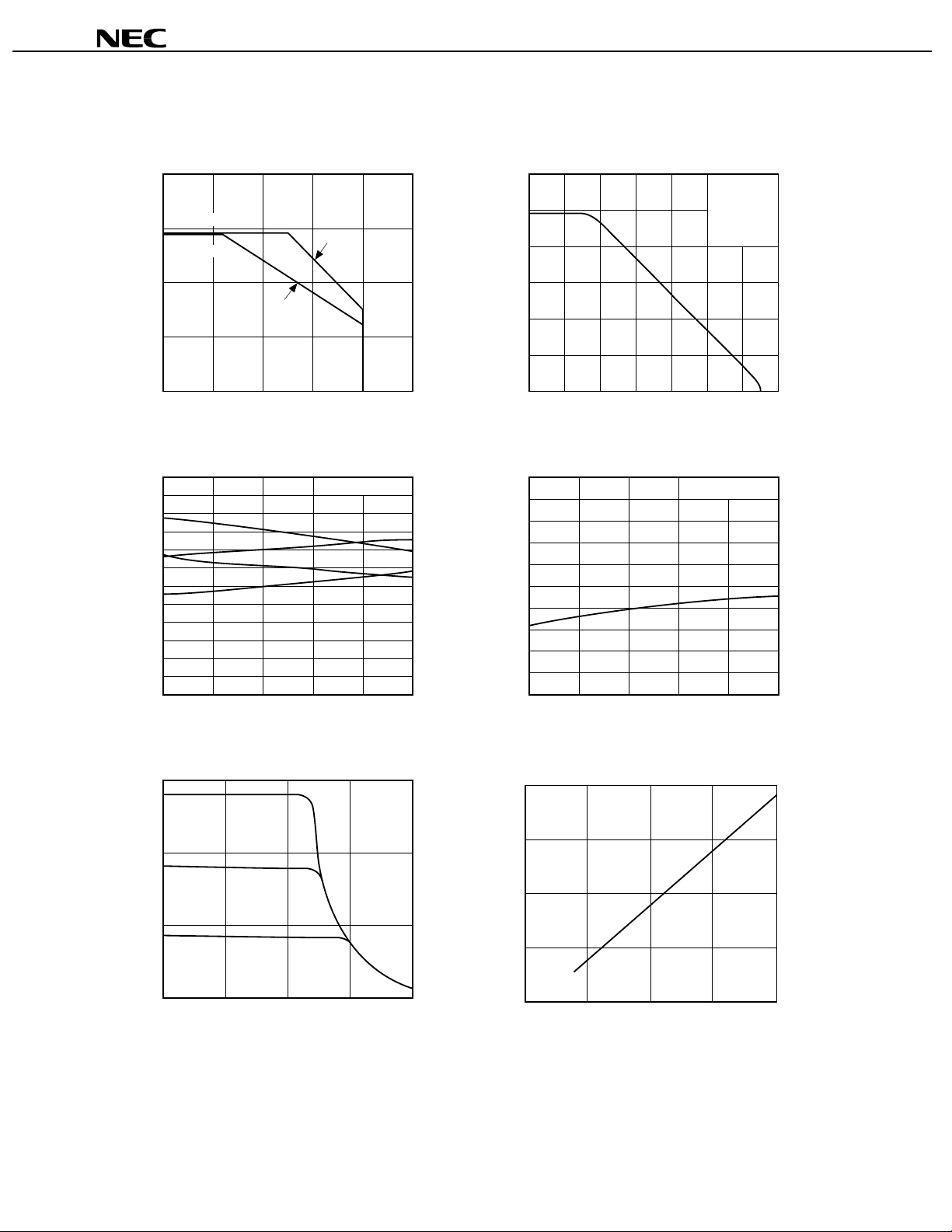
TYPICAL PERFORMANCE CHARACTERISTICS (TA = 25°C, TYP.)
TA - Operating Ambient Temperature - ˚C
POWER DISSIPATION
P
T
- Total Power Dissipation - mW
800
600
400
200
0
20
40 60 80 100
PC4741G2
µ
PC4741C
µ
132˚C/W
182˚C/W
OPEN LOOP FREQUENCY RESPONSE
120
100
80
60
40
- Open Loop Voltage Gain - dB
20
V
A
0
1 100 10 k 1 M1 k10 100 k 10 M
f - Frequency - Hz
V± = ±15 V
R
L
= 2 k
Ω
CL = 50 pF
µµµµ
PC4741
3
2.5
2
1.5
1
0.5
0
−0.5
−1
- Input Offset Voltage - mV
−1.5
IO
V
−2
−2.5
−3
−20
TA - Operating Ambient Temperature -
LARGE SIGNAL FREQUENCY RESPONSE
30
p-p
20
INPUT OFFSET VOLTAGE
±
V= ±15 V
020406080
˚C
±
V= ±15 V
±
V= ±10 V
100
95
90
85
80
75
70
65
- Input Bias Current - nA
B
I
60
55
50
−20
COMMON MODE INPUT VOLTAGE RANGE
40
30
20
INPUT BIAS CURRENT
±
V= ±15 V
020406080
TA - Operating Ambient Temperature -
˚C
10
- Output Voltage Swing - V
om
V
0
100 1 k 10 k 100 k 1 M
±
V= ±5 V
f - Frequency - Hz
10
- Common Mode Input Voltage Range - V
ICM
V
0
Data Sheet G16051EJ3V0DS
±
±
V - Supply Voltage - V
10
±
20
5
Page 6
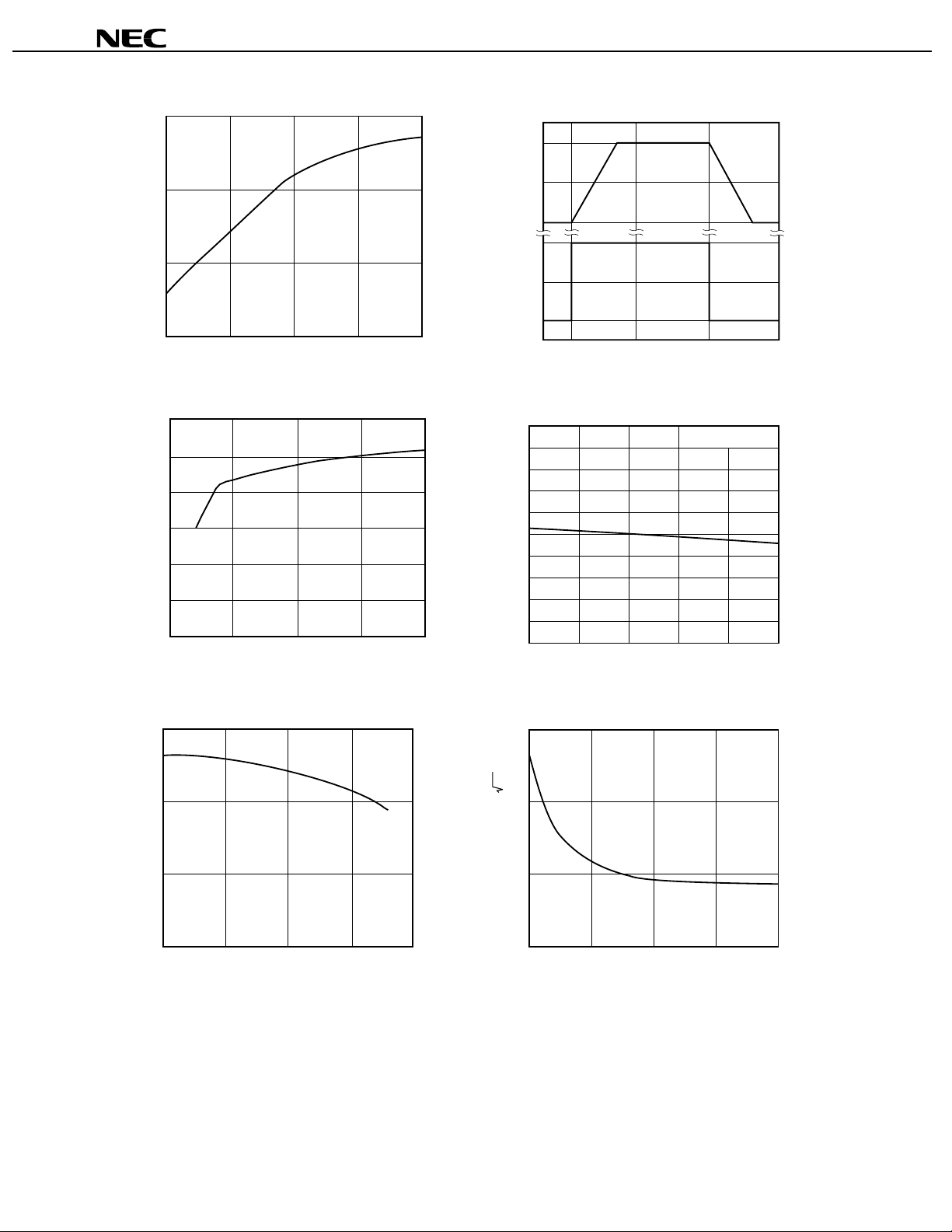
µµµµ
f - Frequency - Hz
INPUT EQUIVALENT NOISE VOLTAGE DENSITY
e
n
- Input Equivalent Noise
Voltage Density - nV/ Hz
0
10
20
30
100 1 k 10 k 100 k10
PC4741
OUTPUT VOLTAGE SWING
30
p-p
20
10
- Output Voltage Swing - V
om
V
0
100 300 1 k 3 k 10 k
R
L
- Load Resistance -
Ω
SUPPLY CURRENT
6
5
4
3
2
- Supply Current - mA
CC
I
1
±
0
±
5
V - Supply Voltage - V
±
±
10
15
VOLTAGE FOLLOWER PULSE RESPONSE
V= ±15 V
−5
R
CL= 50 pF
±
L
= 2 kΩ
0
- Output Voltage - V
O
V
−5
5
0
−5
- Input Voltage - V
I
V
10
9
010 2030
t - Time - s
µ
SUPPLY CURRENT
±
V= ±15 V
8
7
6
5
4
- Supply Current - mA
3
CC
I
2
1
±
20
0
−20
020406080
TA - Operating Ambient Temperature -
˚C
150
100
50
Channel Separation - dB
0
10 100 1 k 10 k 100 k
6
CHANNEL SEPARATION
f - Frequency - Hz
Data Sheet G16051EJ3V0DS
Page 7
★
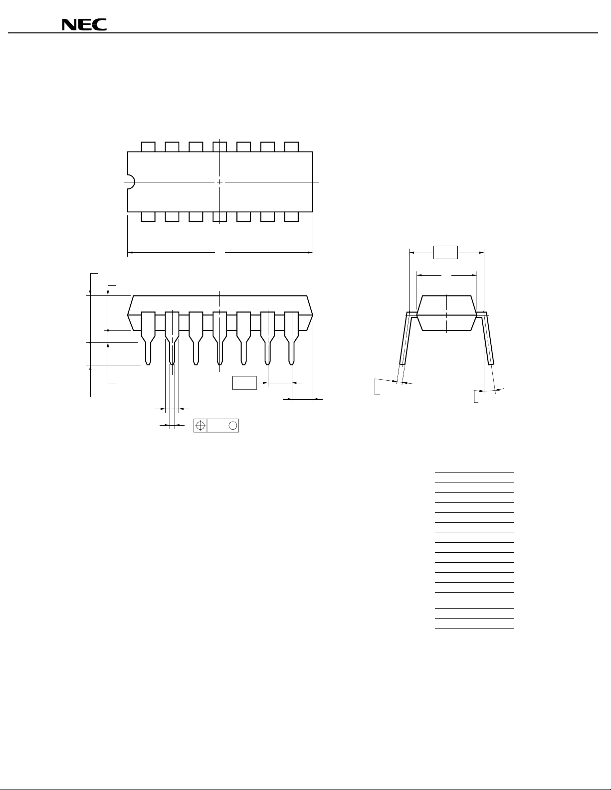
PACKAGE DRAWINGS (Unit: mm)
14-PIN PLASTIC DIP (7.62 mm (300))
14 8
17
µµµµ
PC4741
A
J
I
H
C
G
F
DN
NOTES
1. Each lead centerline is located within 0.25 mm of
its true position (T.P.) at maximum material condition.
2. ltem "K" to center of leads when formed parallel.
M
K
L
B
M
ITEM MILLIMETERS
A
B
C
D
F
G
H 0.51 MIN.
I
J
K 7.62 (T.P.)
L 6.4±0.2
M 0.25
N 0.25
R
R
19.22±0.2
2.14 MAX.
2.54 (T.P.)
0.50±0.10
1.32±0.12
3.6±0.3
3.55
4.3±0.2
+0.10
−0.05
0~15°
P14C-100-300B1-3
Data Sheet G16051EJ3V0DS
7
Page 8
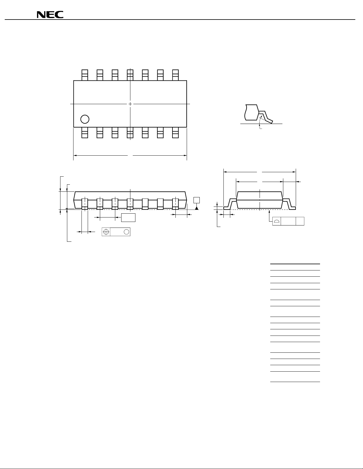
14-PIN PLASTIC SOP (5.72 mm (225))
14 8
17
A
detail of lead end
P
µµµµ
PC4741
F
G
C
D
M
M
B
E
NOTE
Each lead centerline is located within 0.1 mm of
its true position (T.P.) at maximum material condition.
H
I
J
S
L
NS
K
ITEM
MILLIMETERS
A 10.2±0.26
B
1.42 MAX.
C
1.27 (T.P.)
D
E
F
G
H
I
J
K
L
M
N
P
S14GM-50-225B, C-6
+0.08
0.42
−0.07
0.1±0.1
+0.21
1.59
−0.2
1.49
6.5±0.2
4.4±0.1
1.1±0.16
+0.08
0.17
−0.07
0.6±0.2
0.1
0.10
+7°
3°
−3°
8
Data Sheet G16051EJ3V0DS
Page 9

µµµµ
PC4741
★
RECOMMENDED SOLDERING CONDITIONS
W hen soldering this product, it is highly recommended to observe the conditions as shown below. If other soldering
processes are used, or if the soldering is performed under different conditions, please make sure to consult with our sales
offices.
For more details, refer to below our document "SEMICONDUCTOR DEVICE MOUNTING TECHNOLOGY
MANUAL"(C10535E).
Type of Surface Mount Device
µµµµ
PC4741G2, 4741G2(5): 14-pin plastic SOP (5.72 mm (225))
Process Conditions Symbol
Infrared Ray Reflow P eak temperature: 235°C or below (Pack age surface temperature),
Reflow time: 30 seconds or less (at 210°C or higher),
Maximum number of reflow process es: 3 time.
Vapor Phase Soldering Peak temperature: 215°C or below (Package surface temperature),
Reflow time: 40 seconds or less (at 200°C or higher),
Maximum number of reflow process es: 3 time.
Wave Soldering Solder temperature: 260°C or below, Flow time: 10 seconds or less,
Maximum number of flow process es: 1 time,
Pre-heating temperature: 120°C or bel ow (Pac kage surface temperature).
Partial Heating Method Pin temperature: 300°C or below,
Heat time: 3 seconds or less (Per each side of the device).
IR35-00-3
VP15-00-3
WS60-00-1
–
Caution Apply only one kind of soldering condition to a device, except for "partial heating method", or the
device will be damaged by heat stress.
Type of Through-hole Device
µµµµ
PC4741C, 4741C(5): 14-pin plastic DIP (7.62 mm (300))
Process Conditions
Wave Soldering
(only to leads)
Solder temperature: 260°C or below,
Flow time: 10 seconds or less .
Partial Heating Method Pin temperature: 300° C or bel ow,
Heat time: 3 seconds or less (per each lead).
Caution For through-hole device, the wave soldering process must be applied only to leads, and make sure that
the package body does not get jet soldered.
Data Sheet G16051EJ3V0DS
9
Page 10

[MEMO]
µµµµ
PC4741
10
Data Sheet G16051EJ3V0DS
Page 11

[MEMO]
µµµµ
PC4741
Data Sheet G16051EJ3V0DS
11
Page 12

µµµµ
PC4741
•
The information in this document is current as of February, 2002. The information is subject to
change without notice. For actual design-in, refer to the latest publications of NEC's data sheets or
data books, etc., for the most up-to-date specifications of NEC semiconductor products. Not all
products and/or types are available in every country. Please check with an NEC sales representative
for availability and additional information.
•
No part of this document may be copied or reproduced in any form or by any means without prior
written consent of NEC. NEC assumes no responsibility for any errors that may appear in this document.
•
NEC does not assume any liability for infringement of patents, copyrights or other intellectual property rights of
third parties by or arising from the use of NEC semiconductor products listed in this document or any other
liability arising from the use of such products. No license, express, implied or otherwise, is granted under any
patents, copyrights or other intellectual property rights of NEC or others.
•
Descriptions of circuits, software and other related information in this document are provided for illustrative
purposes in semiconductor product operation and application examples. The incorporation of these
circuits, software and information in the design of customer's equipment shall be done under the full
responsibility of customer. NEC assumes no responsibility for any losses incurred by customers or third
parties arising from the use of these circuits, software and information.
•
While NEC endeavours to enhance the quality, reliability and safety of NEC semiconductor products, customers
agree and acknowledge that the possibility of defects thereof cannot be eliminated entirely. To minimize
risks of damage to property or injury (including death) to persons arising from defects in NEC
semiconductor products, customers must incorporate sufficient safety measures in their design, such as
redundancy, fire-containment, and anti-failure features.
•
NEC semiconductor products are classified into the following three quality grades:
"Standard", "Special" and "Specific". The "Specific" quality grade applies only to semiconductor products
developed based on a customer-designated "quality assurance program" for a specific application. The
recommended applications of a semiconductor product depend on its quality grade, as indicated below.
Customers must check the quality grade of each semiconductor product before using it in a particular
application.
"Standard": Computers, office equipment, communications equipment, test and measurement equipment, audio
and visual equipment, home electronic appliances, machine tools, personal electronic equipment
and industrial robots
"Special": Transportation equipment (automobiles, trains, ships, etc.), traffic control systems, anti-disaster
systems, anti-crime systems, safety equipment and medical equipment (not specifically designed
for life support)
"Specific": Aircraft, aerospace equipment, submersible repeaters, nuclear reactor control systems, life
support systems and medical equipment for life support, etc.
The quality grade of NEC semiconductor products is "Standard" unless otherwise expressly specified in NEC's
data sheets or data books, etc. If customers wish to use NEC semiconductor products in applications not
intended by NEC, they must contact an NEC sales representative in advance to determine NEC's willingness
to support a given application.
(Note)
(1) "NEC" as used in this statement means NEC Corporation and also includes its majority-owned subsidiaries.
(2) "NEC semiconductor products" means any semiconductor product developed or manufactured by or for
NEC (as defined above).
M8E 00. 4
 Loading...