

NEC NMV 1700V Service Manual

Service Manual
17-inch LCD Monitor
NMV 1700V (U170ATA)

NMV 1700V
Table of Contents
1. Audio circuit ----------------------------------------------------------------------------------------------------------------------------1
1.1 Audio input ------------------------------------------------------------------------------------------------------------------------- 1
1.2 Audio output -----------------------------------------------------------------------------------------------------------------------1
2. Power supply----------------------------------------------------------------------------------------------------------------------------1
3. Video input circuit --------------------------------------------------------------------------------------------------------------------- 1
4. Definition converter LSI peripheral circuit -------------------------------------------------------------------------------------1
5. System reset, LED control circuit ------------------------------------------------------------------------------------------------- 1
6. E2PROM for PNP ----------------------------------------------------------------------------------------------------------------------1
7. E2PR OM---------------------------------------------------------------------------------------------------------------------------------- 2
8. CPU circuit ------------------------------------------------------------------------------------------------------------------------------ 2
8.1 Dection of POWER switch status --------------------------------------------------------------------------------------------2
8.2 Display mode identification---------------------------------------------------------------------------------------------------- 2
8.3 User control ------------------------------------------------------------------------------------------------------------------------ 4
8.4 Control of identification converter LSI (IC 14)---------------------------------------------------------------------------5
8.5 I2C bus control---------------------------------------------------------------------------------------------------------------------5
8.6 Po wer ON sequence -------------------------------------------------------------------------------------------------------------- 6
8.7 Po wer OFF sequence ------------------------------------------------------------------------------------------------------------ 7
8.8 List of CPU assignments--------------------------------------------------------------------------------------------------------8
Circuit Description Index

N MV 170 0V
1. Audio circuit (C ircuit diagrams Main PWB 1/1 JACK PWB 1/1)
1.1 Audio input
The audio signal input recei ved from the audio input terminal (JK011) is applied to the pre-amplifier I006 of
2 (L-CH) and 29 (R-CH) through the low-pass filter consisting of R047, R049, R048, R050, C062 and C063.
In this pre-amplifier, contr ols of Volume, Balance, Bass, and Treble are conducted. The audio signal controlled
at the pre-amplifier is entered in and amplified at the AMP I007 of 9 (L-CH) and 1 (R-CH). Since then, the signal
is to the output jack.
1.2 Audio output
The audio signal is output from the output terminal (P012) of the jack to the speaker system.
2. Power supply (Circuit daigrams MAIN PWB 8/10, 9/10, 10/10)
1. I322:DC-DC converter
A 5V power supply for LCD modul e, CPU, and logic is generated from the 19V source.
2. I323:3-terminal regulator
A 3.3V power supply for Scaler IC I315, LVDS IC I319, I320 is generated from the 5V source.
3. I330:3-terminal regulator
A 3.3V po wer supply for SDRAM IC I316, I317, I318 is generated from the 5V source.
4. I324:3-terminal regulator
A 2.5V po wer supply for Scaler IC I315 is generated from the 5V source.
Q307, I321 ON/OFF control for LCD Module
ON/OFF co ntrol is performed for power ON/OFF and also for the power saving sequence.
3. Video input circuit (Circuit diagram MAIN PWB 4/10)
The analog video signal input entered from P304, the AC-coupled video signal is used to clamp the black level at
0V).
4. Definition converter LSI peripheral circuit (Circuit diagram MAIN PWB)
I315 gm5020 is the definition converter LSI.
The analog R, G, B signal input entered from the video input circuit is converted into the digital data of video
signal through the incorporated A/D converter. Based on this conversion, this device performs interpolation
during pi xel extension. The source voltage for this device is 3.3V, 2.5V and the system clock frequency is
24MHz. The withstand voltage level for the input signal voltage if I315 is 3.3V and 5V.
5. System reset, LED control circuit (Circuit diagram MAIN PWB 3/10)
5.1 System reset
System reset is performed by detecting the rising and falling of the 5V source voltage at I301.
5.2 LED control circuit
Green / amb er is lit with the control signal of the LED GREEN and LED AMBER signal pin 15, 12 from I306
(Circuit diagram MAIN PWB 2/8).
6. E2PROM for PnP (Circuit diagram MAIN PWB 4/10)
Page 1Circuit Description

NMV 1700V
7. E2PROM (Circuit diagram MAIN PWB 3/10)
Data tra nsfer between I305 (AT24 C16) and CPU (Circuit diagram MAIN PWB 2/8 (I302) is effected through
the IIC bus SCL (pin 15) and SDA (pin 16) of I302. The data to be transferred to each device are stored in I305.
l I315 control data.
l OSD related setting data.
l Other control data for service menu.
8. CPU circuit (Circuit diagram MAIN PWB 3/10)
I302 (87C51RD2) functions as the CPU.
The source voltage for the device is 5.0V and the system clock frequency is 24MHz.
8.1 Detection of POWER switch status
The CPU identifies the ON status of the two power supplies. The identification is made when the power supply
is turned off. For example, if the power supply is turned off w ith the POWER switch, the POWER switch must be
turned on when activating the power supply again. If t he power supply is turned off by pulling out the power
cord , then this power supply can be turned on by connecting the power cord, without pressing the POWER
switch.
8.2 Display mode identification
8.2.1 Functions
(1) Display mode identification
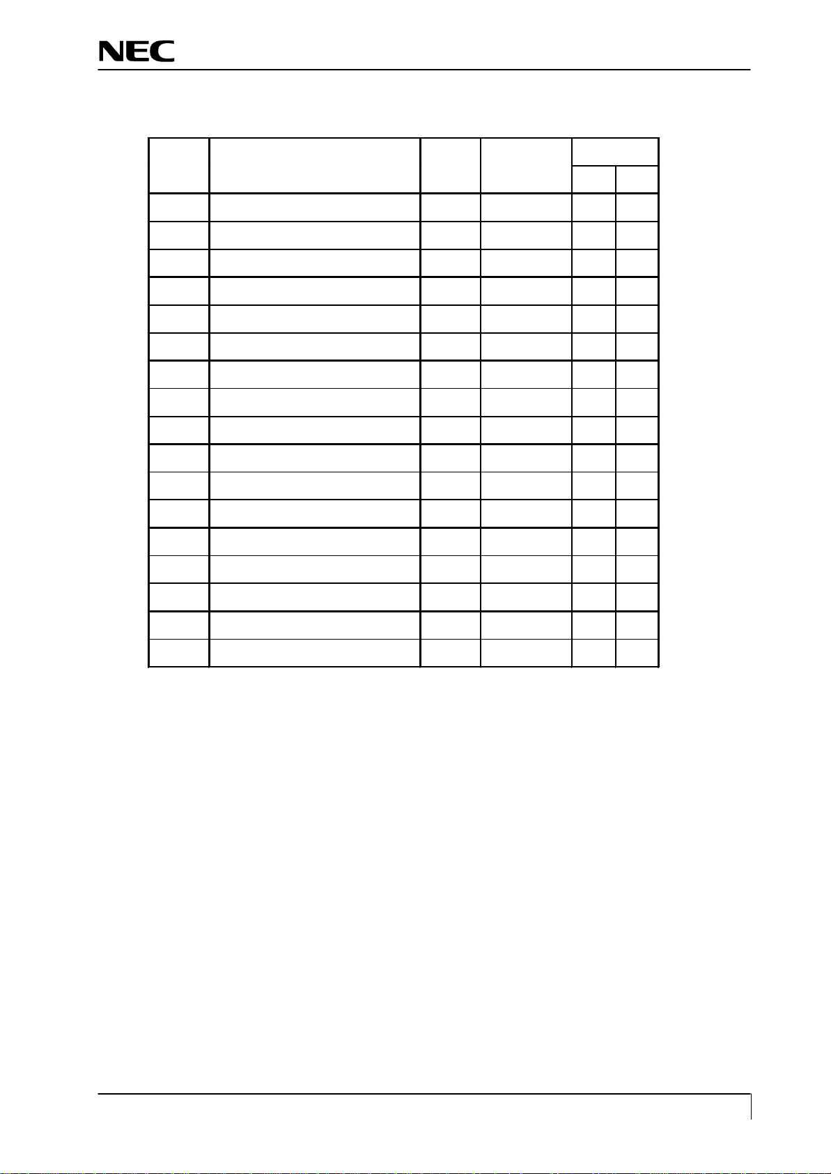
l The display mode of input signal is identified based on Table 1.
l When the mode has been identified through the measurement of horizontal and vertical frequencies, the total
number of lines is determined with a formula of “ Horizontal frequency / Vertical frequency = Total number
of li nes. “Final identification can be made by examining the coincidence of the obtained figure with the
number of lines fo r the mode identified from the frequency. The boundary number of lines in each mode is
shown in Table 2.
l When the detected frequency if the sync signal has changed, the total number of lines should be counted even
through it is rge identified frequency in the same mode.
(2) Power save mode.
This power save mode is assumed when the frequency of the horizontal / vertical signal is as specified below.
l Vertical frequen cy : 50 ~ 86 Hz
l Horizontal frequency : 24 ~ 92 KHz
l VTOTAL : 1200 or more.
(3) Power save mode.
The power save mode is assumed when the horizontal / vertical signals are as specified below.
l If there is no horizontal sync signal input.
l If there is no vertical sync signal input.
l If the horizontal sync signal is outside the measuring range of gm5020.
P ag e 2 Circ uit D e script ion
l If the vertical sync signal is outside the measuring range of gm5020.
Mode
H-freq
(KHz)
Band Width
31.47
31.47
37.86
35.16
37.88
46.88
48.08
49.72
48.36
56.48
60.02
NMV 1700V
Resolution
(MHz)
1. VGA 720 x 400 70Hz
2. VGA 640 x 480 60Hz
3. MAC 640 x 480 66Hz 35 32.24 - -
4. VESA 640 X 480 72Hz
5. VESA 640 X 480 75Hz 37.5 31.5 - -
6. VESA 800 x 600 56Hz
7. VESA 800 x 600 60Hz
8. VESA 800 x 600 75Hz
9. VESA 800 x 600 72Hz
10. MAC 832 x 624 75Hz
11. VESA 1024 x 768 60Hz
12. VESA 1024 x 768 70Hz
13. VESA 1024 x 768 75Hz
28.322 - +
25.175 - -
31.5 - -
36 + +
40 + +
49.5 + +
50 + +
57.283 - 65 - 75 - -
78.75 + +
Polarity
H V
14. VESA 1280 x 1024 60Hz 64 108 + +
15. VESA 1280 x 1024 75Hz 80 135 + +
16. VESA 1152 x 864 75Hz 67.5 108 + +
17. VESA 1280 x 960 60Hz 60 108 + +
Page 3Circuit Description
Table 1
I/O
Signal name
I315, M1
EXIT/ENTER switch input
I315, L1
I315, G18
I315, G19
I302, 15
Table 2 the number of the lines, Vsync distinction
Indication resolution The number of the
distinction lines
640 x 480 487 < LINE < 607 fV < 63 Hz 2
800 x 600 607 < LINE < 777 fV < 58 Hz 6
832 x 624 640 < LINE - 10
1024 x 768 768 < LINE < 870 fV < 63 Hz 11
1152 x 864 870 < LINE < 1031 16
1280 x 960 960 < LINE < 1027 17
1280 x 1024 1027 < LINE 14,15
NMV 1700V
Distinction Vsync The fixed mode
63 Hz < fV < 68 Hz 3
68 Hz < fV < 74 Hz 4
74 Hz < fV < 78 Hz 5
58 Hz < fV < 63 Hz 7
63 Hz < fV < 73 Hz 9
73 Hz < fV < 78 Hz 8
68 Hz < fV < 73 Hz 12
73 Hz < fV < 78 Hz 13
9.3 User Control
Port Pin No.
GPI04
GPI05
GPI06
GPI07
GPI0
9.3.2 Functions
Control is effected for the push-switches to be used when the user changes the parameters, in order to modify the
respective setting values. Whether the switch has been p ressed is identified with the switch input level that is
turned “L”.
Each switch input port is pulled up at outside of ASIC
Each parameter is stored in the EEPROM, the contents of which are upda ted as required.
.
1 MENU
1 DOWN switch input ( ) key
1 - switch input ( ) key
1 + switch input ( ) key
1 POWER soft power switch input ( power ) key
Function Remarks
ENTER/Withdraw
from OSD
Page 4 Circuit Description
8 . 4 C ont rol of d efinitio n conver t er LSI I315
Pin No.
Signal name
R1, R2
8.4.1 Ports related to control
NMV 1700V
I/O
R3 I IRQ gmZan1 interrupt signal
P1 O HCLK gmZan1 serial clock
P3, P4,
I/O HDATA gmZan1 serial data
P2 O HFS gmZan1 serial select
9. 3. 1 Related ports of I315 and pin of I302
8. 4. 2 F un ct i on s
Maj or f unction of I 315 are as f ollows:
(1) Ex pansion of t he di splay s creen.
(2) Timing cont rol for various si gnal t ypes.
Port Pin No. I/O Signal name Function
P3.5 17 I IICCLK IIC bus clock
P3.4 16 I/O IICDATA IIC bus data
(3 ) Po wer -su pply se que nce (LC D p anel ).
8 . 5 I2C bus c ontrol
8. 5.1 Related port s of I302
8. 5. 2 I2C - cont rol led f u n c t i o n s
Function
Page 5Circuit Description
The following functional controls are effected by I2C.
POWER
(1) Control o f EEPROM I305f for parameter setting.
(2) Control of audio preamplifier.
LED
LVCC
(Audio_EN)
Panel_VCC
PCLK/DATA
NMV 1700V
Backlight_EN
Page 6 Circuit Description
NMV 1700V
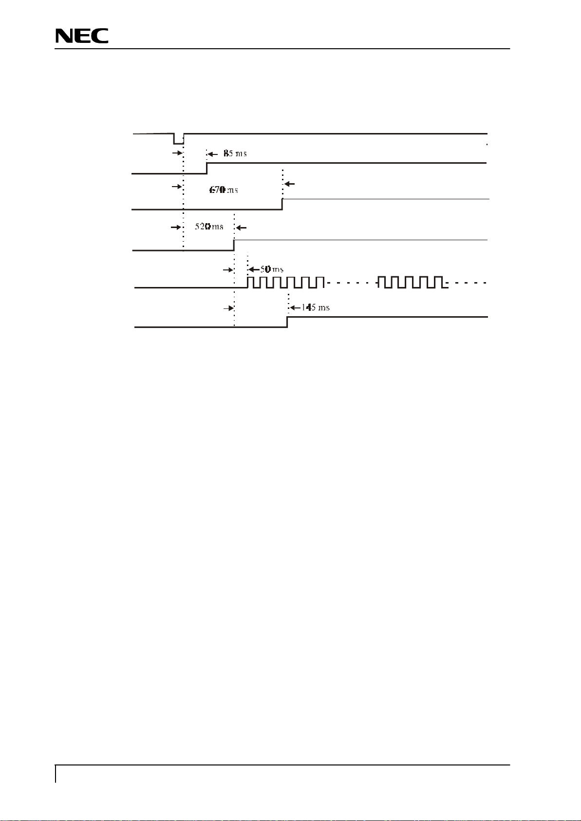
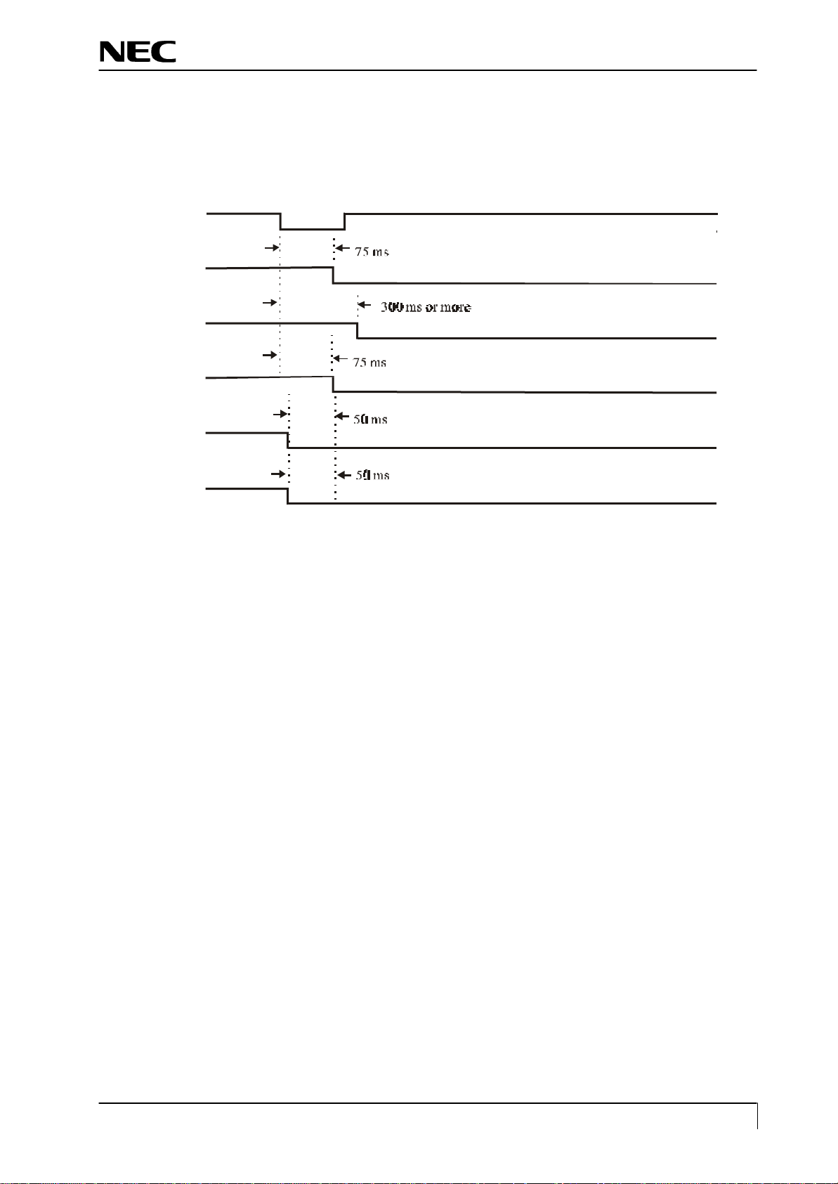
8.6 Power ON sequ ence
When the POWER switch is pressed, the POWER OFF signal is turned “H”. When this “H” potential is detected,
the CPU begins to establish the respective power supplies according to the sequence shown below.
8.7 Power OFF seq uence
When the POWER switch is pressed while the power supply is ON, the POWER ON signal is turned “H”. When
this “H” potential is detected, the CPU begins to turn off the respective power supplies according to the sequence
POWER
shown below.
LVCC
(Audio_EN)
LED
Panel_VCC
Backlight_EN
PCLK/DATA
Page 7Circuit Description
 Loading...