

Page 1
Global LCD Panel Exchange Center
TFT MONOCHROME LCD MODULE
NL256204AM15-01
www.panelook.com
NL256204AM15-01A
51cm (20.1 Type)
QSXGA
LVDS Interface (4 ports)
DATA SHEET
DOD-PD-0887 (4th edition)
This DATA SHEET is updated document from
DOD-PD-0561(3).
All information is subject to change without notice.
Please confirm the sales representative before
starting to design your system.
Document Number: DOD-PD-0887 (4th edition)
Published date: March 2005 CP(N)
One step solution for LCD / PDP / OLED panel application: Datasheet, inventory and accessory!
1
¤ NEC LCD Technologies, Ltd.
2003- 2005 All rights reserved.
www.panelook.com
Page 2
Global LCD Panel Exchange Center
No part of this document shall be copied in any form or by any means without the prior written consent
of NEC LCD Technologies, Ltd. (hereinafter called "NEC").
NEC does not assume any liability for infringement of patents, copyrights or other intellectual property
rights of third parties by or arising from use of a product described herein or any other liability arising
from use of such application. No license, express, implied or otherwise, is granted under any patents,
copyrights or other intellectual property rights of NEC or of others.
While NEC has been making continuous effort to enhance the reliability of its products, the possibility
of failures cannot be eliminated entirely. To minimize risks of damage to property or injury to person
arising from a failure in an NEC product, customers must incorporate sufficient safety measures in their
design, such as redundancy, fire-containment and anti-failure features.
www.panelook.com
NL256204AM15-01/01A
INTRODUCTION
NEC products are classified into the following three quality grades:
"Standard", "Special", "Specific"
The "Specific" quality grade applies only to applications developed based on a customer designated
"quality assurance program" for a specific application. The recommended applications of a product
depend on its quality grade, as indicated below. Customers must check the quality grade of each
application before using it in a particular application.
Standard: Computers, office equipment, communications equipment, test and measurement equipment,
audio and visual equipment, home electronic appliances, machine tools, personal electronic
equipment and industrial robots
Special: Transportation equipment (automobiles, trains, ships, etc.), traffic control systems, anti-disaster
systems, anti-crime systems, safety equipment and medical equipment (not specifically
designed for life support)
Specific: Military systems, aircraft, aerospace equipment, submersible repeaters, nuclear reactor control
systems, life support systems (medical equipment, etc.) and any other equipment
The quality grade of this product is "Standard" unless otherwise specified in this document. If
customers intend to use this product for applications other than those specified for "Standard" quality
grade, they should contact NEC sales representative in advance.
DATA SHEET DOD-PD-0887 (4th edition)
One step solution for LCD / PDP / OLED panel application: Datasheet, inventory and accessory!
2
www.panelook.com
Page 3
Global LCD Panel Exchange Center
INTRODUCTION ..........................................................................................................................................2
1. OUTLINE....................................................................................................................................................4
1.1 STRUCTURE AND PRINCIPLE...........................................................................................................4
1.2 APPLICATION.......................................................................................................................................4
1.3 FEATURES.............................................................................................................................................4
2. GENERAL SPECIFICATIONS ................................................................................................................5
3. BLOCK DIAGRAM ................................................................................................................................... 6
4. DETAILED SPECIFICATIONS ............................................................................................................... 7
4.1 MECHANICAL SPECIFICATIONS......................................................................................................7
4.2 ABSOLUTE MAXIMUM RATINGS ....................................................................................................7
4.3 ELECTRICAL CHARACTERISTICS................................................................................................... 8
4.3.1 LCD panel signal processing board ............................................................................................... 8
4.3.2 Inverter........................................................................................................................................... 9
4.3.3 Inverter current wave ..................................................................................................................... 9
4.3.4 Power supply voltage ripple.........................................................................................................10
4.3.5 Fuse.............................................................................................................................................. 10
4.4 POWER SUPPLY VOLTAGE SEQUENCE ........................................................................................ 11
4.4.1 LCD panel signal processing board ............................................................................................. 11
4.4.2 Inverter......................................................................................................................................... 11
4.5 CONNECTIONS AND FUNCTIONS FOR INTERFACE PINS.........................................................12
4.5.1 LCD panel signal processing board ............................................................................................. 12
4.5.2 Inverter......................................................................................................................................... 15
4.5.3 Positions of socket .......................................................................................................................15
4.6 LUMINANCE CONTROL................................................................................................................... 16
4.6.1 Luminance control methods.........................................................................................................16
4.6.2 Detail of PWM timing ................................................................................................................. 17
4.7 METHOD OF CONNECTION FOR LVDS TRANSMITTER............................................................18
4.8 DISPLAY GRAY SCALE AND INPUT DATA SIGNALS .................................................................. 20
4.9 INPUT SIGNAL TIMINGS.......................................................................................................
iming characteristics..................................................................................................................21
4.9.1 T
4.9.2 Input signal timing chart ..............................................................................................................21
4.10 LVDS DATA TRANSMISSION MODE ............................................................................................ 22
4.11 DISPLAY POSITIONS.......................................................................................................................23
4.12 PIXEL ARRANGNMENT .................................................................................................................24
4.13 TEN-bit LOOK UP TABLE FOR GAMMA ADJUSTMENT............................................................25
4.14 LUT SERIAL COMMUNICATION TIMINGS .................................................................................28
4.15 OPTICS...............................................................................................................................................30
4.15.1 Optical characteristics................................................................................................................30
4.15.2 Definition of contrast ratio......................................................................................................... 32
4.15.3 Definition of luminance uniformity...........................................................................................32
4.15.4 Definition of response times ...................................................................................................... 32
4.15.5 Definition of viewing angles......................................................................................................32
5. RELIABILITY TESTS.............................................................................................................................33
6. PRECAUTIONS .......................................................................................................................................34
6.1 MEANING OF CAUTION SIGNS ...................................................................................................... 34
6.2 CAUTIONS ..........................................................................................................................................34
6.3 ATTENTIONS ......................................................................................................................................34
6.3.1 Handling of the product ............................................................................................................... 34
6.3.2 Environment.................................................................................................................................35
6.3.3 Characteristics..............................................................................................................................36
6.3.4 Other ............................................................................................................................................36
7. OUTLINE DRAWINGS ........................................................................................................................... 37
www.panelook.com
NL256204AM15-01/01A
CONTENTS
...........21
DATA SHEET DOD-PD-0887 (4th edition)
One step solution for LCD / PDP / OLED panel application: Datasheet, inventory and accessory!
3
www.panelook.com
Page 4
Global LCD Panel Exchange Center
1. OUTLINE
1.1 STRUCTURE AND PRINCIPLE
Monochrome LCD module NL256204AM15-01 and NL256204AM15-01A are composed of the
amorphous silicon thin film transistor liquid crystal display (a-Si TFT LCD) panel structure with driver
LSIs for driving the TFT (Thin Film Transistor) array and a backlight.
The a-Si TFT LCD panel structure is injected liquid crystal material into a narrow gap between the TFT
array glass substrate and a monochrome-filter glass substrate.
Grayscale data signals from a host system (e.g. PC, signal generator, etc.) are modulated into best form
for active matrix system by a signal processing board, and sent to the driver LSIs which drive the
individual TFT arrays.
The TFT array as an electro-optical switch regulates the amount of transmitted light from the backlight
assembly, when it is controlled by data signals. Monochrome images are created by regulating the
amount of transmitted light through the TFT array.
www.panelook.com
NL256204AM15-01/01A
1.2 APPLICATION
x Monochrome monitor system
1.3 FEATURES
x Ultra-wide viewing angle (Adoption of Super Advanced -Super Fine TFT (SA-SFT))
x High luminance
x High contrast
x Low reflection
x High resolution
x 256 gray scales per 1 sub-pixel
x LVDS interface
x Adjustable gamma characteristics by using built-in 10-bit LUT (look up table)
x Selectable LVDS data input map
x Selectable LVDS data transmission mode
x Small foot print
x Incorporated direct type backlight
x Replaceable backlight unit and inverter
x Differences between NL256204AM15-01 and NL256204AM15-01A
Item NL256204AM15-01 NL256204AM15-01A
White chromaticity Wx, Wy = (0.255, 0.310) (typ.) Wx, Wy = (0.280, 0.304) (typ.)
Backlight unit
(Replaceable part)
DATA SHEET DOD-PD-0887 (4th edition)
201LHS07 201LHS08
One step solution for LCD / PDP / OLED panel application: Datasheet, inventory and accessory!
4
www.panelook.com
Page 5
Global LCD Panel Exchange Center
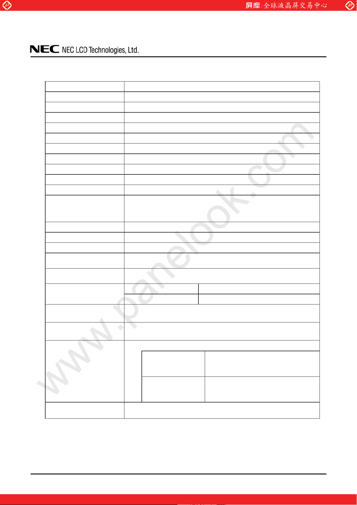
2. GENERAL SPECIFICATIONS
www.panelook.com
NL256204AM15-01/01A
Display area
Diagonal size of display
Drive system
Display gray scale
Pixel
Pixel arrangement
Sub-pixel pitch
Pixel pitch
Module size
Weig ht
Contrast ratio
Viewing angle
Designed viewing direction
Polarizer surface
Polarizer pencil-hardness
Response time
Luminance
White chromaticity
399.36 (H) u 319.488 (V) mm
51 cm (20.1 inches)
a-Si TFT active matrix
256 gray scales per 1 sub-pixel (8-bit) (766 gray scales per 1 pixel)
2,560 (H) u 2,048 (V) pixels (1 pixel consists of 3 sub pixels (LCR))
LCR Vertical stripe
0.052 (H) u 0.156 (V) mm
0.156 (H) u 0.156 (V) mm
423.4 (W) u 343.5 (H) u 43.5 (D) mm (typ.)
2,440 g (typ.)
600:1 (typ.)
t
At the contrast ratio
10:1
x Horizontal: Right side 85q (typ.), Left side 85q (typ.)
x Vertical: Up side 85q (typ.), Down side 85q (typ.)
Viewing angle with optimum grayscale (J=DICOM): normal axis Note1
Antiglare
2H (min.) [by JIS K5400]
Ton + Toff (10%
mo
90%)
30 ms (typ.)
At the maximum luminance control
850 cd/m
2
(typ.)
NL256204AM15-01 Wx, Wy = (0.255, 0.310) (typ.)
NL256204AM15-01A Wx, Wy = (0.280, 0.304) (typ.)
Signal system
Power supply voltage
4 ports LVDS interface
LCR 8-bit signals, Data enable signal (DE), Dot clock (CLK)
LCD panel signal processing board: 12.0V
Inverter: 12.0V
Direct light type: 12 cold cathode fluorescent lamps with an inverter
NL256204AM15-01
Backlight
NL256204AM15-01A
Power consumption
At checkered flag pattern and the maximum luminance control
49.2 W (typ.)
Note1: When the product luminance is 850cd/m
DATA SHEET DOD-PD-0887 (4th edition)
Replaceable parts
x Backlight unit: Type No.: 201LHS07
x Inverter: Type No.: 201PW121
Replaceable parts
x Backlight unit: Type No.: 201LHS08
x Inverter: Type No.: 201PW121
2
, the gamma characteristic is designed to J=DICOM.
5
One step solution for LCD / PDP / OLED panel application: Datasheet, inventory and accessory!
www.panelook.com
Page 6
Global LCD Panel Exchange Center
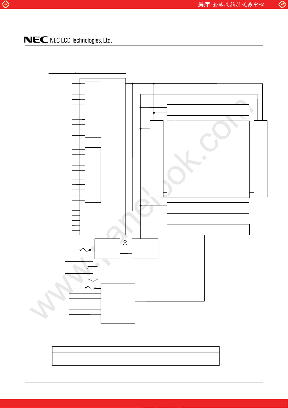
3. BLOCK DIAGRAM
Host LCD module (product)
DA0+/DA1+/DA2+/CKA+/DA3+/-
DB0+/DB1+/DB2+/CKB+/DB3+/-
DC0+/DC1+/DC2+/CKC+/DC3+/-
LVDS receiver
www.panelook.com
Controller
V-driver
2,048 lines
NL256204AM15-01/01A
H-driver
7,680 lines
TFT LCD panel
H: 2,560 u 3 (L, C, R)
V: 2,048
V-driver
DD0+/DD1+/DD2+/CKD+/DD3+/-
MOD>0:1@
BSEL>0:1@
CSR, CSL
SCLK
SDAT
VDD
GND
Note1, Note2
FG
Note1, Note2
VDDB
BRTC
BRTH
BRTI
BRTP
PWSEL
GNDB
Note1, Note2
Fuse
Fuse
LVDS receiver
Converter
DC/DC
H-driver
Backlight (Direct light type)
Power
supply for
drivers
Inverter
Note1: Connections between GND (Signal ground), FG (Frame ground) and GNDB (Inverter ground) in the
LCD module
GND - FG Not connected
GND - GNDB Not connected
FG - GNDB Not connected
Note2: GND, FG and GNDB must be connected to customer equipment’s ground, and it is recommended that
these grounds are connected together in customer equipment.
DATA SHEET DOD-PD-0887 (4th edition)
One step solution for LCD / PDP / OLED panel application: Datasheet, inventory and accessory!
6
www.panelook.com
Page 7
Global LCD Panel Exchange Center
4. DETAILED SPECIFICATIONS
4.1 MECHANICAL SPECIFICATIONS
Parameter Specification Unit
www.panelook.com
NL256204AM15-01/01A
Module size
Display area
Weight 2,440 (typ.), 2,600 (max.) g
423.4 r 1.0 (W) u 343.5 r 1.0 (H) u 43.5 r 1.0 (D)
Note1: See "7. OUTLINE DRAWINGS".
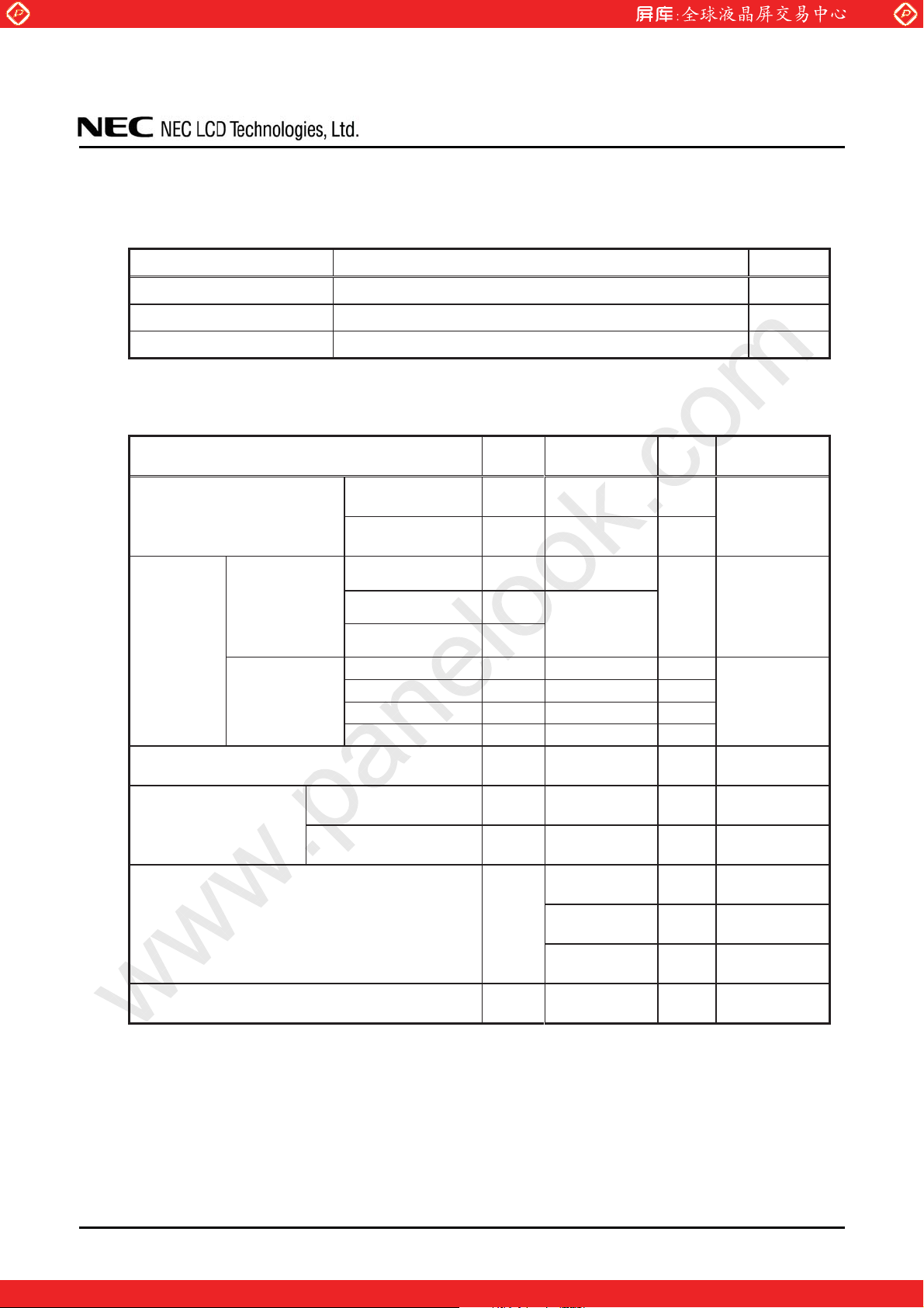
4.2 ABSOLUTE MAXIMUM RATINGS
Parameter Symbol Rating Unit Remarks
LCD panel signal
Power supply voltage
LCD panel signal
processing board
Input voltage
for signals
Inverter
processing board
Display signals
Function signal 1
Function signal 2
PWSEL signal VPSL -0.3 to +5.5 V
399.36 (H) u 319.488 (V)
VDD -0.3 to +15.0 V
Inverter VDDB -0.3 to +15.0 V
Note1
Note2
Note3
BRTI signal VBI -0.3 to +1.5 V
BRTP signal VBP -0.3 to +5.5 V
BRTC signal VBC -0.3 to +5.5 V
VD -0.3 to +3.6
VF1
-0.3 to +3.9
VF2
V
Note1 mm
Note1 mm
Ta = 25qC
Ta = 25qC
VDD=12.0V
Ta = 25qC
VDDB = 12.0V
Storage temperature Tst -20 to +60
Operating temperature
Relative humidity
Absolute humidity
Note6
Note6
Front surface TopF 0 to +55
Rear surface TopR 0 to +55
d 95
RH
AH
d 85
d 70
d 73
Note7
qC
qC
qC
%
%
%
g/m
3
-
Note4
Note5
Ta d 40qC
40 < Ta d 50qC
50 < Ta d 55qC
Ta > 55qC
Note1: DA0+/-, DA1+/-, DA2+/-, DA3+/-, CKA+/-, DB0+/-, DB1+/-, DB2+/-, DB3+/-, CKB+/-, DC0+/-,
DC1+/-, DC2+/-, DC3+/-, CKC+/-, DD0+/-, DD1+/-, DD2+/-, DD3+/-, CKD+/Note2: MOD0, MOD1, BSEL0, BSEL1
Note3: CSR, CSL, SCLK, SDAT
Note4: Measured at center of LCD panel surface (including self-heat)
Note5: Measured at center of LCD module's rear shield surface (including self-heat)
Note6: No condensation
Note7: Water amount at Ta = 55°C and RH = 70%
DATA SHEET DOD-PD-0887 (4th edition)
One step solution for LCD / PDP / OLED panel application: Datasheet, inventory and accessory!
7
www.panelook.com
Page 8
Global LCD Panel Exchange Center
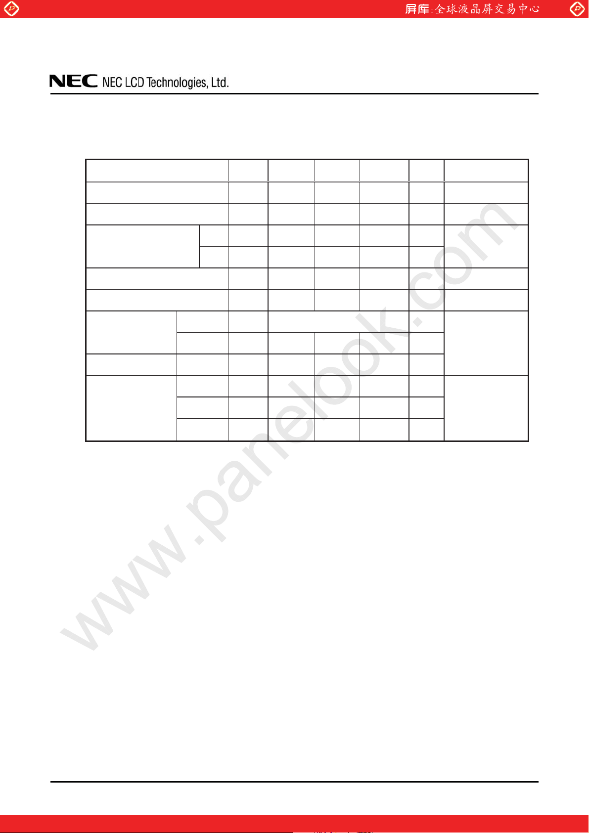
4.3 ELECTRICAL CHARACTERISTICS
4.3.1 LCD panel signal processing board
Parameter Symbol min. typ. max. Unit Remarks
Power supply voltage VDD 10.8 12.0 13.2 V -
Power supply current IDD -
Differential input threshold
voltage for Display signals
Input voltage swing VI 0 - 2.4 V Note4
www.panelook.com
NL256204AM15-01/01A
900
Note1
High VTH - - +100 mV
Low VTL -100 - - mV
1,800
Note2
mA
(Ta = 25qC)
at VDD = 12.0V,
Mode 0 is selected.
at VCM= 1.2V
Note3, Note4
Terminating resistance RT - 100 -
Input voltage for
Function signal 1
Input current for
Function signal 1
Input voltage for
Function signal 2
High VFH1 High must be Open. -
Low VFL1 0 - 0.8 V
Low IFL1 -10 - 10
High V+ - - 2.3 V
Low V- 0.5 - - V
Hysteresis VH 0.4 - - V
:
Note5
PA
Note6
Note1: Checkered flag pattern [by EIAJ ED-2522]
Note2: Pattern for maximum current
Note3: Common mode voltage for LVDS receiver
Note4: DA0+/-, DA1+/-, DA2+/-, DA3+/-, CKA+/-, DB0+/-, DB1+/-, DB2+/-, DB3+/-, CKB+/-,
DC0+/-, DC1+/-, DC2+/-, DC3+/-, CKC+/-, DD0+/-, DD1+/-, DD2+/-, DD3+/-, CKD+/-.
Note5: MOD0, MOD1, BSEL0, BSEL1
Note6: CSR, CSL, SCLK, SDAT
-
DATA SHEET DOD-PD-0887 (4th edition)
One step solution for LCD / PDP / OLED panel application: Datasheet, inventory and accessory!
8
www.panelook.com
Page 9
Global LCD Panel Exchange Center
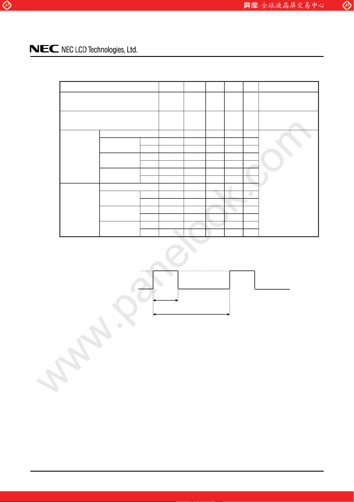
4.3.2 Inverter
Parameter Symbol min. typ. max. Unit Remarks
Power supply voltage VDDB 11.4 12.0 12.6 V -
Power supply current IDDB - 3,200 4,000
BRTI signal VBI 0 - 1.0 V
BRTP signal
Input voltage
for signals
Input current
for signals
BRTC signal
PWSEL signal
BRTI signal IBI -130 - -
BRTP signal
BRTC signal
PWSEL signal
www.panelook.com
NL256204AM15-01/01A
VDDB = 12.0V,
At the maximum
m$
luminance control
High VBPH 2.0 - 5.25 V
Low VBPL 0 - 0.8 V
High VBCH 2.0 - 5.25 V
Low VBCL 0 - 0.8 V
High VPSLH 2.0 - 5.25 V
Low VPSLL 0 - 0.8 V
P$
High IBPH - - 3.5 mA
Low IBPL -1.6 - - mA
High IBCH - - 440
Low IBCL -610 - -
High IPSLH - - 440
Low IPSLL -610 - -
P$
P$
P$
P$
(Ta = 25qC)
-
4.3.3 Inverter current wave
3,200 (mA) typ.
0 (A)
Duty
Luminance control frequency
Maximum luminance control: 100%
Minimum luminance control: 20%
Luminance control frequency: 285Hz (typ.)
Note1: Luminance control frequency indicate the input pulse frequency, when select the external pulse
control. See "4.6.2 Detail of PWM timing".
Note2: The power supply lines (VDDB and GNDB) have large ripple voltage (See "4.3.4 Power
supply voltage ripple".) during luminance control. There is the possibility that the ripple
voltage produces acoustic noise and signal wave noise in audio circuit and so on. Put a
capacitor (5,000 to 6,000PF) between the power supply lines (VDDB and GNDB) to reduce the
noise, if the noise occurred in the circuit.
DATA SHEET DOD-PD-0887 (4th edition)
One step solution for LCD / PDP / OLED panel application: Datasheet, inventory and accessory!
9
www.panelook.com
Page 10
Global LCD Panel Exchange Center
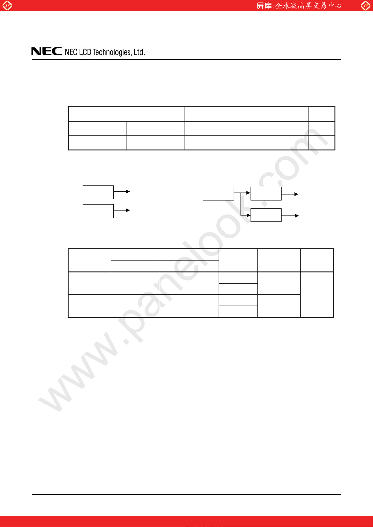
4.3.4 Power supply voltage ripple
This product works, even if the ripple voltage levels are beyond the permissible values as following
the table, but there might be noise on the display image.
www.panelook.com
NL256204AM15-01/01A
Power supply voltage
VDD 12.0 V
VDDB 12.0 V
Note1: The permissible ripple voltage includes spike noise.
Example of the power supply connection
a) Separate the power supply b) Put in the filter
Power
Power
VDD
VDDB
4.3.5 Fuse
Parameter
VDD
VDDB 0453007 Littelfuse Inc.
Type Supplier
FHC20 502AD
Note1: The power supply capacity should be more than the fusing current. If it is less than the fusing
current, the fuse may not blow in a short time, and then nasty smell, smoke and so on may
occur.
(Measure at input terminal of power supply)
Fuse
KAMAYA ELECTRIC
Co., Ltd.
Ripple voltage Note1
d 100
d 200
Power
Rating Fusing current Remarks
5A
24V
7A
125V
Filter
Filter
12.5A,
5s max.
14A,
5s max.
Unit
mVp-p
mVp-p
VDD
VDDB
Note1
ყ
DATA SHEET DOD-PD-0887 (4th edition)
One step solution for LCD / PDP / OLED panel application: Datasheet, inventory and accessory!
10
www.panelook.com
Page 11
Global LCD Panel Exchange Center
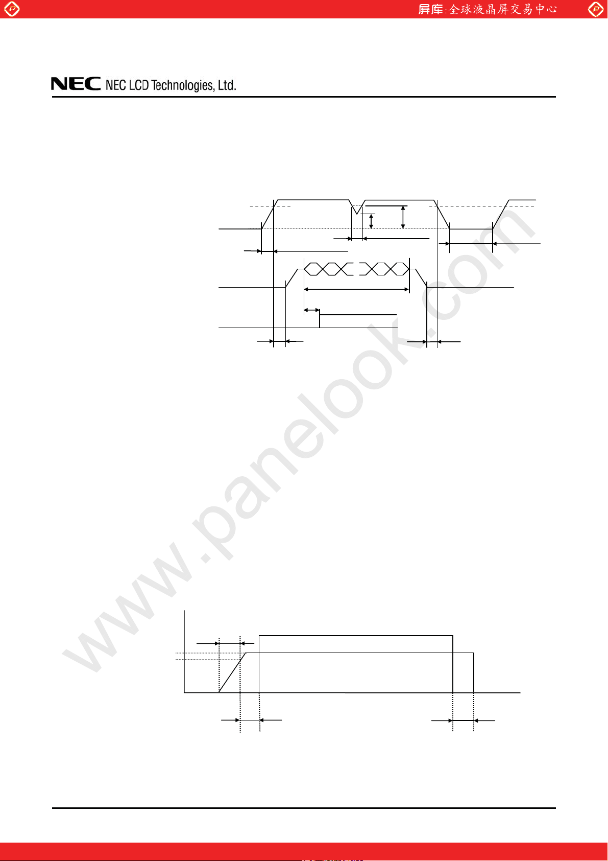
4.4 POWER SUPPLY VOLTAGE SEQUENCE
4.4.1 LCD panel signal processing board
www.panelook.com
NL256204AM15-01/01A
VDD
Note1, Note2
0V
VDD ON
10.8V
9.6V
VDD dip < 20ms
5ms < Tr < 80ms
VDD OFF
10.8V
VDD ON
10.8V
Tof f > 50ms
LVDS Signals *1,*2
Note3
0V
CSR, CSL, SCLK, SDAT
Note3
0V
10ms < t < 35ms
VALID period
tt20ms Note4
VALID period
0ms < t < 35ms
*1: DA0+/-, DA1+/-, DA2+/-, DA3+/-, CKA+/-, DB0+/-, DB1+/-, DB2+/-, DB3+/-, CKB+/-,
DC0+/-, DC1+/-, DC2+/-, DC3+/-, CKC+/-, DD0+/-, DD1+/-, DD2+/-, DD3+/-, CKD+/-
*2: LVDS signals should be measured at the terminal of 100: resistance.
Note1: In terms of voltage variation (voltage drop) while VDD rising edge is below 10.8V, a protection
circuit may work, and then this product may not work.
Note2: VDD should be 10.8V or more during VDD ON period.
Note3: LVDS signals and CSR, CSL, SCLK, SDAT must be Low or High-impedance, exclude the
VALID period (See above sequence diagram), in order to avoid that internal circuits is
damaged.
If some of signals are cut while this product is working, even if the signal input to it once again,
it might not work normally. If customer stops the display and function signals, they should be
cut VDD.
Note4: At the beginning of the serial communication mode, take 20ms or more after the LVDS signal
input.
4.4.2 Inverter
Voltage
12.0V
td800ms
BRTC
VDDB
11.4V
0<t
Note1: The inverter power supply voltage (VDDB) should be inputted within the valid period of LVDS
signals, in order to avoid unstable data display.
Note2: If tr is more than 800ms, the backlight will be turned off by a protection circuit for inverter.
Note3: When VDDB is 0V or BRTC is Low, PWSEL must be set to Low or Open.
DATA SHEET DOD-PD-0887 (4th edition)
One step solution for LCD / PDP / OLED panel application: Datasheet, inventory and accessory!
Time
0<t
11
www.panelook.com
Page 12
Global LCD Panel Exchange Center
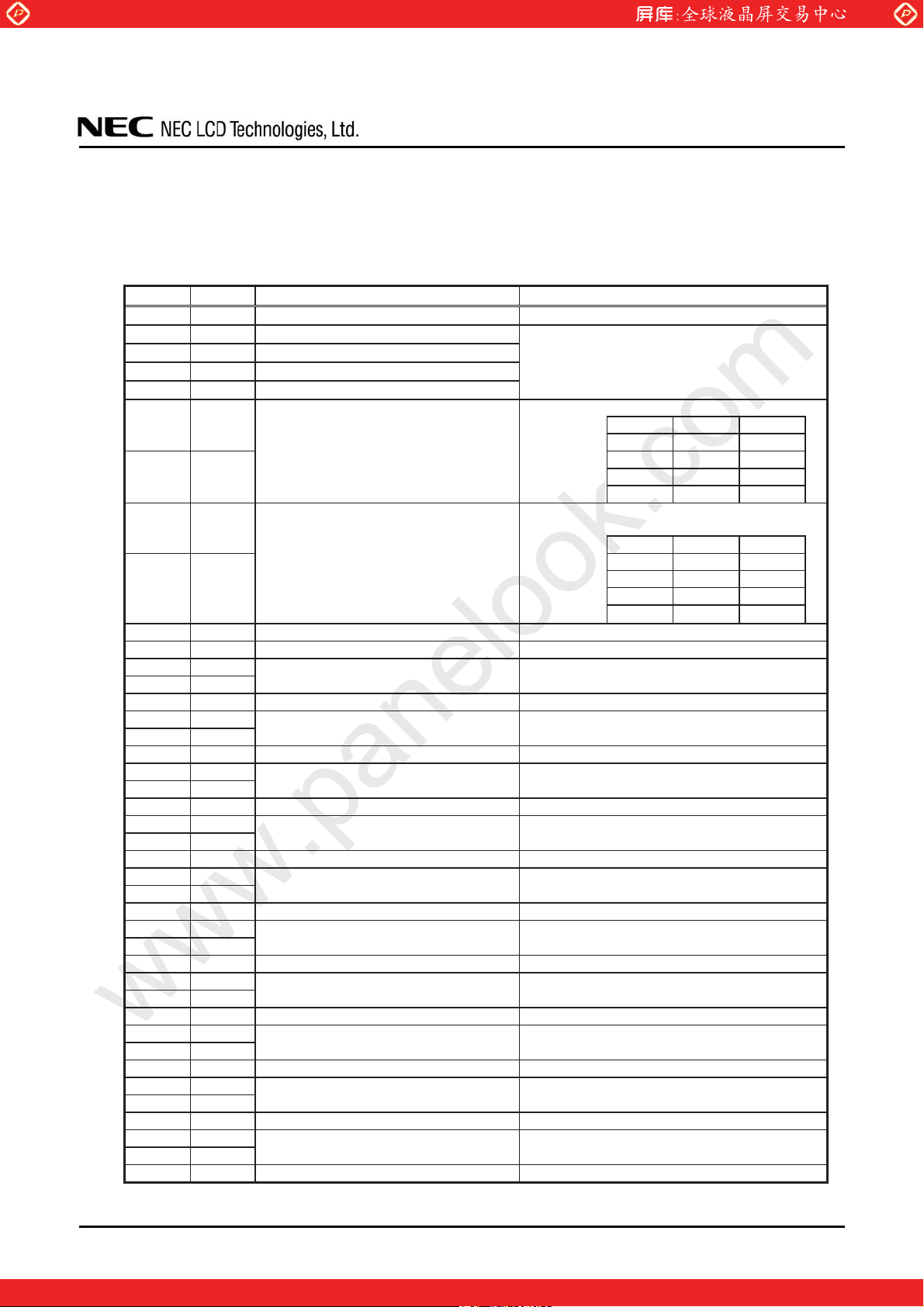
4.5 CONNECTIONS AND FUNCTIONS FOR INTERFACE PINS
4.5.1 LCD panel signal processing board
CN1 socket (LCD module side): FI-W41P-HF (Japan Aviation Electronics Industry Limited (JAE))
Adaptable plug: FI-W41S (Japan Aviation Electronics Industry Limited (JAE))
Pin No. Symbol Signal Remarks
1 GND Signal ground Note1
2 CSR Chip selection R
3 CSL Chip selection L
4 SCLK Serial Clock
5 SDAT Serial Data
6 MOD0
Selection of LVDS Data Transmission Mode
(Pull-up 25k:)
7 MOD1
8 BSEL0
Selection of LVDS data input map
(Pull-up 25k:)
9 BSEL1
10 RSVD Reserved Keep this pin Open.
11 GND Signal ground Note1
12 DB3+
13 DB314 GND Signal ground Note1
15 CKB+
16 CKB17 GND Signal ground Note1
18 DB2+
19 DB220 GND Signal ground Note1
21 DB1+
22 DB123 GND Signal ground Note1
24 DB0+
25 DB026 GND Signal ground Note1
27 DA3+
28 DA329 GND Signal ground Note1
30 CKA+
31 CKA32 GND Signal ground Note1
33 DA2+
34 DA235 GND Signal ground Note1
36 DA1+
37 DA138 GND Signal ground Note1
39 DA0+
40 DA041 GND Signal ground Note1
Pixel data B3 LVDS differential data input Note2
Pixel clock B LVDS differential clock input Note2
Pixel data B2 LVDS differential data input Note2
Pixel data B1 LVDS differential data input Note2
Pixel data B0 LVDS differential data input Note2
Pixel data A3 LVDS differential data input Note2
Pixel clock A LVDS differential clock input Note2
Pixel data A2 LVDS differential data input Note2
Pixel data A1 LVDS differential data input Note2
Pixel data A0 LVDS differential data input Note2
www.panelook.com
NL256204AM15-01/01A
LUT communication control signal
See "4.13 TEN-bit LOOK UP TABLE FOR
GAMMA ADJUSTMENT".
See "4.10 LVDS DATA TRANSMISSION MODE".
MOD0 MOD1 Mode
Open Open 0
Open Low 1
Low Open Reserved
Low Low 0
See "4.7 METHOD OF CONNECTION FOR
LVDS TRANSMITTER".
BSEL0 BSEL1 Mode
Open Open A
Open Low B
Low Open C
Low Low A
DATA SHEET DOD-PD-0887 (4th edition)
One step solution for LCD / PDP / OLED panel application: Datasheet, inventory and accessory!
12
www.panelook.com
Page 13
Global LCD Panel Exchange Center
Note1: All GND terminals should be used without any non-connected lines.
Note2: Twist pair wires with 100: (Characteristic impedance) should be connected between LCD panel
signal processing board and LVDS transmitter.
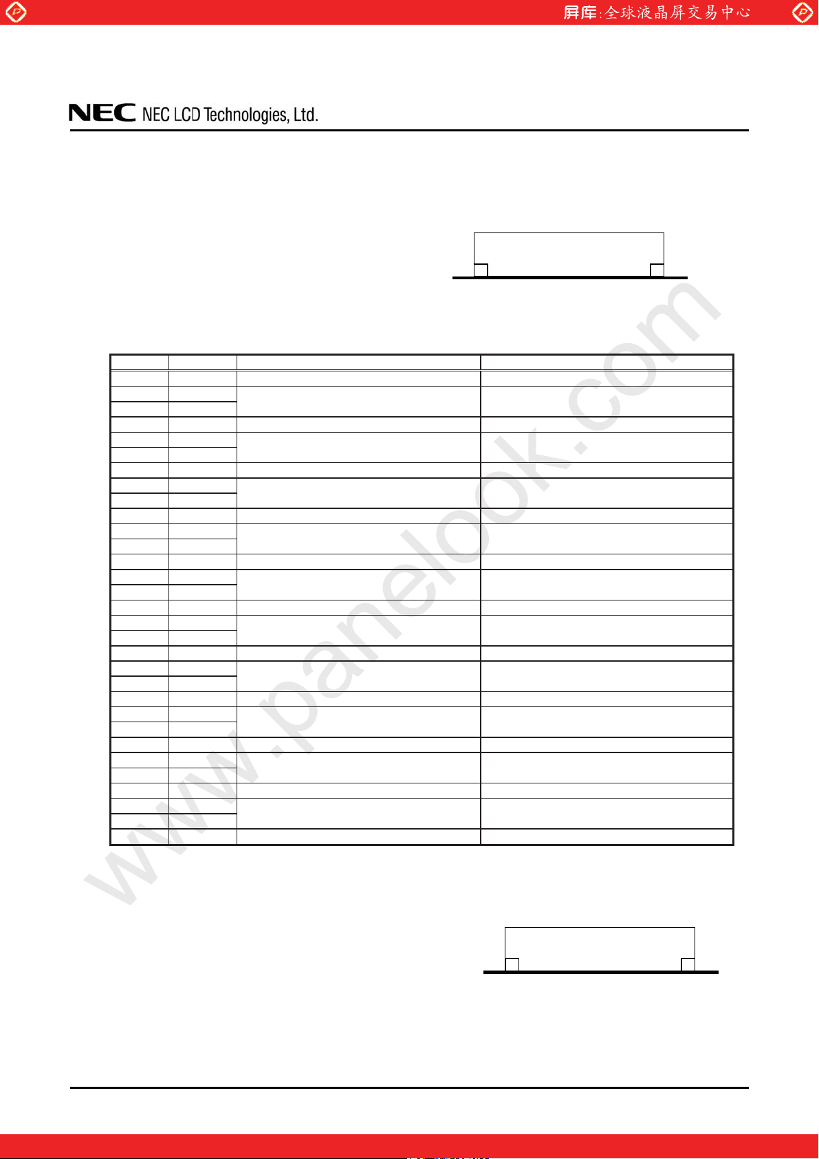
CN2 socket (LCD module side): FI-W31P-HF (Japan Aviation Electronics Industry Limited (JAE))
Adaptable plug: FI-W31S (Japan Aviation Electronics Industry Limited (JAE))
Pin No. Symbol Signal Remarks
1 GND Signal ground Note1
2 DD3+
3 DD34 GND Signal ground Note1
5 CKD+
6 CKD7 GND Signal ground Note1
8 DD2+
9 DD210 GND Signal ground Note1
11 DD1+
12 DD113 GND Signal ground Note1
14 DD0+
15 DD016 GND Signal ground Note1
17 DC3+
18 DC319 GND Signal ground Note1
20 CKC+
21 CKC22 GND Signal ground Note1
23 DC2+
24 DC225 GND Signal ground Note1
26 DC1+
27 DC128 GND Signal ground Note1
29 DC0+
30 DC031 GND Signal ground Note1
Pixel data D3 LVDS differential data input Note2
Pixel clock D LVDS differential clock input Note2
Pixel data D2 LVDS differential data input Note2
Pixel data D1 LVDS differential data input Note2
Pixel data D0 LVDS differential data input Note2
Pixel data C3 LVDS differential data input Note2
Pixel clock C LVDS differential clock input Note2
Pixel data C2 LVDS differential data input Note2
Pixel data C1 LVDS differential data input Note2
Pixel data C0 LVDS differential data input Note2
Note1: All GND terminals should be used without any non-connected lines.
Note2: Twist pair wires with 100: (Characteristic impedance) should be connected between LCD panel
signal processing board and LVDS transmitter.
www.panelook.com
NL256204AM15-01/01A
CN1: Figure of socket
41 39 ……… 3 1
40 38 ……… 4 2
CN2: Figure of socket
31 29 ……… 3 1
30 28 ……… 4 2
DATA SHEET DOD-PD-0887 (4th edition)
One step solution for LCD / PDP / OLED panel application: Datasheet, inventory and accessory!
13
www.panelook.com
Page 14
Global LCD Panel Exchange Center
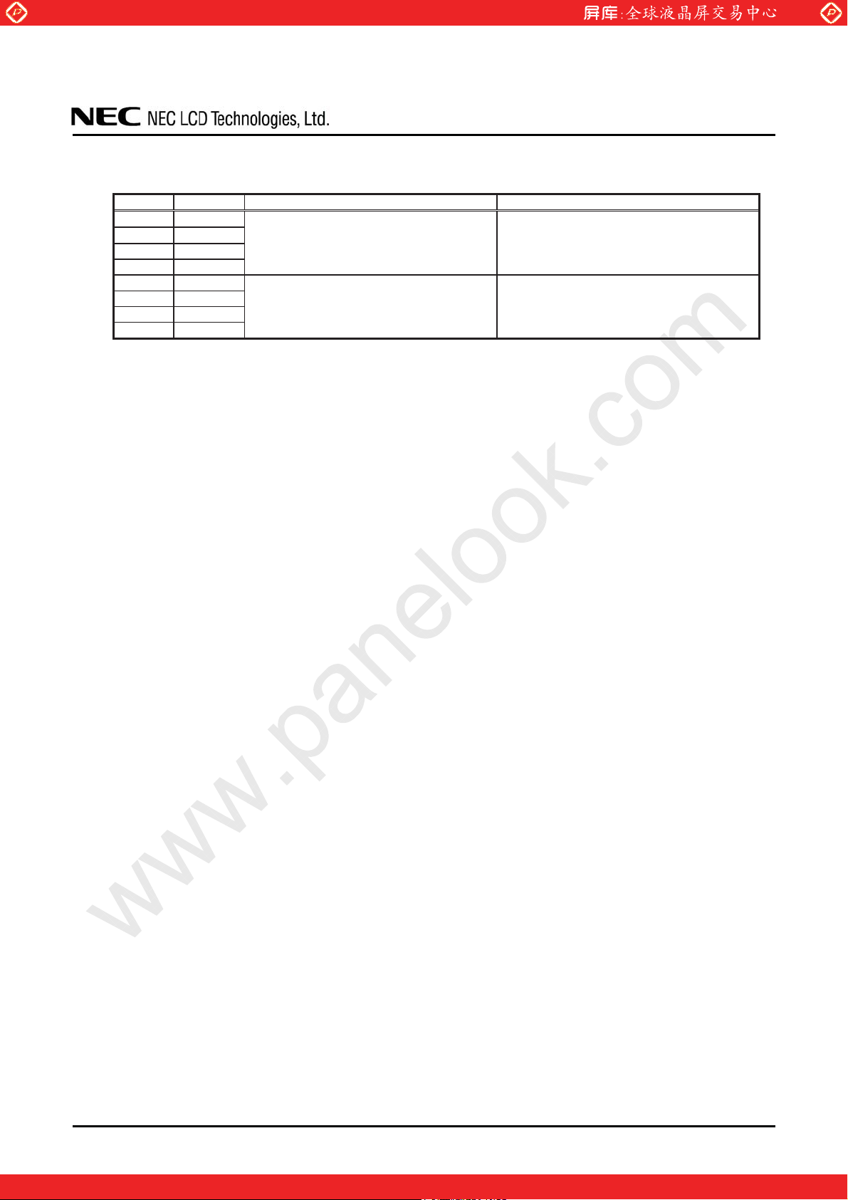
CN3 socket (LCD module side): IL-Z-8PL-SMTY (Japan Aviation Electronics Industry Limited (JAE))
Adaptable plug: IL-Z-8S-S125C (Japan Aviation Electronics Industry Limited (JAE))
Pin No. Symbol Function Description
1 VDD
2 VDD
3 VDD
4 VDD
5 GND
6 GND
7 GND
8 GND
Power supply Note1
Signal ground Note1
Note1: All VDD and GND terminals should be used without any non-connected lines.
www.panelook.com
NL256204AM15-01/01A
DATA SHEET DOD-PD-0887 (4th edition)
One step solution for LCD / PDP / OLED panel application: Datasheet, inventory and accessory!
14
www.panelook.com
Page 15
Global LCD Panel Exchange Center
4.5.2 Inverter
www.panelook.com
NL256204AM15-01/01A
CN201 socket (LCD module side): DF3Z-8P-2H (HIROSE ELECTRIC Co,.Ltd.)
Adaptable plug: DF3-8S-2C (HIROSE ELECTRIC Co,.Ltd.)
Pin No. Symbol Function Description
1 GNDB
2 GNDB
3 GNDB
4 GNDB
5 VDDB
6 VDDB
7 VDDB
8 VDDB
Inverter ground Note1
Power supply Note1
Note1: All VDDB and GNDB terminals should be used without any non-connected lines.
CN202 socket (LCD module side): IL-Z-9PL-SMTYE (Japan Aviation Electronics Industry Limited (JAE))
Adaptable plug: IL-Z-9S-S125C3 (Japan Aviation Electronics Industry Limited (JAE))
Pin No. Symbol Function Description
1 GNDB
2 GNDB
3 N.C. - Keep this pin Open.
4 BRTC
5 BRTH
6 BRTI
7 BRTP BRTP signal
8 GNDB Inverter ground Note1
9 PWSEL Selection of luminance control signal method
Inverter ground Note1
Backlight ON/OFF control signal
Luminance control terminal
High or Open: Backlight ON
Low: Backlight OFF
See "4.6 LUMINANCE CONTROL".
See "4.6 LUMINANCE CONTROL ".
Note2
Note1: All GNDB terminals should be used without any non-connected lines.
Note2: When VDDB is 0V or BRTC is Low, PWSEL must be set to Low or Open.
ყ
ყ
ყ
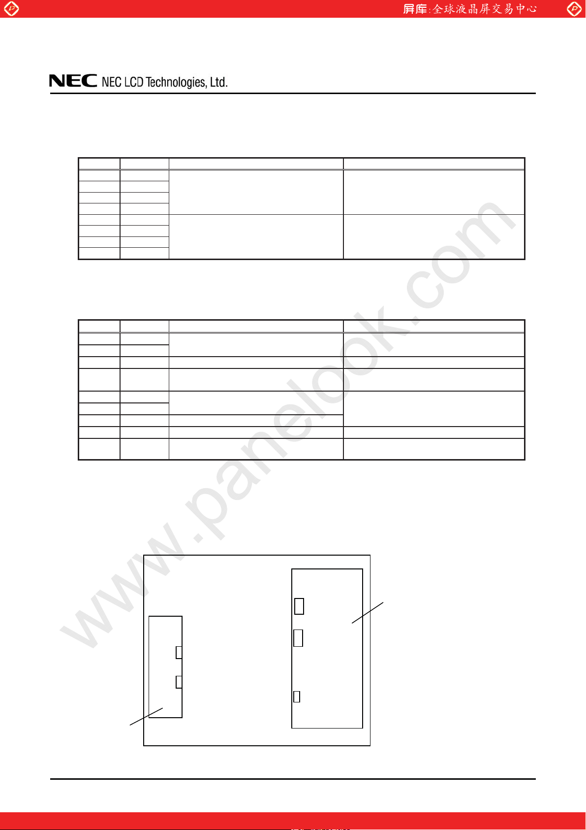
4.5.3 Positions of socket
1
CN202
9
m Insert direction
10
CN201
1
Inverter
Rear side
41
CN1
Insert directiono
Insert directiono
DATA SHEET DOD-PD-0887 (4th edition)
1
31
CN2
1
8
CN3
1
LCD panel signal processing board
15
One step solution for LCD / PDP / OLED panel application: Datasheet, inventory and accessory!
www.panelook.com
Page 16
Global LCD Panel Exchange Center
4.6 LUMINANCE CONTROL
4.6.1 Luminance control methods
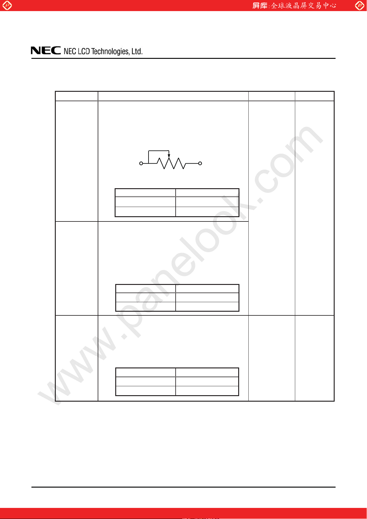
Method Adjustment and luminance ratio PWSEL terminal BRTP terminal
x Adjustment
The variable resistor (R) for luminance control should be 10k:
r5%, B curve, 1/10W. Minimum point of the resistance is the
minimum luminance and maximum point of the resistance is the
maximum luminance.
The resistor (R) must be connected between BRTH-BRTI
Variable resistor
control
terminals.
www.panelook.com
NL256204AM15-01/01A
Note1
Voltage control
Note1
Pulse width
modulation
Note1
Note2
BRTH
x Luminance ratio Note3
Resistance Luminance ratio
0 :
10 k:
x Adjustment
Voltage control method works, when BRTH terminal is 0V and
VBI voltage is input between BRTI-BRTH terminals. This
control method can carry out continuation adjustment of
luminance.
Luminance is the maximum when BRTI terminal is Open.
x Luminance ratio Note3
BRTI Voltage (VBI) Luminance ratio
0V 30% (Min. Luminance)
1.0V 100% (Max. Luminance)
x Adjustment
Pulse width modulation (PWM) method works, when PWSEL
terminal is Low and PWM signal (BRTP signal) is input into
BRTP terminal. The luminance is controlled by duty ratio of
BRTP signal.
x Luminance ratio Note3
Duty ratio Note4 Luminance ratio
0.2 20% (Min. Luminance)
1.0 100% (Max. Luminance)
R
BRTI
30% (Min. Luminance)
100% (Max. Luminance)
High or Open Open
Low BRTP signal
Note1: In case of the variable resistor control method and the voltage control method, noises may
appear on the display image depending on the input signals timing for LCD panel signal
processing board.
Use PWM method, if interference noises appear on the display image!
Note2: The inverter will stop working, when BRTP signal is fixed to Low while BRTC signal is High
or Open. Then the backlight will not turn on anymore, even if BRTP signal is input again. This
is not out of order. Backlight inverter will start to work when power is supplied again.
Note3: These data are the target values.
Note4: See "4.6.2 Detail of PWM timing".
DATA SHEET DOD-PD-0887 (4th edition)
One step solution for LCD / PDP / OLED panel application: Datasheet, inventory and accessory!
16
www.panelook.com
Page 17
Global LCD Panel Exchange Center
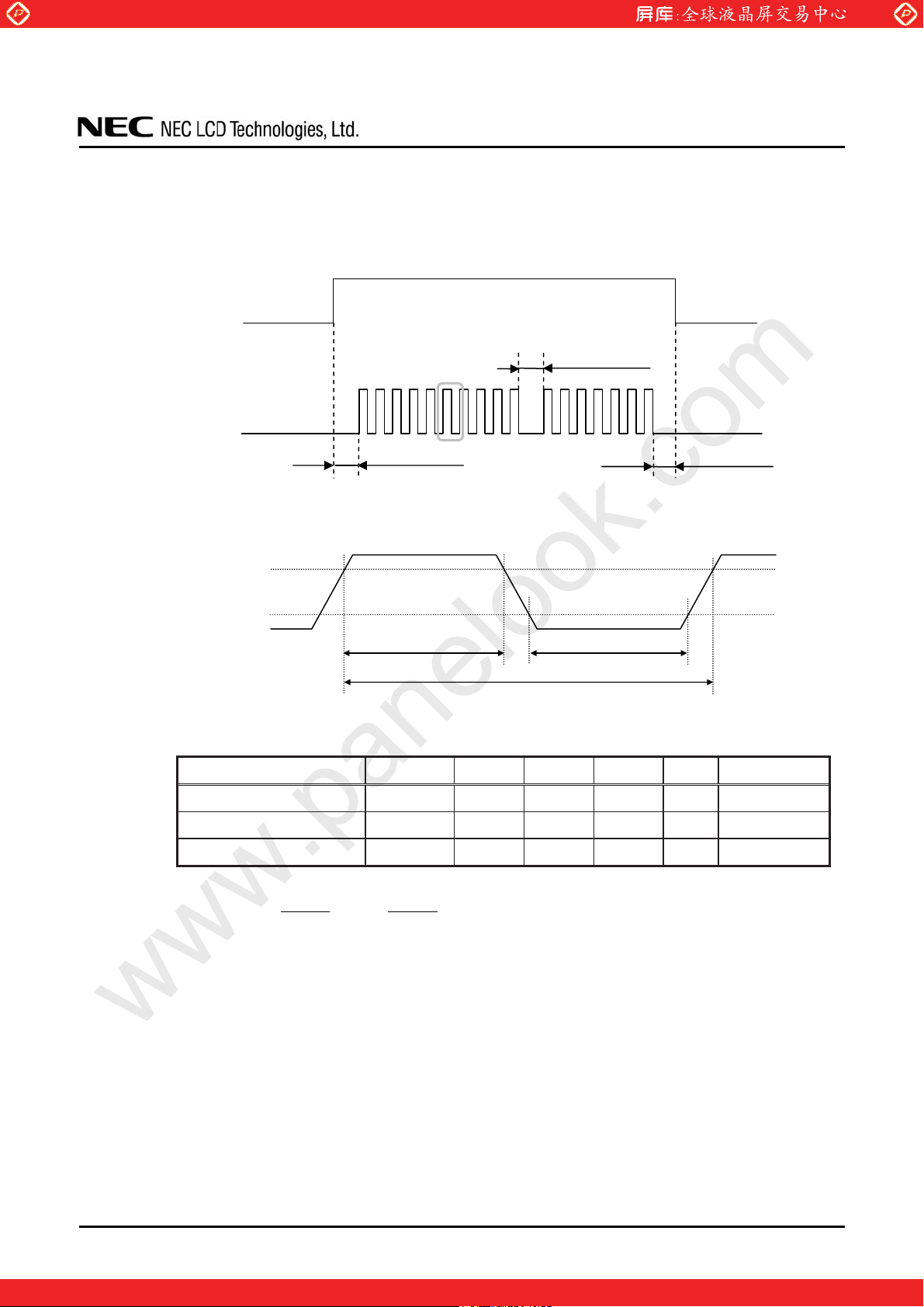
4.6.2 Detail of BRTP timing
(1) Timing diagrams
x Outline chart
BRTC
www.panelook.com
NL256204AM15-01/01A
BRTP
x Detail of A part
VBPH
BRTP
VBPL
(2) Each parameter
Parameter Symbol min. typ. max. Unit Remarks
Luminance control frequency FL 185 - 325 Hz Note1, Note2
A
0 d tPWL d 50ms
tPWH
0 d tPWL d 50ms
0 d tPWL d 50ms
tPWL
tPW
Duty ratio DL 0.2 - 1.0 - Note1, Note3
Low period tPWL 0 - 50 ms Note4
Note1: Definition of parameters is as follows.
FL =
1
tPW
DL =
tPWH
tPW
Note2: See the following formula for luminance control frequency.
Luminance control frequency = 1/tv u (n+0.25) [or (n + 0.75)]
n = 1, 2, 3 · · · · · ·
tv: Vertical cycle (See "4.9.1 Timing characteristics".)
The interference noise of luminance control frequency and input signal frequency for
LCD panel signal processing board may appear on a display. Set up luminance control
frequency so that the interference noise does not appear!
Note3: See "4.6.1 Luminance control methods".
Note4: If tPWL is more than 50ms, the backlight will be turned off by a protection circuit for
inverter.
DATA SHEET DOD-PD-0887 (4th edition)
17
One step solution for LCD / PDP / OLED panel application: Datasheet, inventory and accessory!
www.panelook.com
Page 18
Global LCD Panel Exchange Center
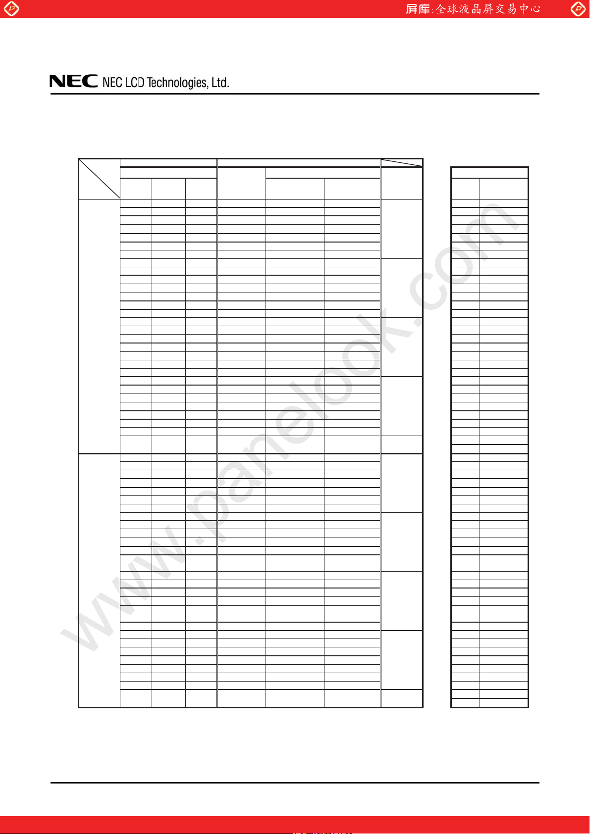
4.7 METHOD OF CONNECTION FOR LVDS TRANSMITTER
LVDS data input map is selectable by BSEL0 and BSEL1 terminal.
Bit mapping Transmitter Pin Assignment
BSEL[1:0] Note1, Note2 Dual type LVDS TX CN1
Pixel data
A
Pixel data
B
[H:H],
[L:L]
Mode A Mode B Mode C
LA2 LA7 LA0 TA0 R12 R10
LA3 LA6 LA1 TA1 R13 R11 Note3
LA4 LA5 LA2 TA2 R14 R12 ATA-
LA5 LA4 LA3 TA3 R15 R13 ATA+
LA6 LA3 LA4 TA4 R16 R14
LA7 LA2 LA5 TA5 R17 R15
CA2 CA7 CA0 TA6 G12 G10
CA3 CA6 CA1 TB0 G13 G11
CA4 CA5 CA2 TB1 G14 G12
CA5 CA4 CA3 TB2 G15 G13 ATB-
CA6 CA3 CA4 TB3 G16 G14 ATB+
CA7 CA2 CA5 TB4 G17 G15
RA2 RA7 RA0 TB5 B12 B10
RA3 RA6 RA1 TB6 B13 B11
RA4 RA5 RA2 TC0 B14 B12
RA5 RA4 RA3 TC1 B15 B13
RA6 RA3 RA4 TC2 B16 B14 ATC-
RA7 RA2 RA5 TC3 B17 B15 ATC+
Hsync Hsync Hsync TC4 HSYNC HSYNC
Vsync Vsync Vsync TC5 VSYNC VSYNC
LA0 LA1 LA6 TD0 R10 R16
LA1 LA0 LA7 TD1 R11 R17
CA0 CA1 CA6 TD2 G10 G16 ATD-
CA1 CA0 CA7 TD3 G11 G17 ATD+
RA0 RA1 RA6 TD4 B10 B16
RA1 RA0 RA7 TD5 B11 B17
N.C. N.C. N.C. TD6 - -
CLK CLK CLK CLK CLK CLK
LB2 LB7 LB0 TA0 R22 R20
LB3 LB6 LB1 TA1 R23 R21
LB4 LB5 LB2 TA2 R24 R22 BTA-
LB5 LB4 LB3 TA3 R25 R23 BTA+
LB6 LB3 LB4 TA4 R26 R24
LB7 LB2 LB5 TA5 R27 R25
CB2 CB7 CB0 TA6 G22 G20
CB3 CB6 CB1 TB0 G23 G21
CB4 CB5 CB2 TB1 G24 G22
CB5 CB4 CB3 TB2 G25 G23 BTB-
CB6 CB3 CB4 TB3 G26 G24 BTB+
CB7 CB2 CB5 TB4 G27 G25
RB2 RB7 RB0 TB5 B22 B20
RB3 RB6 RB1 TB6 B23 B21
RB4 RB5 RB2 TC0 B24 B22
RB5 RB4 RB3 TC1 B25 B23
RB6 RB3 RB4 TC2 B26 B24 BTC-
RB7 RB2 RB5 TC3 B27 B25 BTC+
Hsync Hsync Hsync TC4 HSYNC HSYNC
Vsync Vsync Vsync TC5 VSYNC VSYNC
LB0 LB1 LB6 TD0 R20 R26
LB1 LB0 LB7 TD1 R21 R27
CB0 CB1 CB6 TD2 G20 G26 BTD-
CB1 CB0 CB7 TD3 G21 G27 BTD+
RB0 RB1 RB6 TD4 B20 B26
RB1 RB0 RB7 TD5 B21 B27
N.C. N.C. N.C. TD6 - -
CLK CLK CLK CLK CLK CLK
[H:L] [L:H]
DE DE DE TC6 DE DE
DE DE DE TC6 DE DE
www.panelook.com
Single type
LVDS Tx
THine
THC63LVD823
NS
DS90C387
NL256204AM15-01/01A
Output
Connector
ATC L K -
ATC L K +
BTCLKBTCLK+
Pin No. Signal name
40 DA0-
o
39 DA0+
o
37 DA1-
o
36 DA1+
o
34 DA2-
o
33 DA2+
o
28 DA3-
o
27 DA3+
o
31 CKA-
o
30 CKA+
o
25 DB0-
o
24 DB0+
o
22 DB1-
o
21 DB1+
o
19 DB2-
o
18 DB2+
o
13 DB3-
o
12 DB3+
o
16 CKB-
o
15 CKB+
o
DATA SHEET DOD-PD-0887 (4th edition)
One step solution for LCD / PDP / OLED panel application: Datasheet, inventory and accessory!
18
www.panelook.com
Page 19
Global LCD Panel Exchange Center
www.panelook.com
NL256204AM15-01/01A
Pixel data
C
Pixel data
D
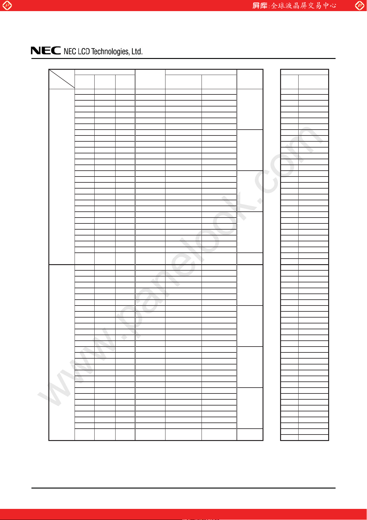
BSEL[1:0] Note1, Note2 Dual type LVDS TX CN2
[H:H],
[L:L]
Mode A Mode B Mode C
LC2 LC7 LC0 TA0 R12 R10
LC3 LC6 LC1 TA1 R13 R11 Note3
LC4 LC5 LC2 TA2 R14 R12 CTA-
LC5 LC4 LC3 TA3 R15 R13 CTA+
LC6 LC3 LC4 TA4 R16 R14
LC7 LC2 LC5 TA5 R17 R15
CC2 CC7 CC0 TA6 G12 G10
CC3 CC6 CC1 TB0 G13 G11
CC4 CC5 CC2 TB1 G14 G12
CC5 CC4 CC3 TB2 G15 G13 CTB-
CC6 CC3 CC4 TB3 G16 G14 CTB+
CC7 CC2 CC5 TB4 G17 G15
RC2 RC7 RC0 TB5 B12 B10
RC3 RC6 RC1 TB6 B13 B11
RC4 RC5 RC2 TC0 B14 B12
RC5 RC4 RC3 TC1 B15 B13
RC6 RC3 RC4 TC2 B16 B14 CTC-
RC7 RC2 RC5 TC3 B17 B15 CTC+
Hsync Hsync Hsync TC4 HSYNC HSYNC
Vsync Vsync Vsync TC5 VSYNC VSYNC
LC0 LC1 LC6 TD0 R10 R16
LC1 LC0 LC7 TD1 R11 R17
CC0 CC1 CC6 TD2 G10 G16 CTD-
CC1 CC0 CC7 TD3 G11 G17 CTD+
RC0 RC1 RC6 TD4 B10 B16
RC1 RC0 RC7 TD5 B11 B17
N.C. N.C. N.C. TD6 - -
CLK CLK CLK CLK CLK CLK
LD2 LD7 LD0 TA0 R22 R20
LD3 LD6 LD1 TA1 R23 R21
LD4 LD5 LD2 TA2 R24 R22 DTA-
LD5 LD4 LD3 TA3 R25 R23 DTA+
LD6 LD3 LD4 TA4 R26 R24
LD7 LD2 LD5 TA5 R27 R25
CD2 CD7 CD0 TA6 G22 G20
CD3 CD6 CD1 TB0 G23 G21
CD4 CD5 CD2 TB1 G24 G22
CD5 CD4 CD3 TB2 G25 G23 DTB-
CD6 CD3 CD4 TB3 G26 G24 DTB+
CD7 CD2 CD5 TB4 G27 G25
RD2 RD7 RD0 TB5 B22 B20
RD3 RD6 RD1 TB6 B23 B21
RD4 RD5 RD2 TC0 B24 B22
RD5 RD4 RD3 TC1 B25 B23
RD6 RD3 RD4 TC2 B26 B24 DTC-
RD7 RD2 RD5 TC3 B27 B25 DTC+
Hsync Hsync Hsync TC4 HSYNC HSYNC
Vsync Vsync Vsync TC5 VSYNC VSYNC
LD0 LD1 LD6 TD0 R20 R26
LD1 LD0 LD7 TD1 R21 R27
CD0 CD1 CD6 TD2 G20 G26 DTD-
CD1 CD0 CD7 TD3 G21 G27 DTD+
RD0 RD1 RD6 TD4 B20 B26
RD1 RD0 RD7 TD5 B21 B27
N.C. N.C. N.C. TD6 - -
CLK CLK CLK CLK CLK CLK
[H:L] [L:H]
DE DE DE TC6 DE DE
DE DE DE TC6 DE DE
Single type
LVDS Tx
THine
THC63LVD823
NS
DS90C387
Output
Connector
CTCLKCTCLK+
DTCLK-
DTCLK+
Pin No. Signal name
o
30 DC0-
o
29 DC0+
o
27 DC1-
o
26 DC1+
o
24 DC2-
o
23 DC2+
o
18 DC3-
o
17 DC3+
o
21 CKC-
o
20 CKC+
o
15 DD0-
o
14 DD0+
o
12 DD1-
o
11 DD1+
o
o
o
o
o
o
9 DD2-
8 DD2+
3 DD3-
2 DD3+
6 CKD-
5 CKD+
Note1: High must be Open.
Note2: Do not change the setting of BSEL0 and BSEL1 during VDD ON period.
Note3: Twist pair wires with 100: (Characteristic impedance) should be connected between LCD
panel signal processing board and LVDS transmitter.
DATA SHEET DOD-PD-0887 (4th edition)
One step solution for LCD / PDP / OLED panel application: Datasheet, inventory and accessory!
19
www.panelook.com
Page 20
Global LCD Panel Exchange Center
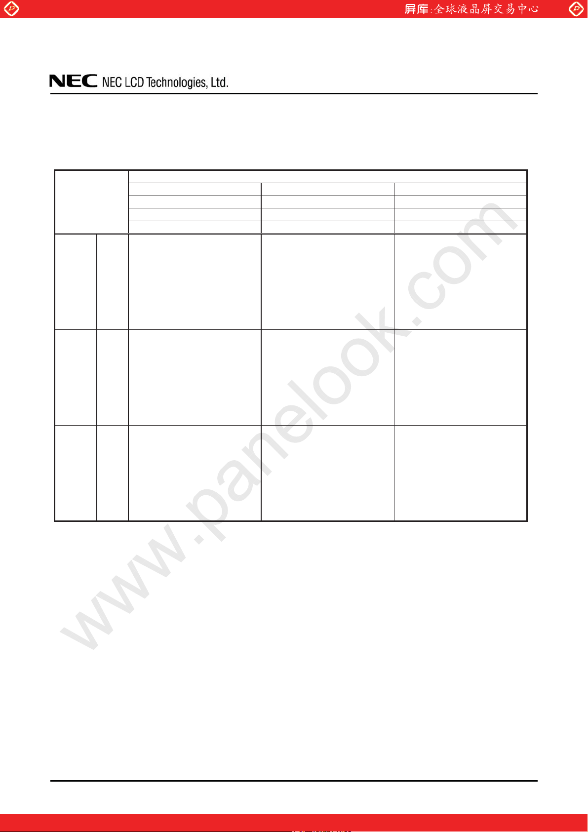
4.8 DISPLAY GRAY SCALE AND INPUT DATA SIGNALS
This product can display 256 gray scales in each LCR sub-pixel and 766 gray scales per 1 pixel. Also the
relation between display gray scale and input data signals is as the following table.
LA7 LA6 LA5 LA4 LA3 LA2 LA1 LA0 CA7 CA6 CA5 CA4 CA3 CA2 CA1 CA0 RA7 RA6 RA5 RA4 RA3 RA2 RA1 RA0
Display gray scale
LB7 LB6 LB5 LB4 LB3 LB2 LB1 LB0 CB7 CB6 CB5 CB4 CB3 CB2 CB1 CB0 RB7 RB6 RB5 RB4 RB3 RB2 RB1 RB0
LC7 LC6 LC5 LC4 LC3 LC2 LC1 LC0 CC7 CC6 CC5 CC4 CC3 CC2 CC1 CC0 RC7 RC6 RC5 RC4 RC3 RC2 RC1 RC0
LD7 LD6 LD5 LD4 LD3 LD2 LD1 LD0 CD7 CD6 CD5 CD4 CD3 CD2 CD1 CD0 RD7 RD6 RD5 RD4 RD3 RD2 RD1 RD0
Black
0 0 0 0 0 0 0 0
0 0 0 0 0 0 0 1
0 0 0 0 0 0 1 0
n
p
:
:
1 1 1 1 1 1 0 1
1 1 1 1 1 1 1 0
1 1 1 1 1 1 1 1
0 0 0 0 0 0 0 0
Left sub-pixel gray scale
dark
bright
White
Black
0 0 0 0 0 0 0 0
dark
bright
0 0 0 0 0 0 0 0
n
p
:
:
0 0 0 0 0 0 0 0
0 0 0 0 0 0 0 0
Center sub-pixel gray scale
White
Black
0 0 0 0 0 0 0 0
0 0 0 0 0 0 0 0
0 0 0 0 0 0 0 0
dark
bright
0 0 0 0 0 0 0 0
n
p
:
:
0 0 0 0 0 0 0 0
0 0 0 0 0 0 0 0
Right sub-pixel gray scale
White
0 0 0 0 0 0 0 0
www.panelook.com
Data signal (0: Low level, 1: High level)
0 0 0 0 0 0 0 0
0 0 0 0 0 0 0 0
0 0 0 0 0 0 0 0
:
:
0 0 0 0 0 0 0 0
0 0 0 0 0 0 0 0
0 0 0 0 0 0 0 0
0 0 0 0 0 0 0 0
0 0 0 0 0 0 0 1
0 0 0 0 0 0 1 0
:
:
1 1 1 1 1 1 0 1
1 1 1 1 1 1 1 0
1 1 1 1 1 1 1 1
0 0 0 0 0 0 0 0
0 0 0 0 0 0 0 0
0 0 0 0 0 0 0 0
:
:
0 0 0 0 0 0 0 0
0 0 0 0 0 0 0 0
0 0 0 0 0 0 0 0
NL256204AM15-01/01A
0 0 0 0 0 0 0 0
0 0 0 0 0 0 0 0
0 0 0 0 0 0 0 0
:
:
0 0 0 0 0 0 0 0
0 0 0 0 0 0 0 0
0 0 0 0 0 0 0 0
0 0 0 0 0 0 0 0
0 0 0 0 0 0 0 0
0 0 0 0 0 0 0 0
:
:
0 0 0 0 0 0 0 0
0 0 0 0 0 0 0 0
0 0 0 0 0 0 0 0
0 0 0 0 0 0 0 0
0 0 0 0 0 0 0 1
0 0 0 0 0 0 1 0
:
:
1 1 1 1 1 1 0 1
1 1 1 1 1 1 1 0
1 1 1 1 1 1 1 1
DATA SHEET DOD-PD-0887 (4th edition)
One step solution for LCD / PDP / OLED panel application: Datasheet, inventory and accessory!
20
www.panelook.com
Page 21
Global LCD Panel Exchange Center
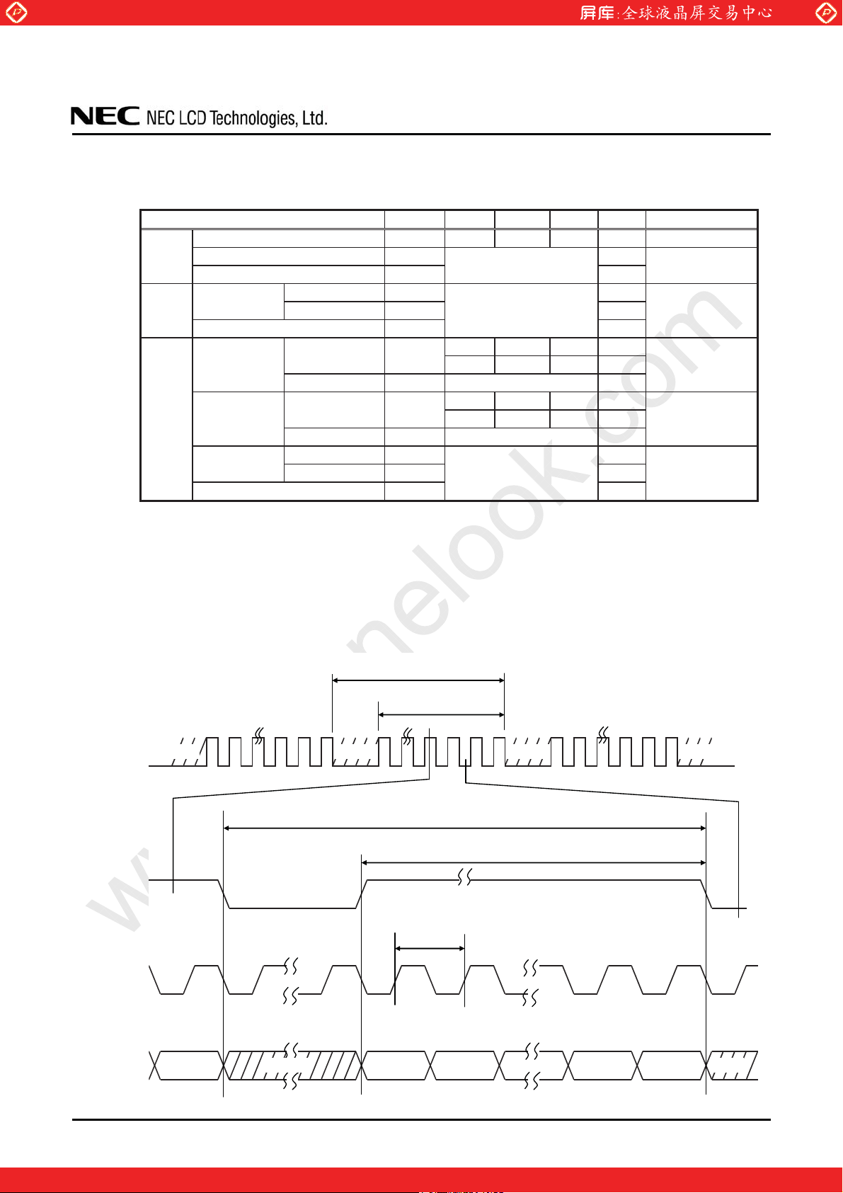
4.9 INPUT SIGNAL TIMINGS
4.9.1 Timing characteristics
Parameter Symbol min. typ. max. Unit Remarks
Frequency 1/tc 80.0 83.26 85.0 MHz 12.01 ns (typ.)
CLK
DATA
DE
CLK-DATA
Horizontal
Vertical
(One frame)
CLK-DE
Duty - -
Rise time, Fall time -
Rise time, Fall time -
Rise time, Fall time -
Note1: Definition of parameters is as follows.
tc = 1CLK, th = 1H
Note2: See the data sheet of LVDS transmitter.
Note3: "th" (CLK number) should be fixed to "16n+k" (n= natural number: 1,2,3, k=0, 2, 4 or 6).
In case "th" is not the specified value, it may cause display deterioration.
e.g.: "th" (CLK number)= 660, 662, 672, 674, 676, 678, 688, 690
www.panelook.com
NL256204AM15-01/01A
-
Setup time - ns
Hold time - ns
Cycle th
Display period thd 640 CLK
Cycle tv
Display period tvd 2,048 H
Setup time - ns
Hold time - ns
7.72 8.071 -
660 672 690 CLK
- 16.667 - ms
2,053 2,064 - H
-
-
ns
ns
Ps
ns
Note2
Note2
123.9 kHz (typ.)
Note1, Note3
60.0 Hz (typ.)
Note1
Note2
4.9.2 Input signal timing chart
DE
DE
CLK
DATA (A) to (D)
Invalid Invalid Invalid Invalid
tv
tvd = 2,048H (fixed)
th
thd = 640CLK (fixed)
tc
DATA SHEET DOD-PD-0887 (4th edition)
One step solution for LCD / PDP / OLED panel application: Datasheet, inventory and accessory!
InvalidInvalid
21
www.panelook.com
Page 22
Global LCD Panel Exchange Center
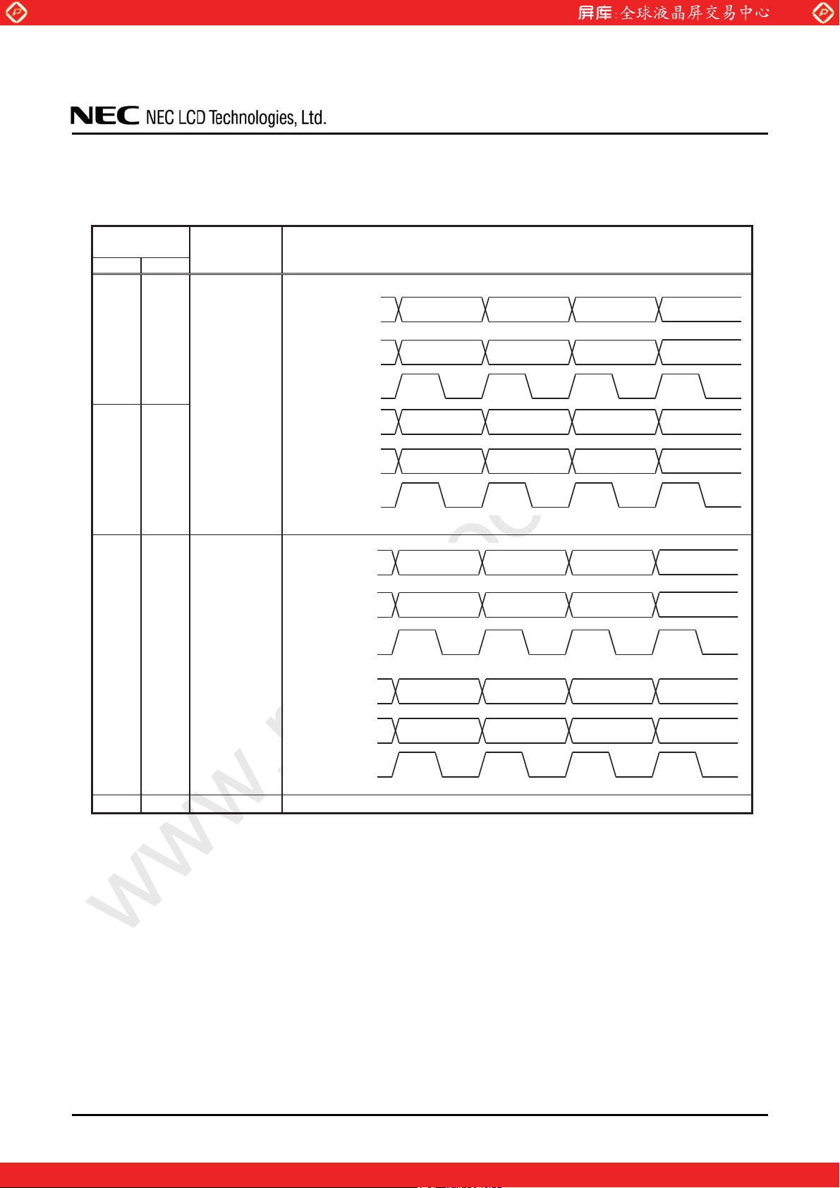
4.10 LVDS DATA TRANSMISSION MODE
Transmission mode of LVDS data is selectable by MOD0 and MOD1 terminal.
www.panelook.com
NL256204AM15-01/01A
MOD>1:0@
Note1
1 0
Open Open
Low Low
Mode name Data transmission chart
Mode 0
L/R
transmission
mode
Mode 1
Pixel Data A
Pixel Data B
Pixel Data C
Pixel Data D
Pixel Data A
Pixel Data B
LA
CA
RA
LB
CB
RB
CLK1
LC
CC
RC
LD
CD
RD
CLK2
LA
CA
RA
LB
CB
RB
CLK1
DO(7:0) D2(7:0) D4(7:0)
D1(7:0) D3(7:0) D5(7:0)
D1280(7:0) D1282(7:0) D1284(7:0)
D1281(7:0) D1283(7:0) D1285(7:0)
DO(7:0) D1(7:0) D2(7:0)
D640(7:0) D641(7:0) D642(7:0)
Open Low
4 divided
transmission
mode
Low Open Reserved
Note1: High must be Open.
Pixel Data C
Pixel Data D
LC
CC
RC
LD
CD
RD
CLK2
D1280(7:0) D1281(7:0) D1282(7:0)
D1920(7:0) D1921(7:0) D1922(7:0)
-
DATA SHEET DOD-PD-0887 (4th edition)
One step solution for LCD / PDP / OLED panel application: Datasheet, inventory and accessory!
22
www.panelook.com
Page 23
Global LCD Panel Exchange Center
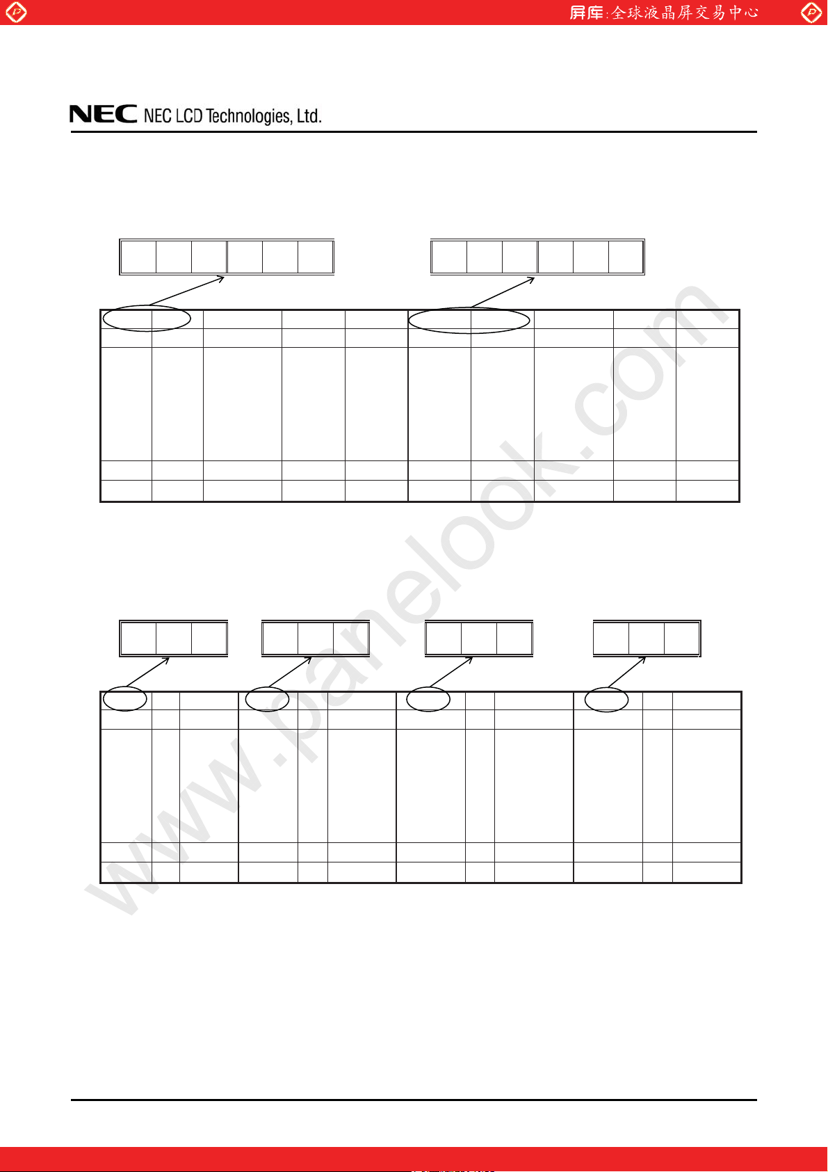
4.11 DISPLAY POSITIONS
(1) Mode0: MOD0= Open, MOD1= Open / MOD0= Low, MOD1= Low
D (0, 0) D (1, 0) D (1280, 0) D (1281, 0)
LA CA RA LB CB RB LC CC RC LD CD RD
www.panelook.com
NL256204AM15-01/01A
0, 0 1, 0
0, 1 1, 1
x
x
x
0, 2046 1, 2046
0, 2047 1, 2047
x
x
x
xxx
xxx
x
x
x
xxx
xxx
1278, 0 1279, 0 1280, 0 1281, 0
1278, 1 1279, 1 1280, 1 1281, 1
x
x
x
1278, 2046 1279, 2046 1280, 2046 1281, 2046
1278, 2047 1279, 2047 1280, 2047 1281, 2047
x
x
x
x
x
x
x
x
x
xxx
xxx
x
x
x
xxx
xxx
(2) Mode1: MOD0= Open, MOD1= Low
D (0, 0) D (640, 0) D (1280, 0) D (1920, 0)
LA CA RA LB CB RB LC CC RC LD CD RD
0, 0
0, 1
639, 0 640, 0
xxx
639, 1 640, 1
xxx
1279, 0 1280, 0
xxx
1279, 1 1280, 1
xxx
xxx
xxx
1919, 0 1920, 0
1919, 1 1920, 1
2558, 0 2559, 0
2558, 1 2559, 1
x
x
x
2558, 2046 2559, 2046
2558, 2047 2559, 2047
xxx
xxx
x
x
x
2559, 0
2559, 1
x
x
x
0, 2046
0, 2047
x
x
x
xxx
xxx
x
x
x
639, 2046 640, 2046
639, 2047 640, 2047
x
x
x
x
x
x
xxx
xxx
DATA SHEET DOD-PD-0887 (4th edition)
x
x
x
1279, 2046 1280, 2046
1279, 2047 1280, 2047
x
x
x
x
x
x
xxx
xxx
x
x
x
1919, 2046 1920, 2046
1919, 2047 1920, 2047
x
x
x
xxx
xxx
One step solution for LCD / PDP / OLED panel application: Datasheet, inventory and accessory!
x
x
x
x
x
x
2559, 2046
2559, 2047
23
www.panelook.com
Page 24
Global LCD Panel Exchange Center
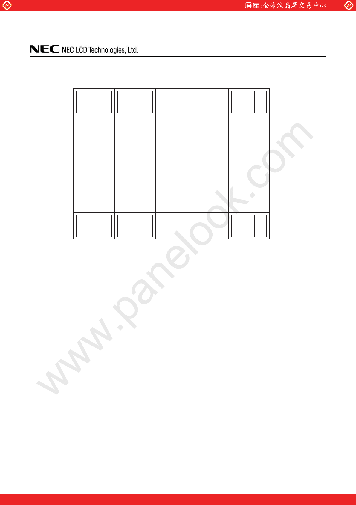
4.12 PIXEL ARRANGNMENT
0 1 2,559
www.panelook.com
NL256204AM15-01/01A
0 L C R L C R
•
•
2,047 L C R L C R • • • • • • • L C R
•
•
•
•
• • • • • • •
• • • • • • •
LCR
•
•
•
DATA SHEET DOD-PD-0887 (4th edition)
One step solution for LCD / PDP / OLED panel application: Datasheet, inventory and accessory!
24
www.panelook.com
Page 25
Global LCD Panel Exchange Center
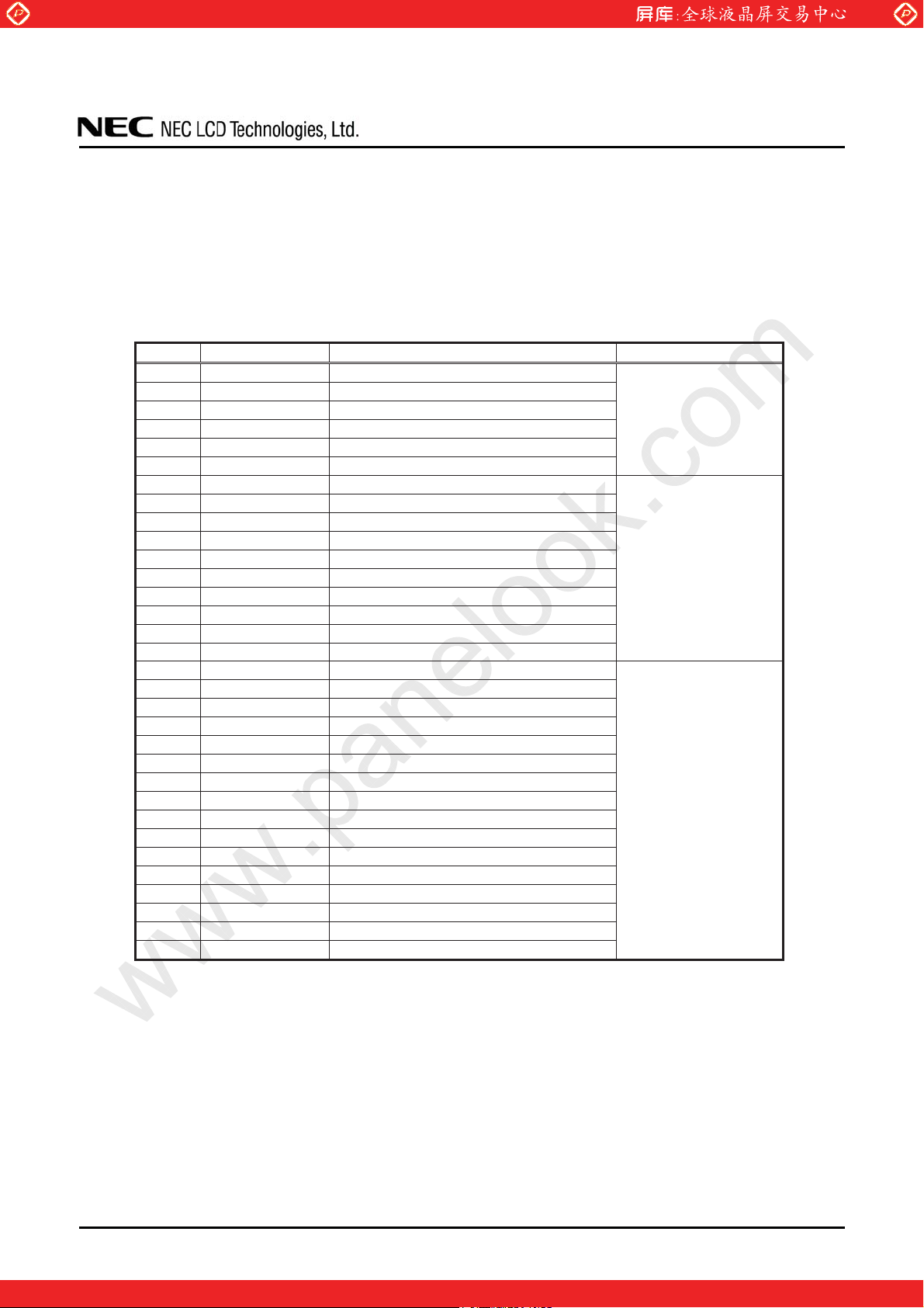
4.13 TEN-bit LOOK UP TABLE FOR GAMMA ADJUSTMENT
Adjustment of gamma characteristics for each 8-bit LCR data is possible by using built-in 10-bit LUT
(look up table) for Gamma characteristics.
The LUT is set with the serial data. The combination of the control command determines
Random/Sequential Address WRITE and Individual/Simultaneous LCR setting.
The serial data is composed as Table1.
Table1: Serial data Composition
DATA DATA name Function Remarks
D31 CMD5 Control Command
D30 CMD4 Control Command
D29 CMD3 Control Command
D28 CMD2 Control Command
D27 CMD1 Control Command
D26 CMD0 Control Command
D25 ADD9 LUT Address (MSB)
D24 ADD8 LUT Address
D23 ADD7 LUT Address
D22 ADD6 LUT Address
D21 ADD5 LUT Address
D20 ADD4 LUT Address
D19 ADD3 LUT Address
D18 ADD2 LUT Address
D17 ADD1 LUT Address
D16 ADD0 LUT Address (LSB)
D15 DATA15 LUT Data (MSB)
D14 DATA14 LUT Data
D13 DATA13 LUT Data
D12 DATA12 LUT Data
D11 DATA11 LUT Data
D10 DATA10 LUT Data
D9 DATA9 LUT Data
D8 DATA8 LUT Data
D7 DATA7 LUT Data
D6 DATA6 LUT Data
D5 DATA5 LUT Data
D4 DATA4 LUT Data
D3 DATA3 LUT Data
D2 DATA2 LUT Data
D1 DATA1 LUT Data
D0 DATA0 LUT Data (LSB)
www.panelook.com
NL256204AM15-01/01A
See Table2 and 3.
See Table4.
See Table5.
DATA SHEET DOD-PD-0887 (4th edition)
One step solution for LCD / PDP / OLED panel application: Datasheet, inventory and accessory!
25
www.panelook.com
Page 26
Global LCD Panel Exchange Center
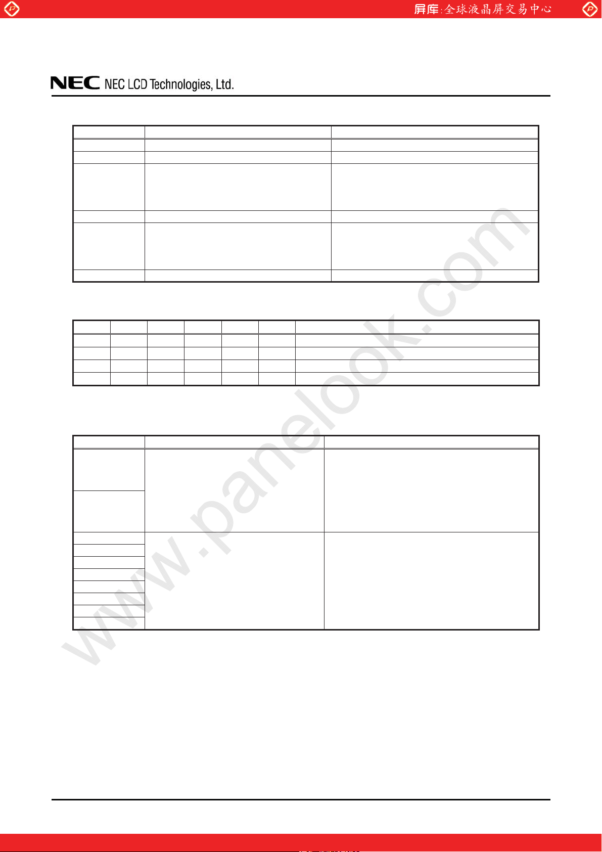
Table2: Command table (CMD5 to CMD0: 6-bit)
DATA name Parameter Remarks
CMD5 Must be set to "1". CMD4 Must be set to "1". -
Selection of Random/Sequential Address
CMD3
CMD2 Must be set to "1". -
CMD1
CMD0 Must be set to "0". -
WRITE
"1": Random Address WRITE
"0": Sequential Address WRITE
Selection of Individual/Simultaneous LCR
setting
"1": Individual LCR setting
"0": Simultaneous LCR setting
www.panelook.com
NL256204AM15-01/01A
-
"1": Select the Sub-pixel by using ADD9 and
ADD8. (See Table4.)
"0": ADD9 and ADD8 are invalid.
Table3: Command table (CMD5 to CMD0: 6-bit)
CMD5 CMD4 CMD3 CMD2 CMD1 CMD0 Function
1 1 1 1 1 0 Random Address WRITE, Individual LCR setting
1 1 1 1 0 0 Random Address WRITE, Simultaneous LCR setting
1 1 0 1 1 0 Sequential Address WRITE, Individual LCR setting
1 1 0 1 0 0 Sequential Address WRITE, Simultaneous LCR setting
*Another combinations are prohibited, and may cause function error.
Table4: Address table (ADD9 to ADD0: 10-bit)
DATA name Parameter Remarks
Sub-pixel Selection
ADD9
ADD8
ADD7
ADD6
ADD5
ADD4
ADD3
ADD2
ADD1
ADD0
ADD>9:8@=
0:0 Left Sub-pixel
0:1 Center Sub-pixel
1:0 Right Sub-pixel
1:1 ON/OFF selection of Gamma
Correction
LUT Address
256 address = 00h - FFh
When "ADD>9:8@=1:1", ON/OFF of Gamma
correction can select according to the GMA>2:0@.
(See Table6 and Table7.)
When "ADD>9:8@ = 1:1",
ADD>7:0@ must be set to 00h.
DATA SHEET DOD-PD-0887 (4th edition)
One step solution for LCD / PDP / OLED panel application: Datasheet, inventory and accessory!
26
www.panelook.com
Page 27
Global LCD Panel Exchange Center
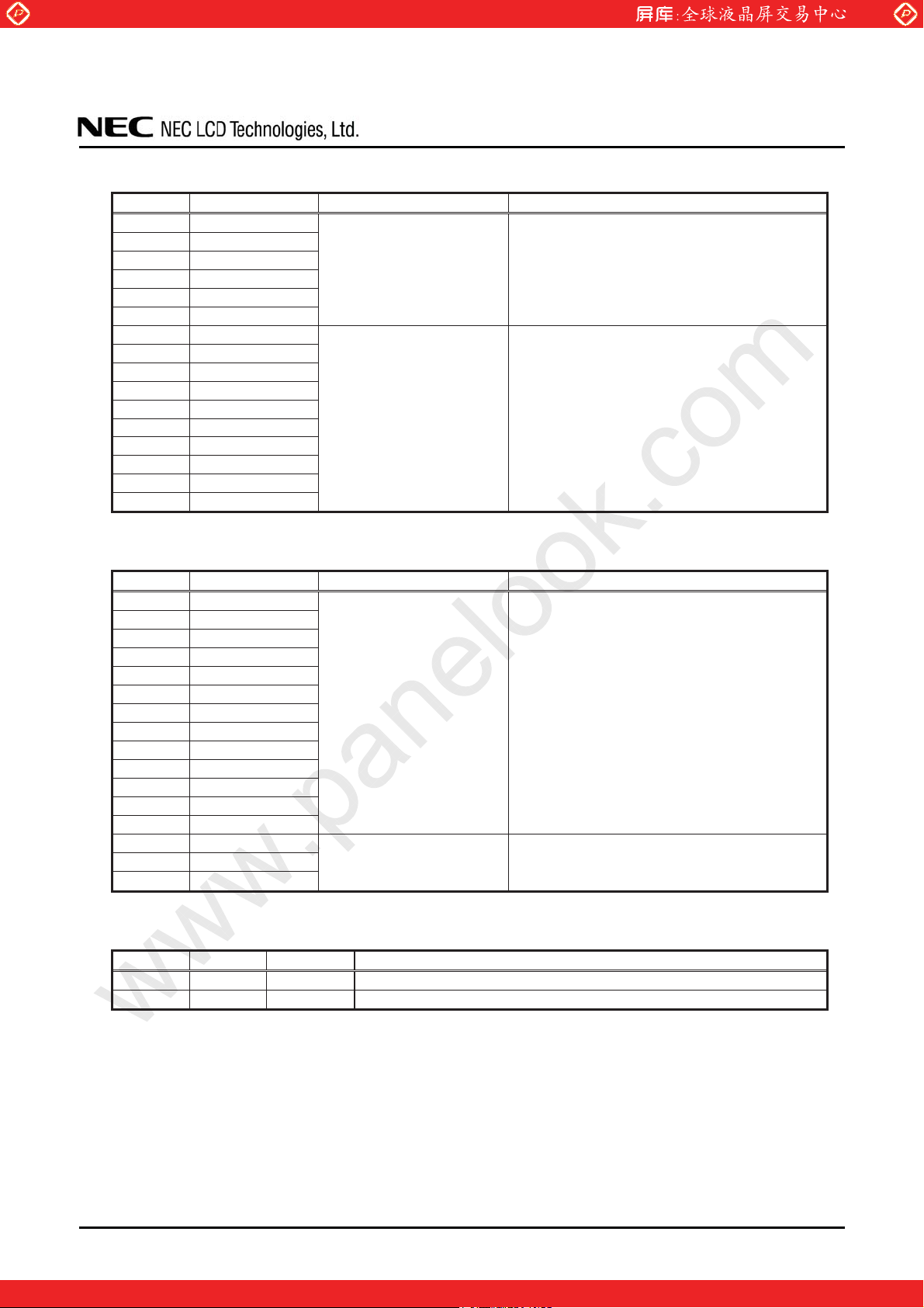
Table5: Data table (DATA15 to DATA0: 16-bit)
DATA DATA name Parameter Remarks
DATA15 Dummy
DATA14 Dummy
DATA13 Dummy
DATA12 Dummy
DATA11 Dummy
DATA10 Dummy
DATA9 DATA9
DATA8 DATA8
DATA7 DATA7
DATA6 DATA6
DATA5 DATA5
DATA4 DATA4
DATA3 DATA3
DATA2 DATA2
DATA1 DATA1
DATA0 DATA0
www.panelook.com
Dummy Data
Must be set to "0".
>MSB@
10-bit LUT Data
000h - 3FFh
>LSB@
NL256204AM15-01/01A
-
-
Table6: Gamma correction table (DATA15 to DATA0: 16-bit)
DATA DATA name Parameter Remarks
DATA15 Dummy
DATA14 Dummy
DATA13 Dummy
DATA12 Dummy
DATA11 Dummy
DATA10 Dummy
DATA9 Dummy
DATA8 Dummy
DATA7 Dummy
DATA6 Dummy
DATA5 Dummy
DATA4 Dummy
DATA3 Dummy
DATA2 GAM2
DATA1 GAM1
DATA0 GAM0
Table7: Control code GAM
GMA2 GMA1 GMA0 Function
0 0 0 No correction (Initial setting)
0 0 1 Correction according to the LUT Data. Note1
Dummy Data
Must be set to "0".
>MSB@
GMA Data
>LSB@
>2:0@
-
See Table7.
*Another combinations are prohibited, and may cause function error.
Note1: Initial setting of the LUT is undefined data. The LUT should be enabled by setting of the GMA after
writing the LUT data in all the 256 addresses, in order to avoid undefined data display.
Note2: Transfer the data every power-on, because the LUT data isn't stored in the LCD module.
Note3: When writing and reading the LUT data, a noise may appear on the display image. In order to
prevent the noise appearing on the display, following measures should be performed.
(1)The LUT data should be rewritten during invalid period of pixel data (See "4.8 INPUT
SIGNAL TIMINGS".).
(2)The LUT data should be rewritten while the LUT data is invalid.
DATA SHEET DOD-PD-0887 (4th edition)
One step solution for LCD / PDP / OLED panel application: Datasheet, inventory and accessory!
ყ
27
www.panelook.com
Page 28
Global LCD Panel Exchange Center
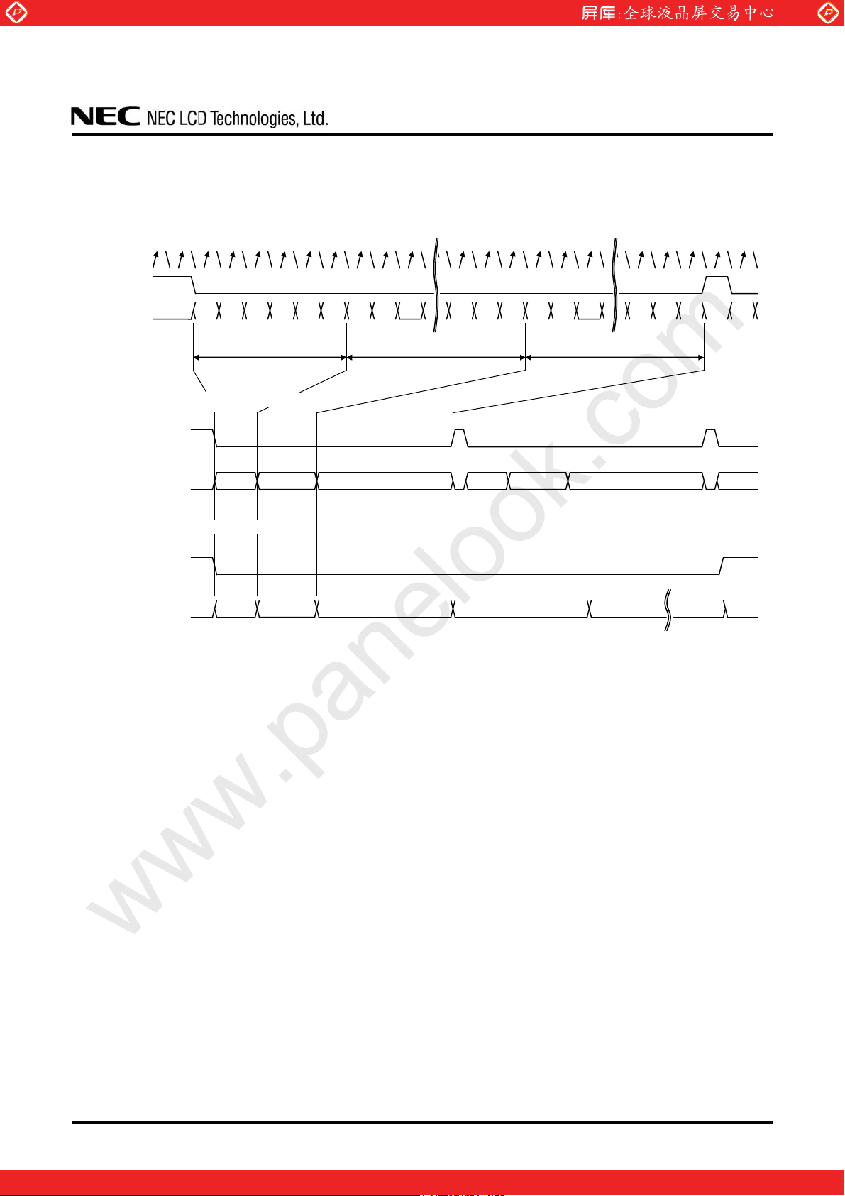
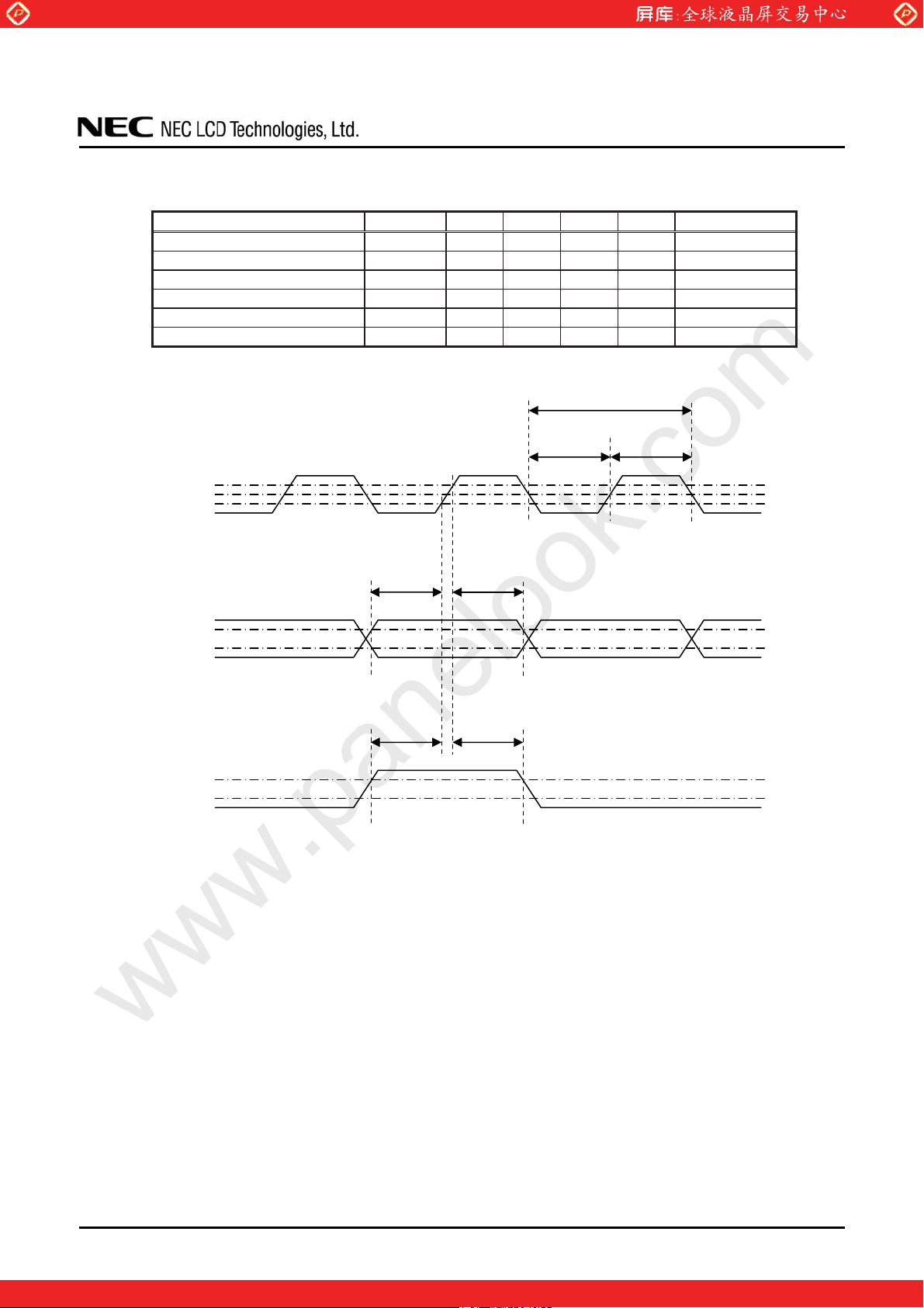
4.14 LUT SERIAL COMMUNICATION TIMINGS
(1) Timing chart
SCLK
CSR, CSL
D31 D30 D29 D28 D27 D26 D25 D24 D23 D18 D17 D16 D15 D14 D13 D2 D1 D0
SDAT
Invalid
www.panelook.com
NL256204AM15-01/01A
Invalid
D31
Random Address WRITE timing chart
CSR, CSL
CMD ADD DATA CMD ADD DATA
SDAT
Invalid
Sequential Address WRITE timing chart
CSR, CSL
CMD ADD DATA DATA
SDAT
Invalid
ADD[9:0]
DATA[15:0] CMD[5:0]
Invalid Invalid
DATA
Invalid
DATA SHEET DOD-PD-0887 (4th edition)
One step solution for LCD / PDP / OLED panel application: Datasheet, inventory and accessory!
28
www.panelook.com
Page 29
Global LCD Panel Exchange Center
(2) Timing specifications
Parameter Symbol min. typ. max. Unit Remarks
SCLK Frequency 1/Tsck - - 5 MHz SCLK Pulse Twsck 50 - - ns SDAT-SCLK Setup Time Tds 50 - - ns SDAT-SCLK Hold Time Tdh 50 - - ns CSR/CSL-SCLK Setup Time Tcs 50 - - ns CSR/CSL-SCLK Hold Time Tch 50 - - ns -
www.panelook.com
NL256204AM15-01/01A
Tsck
Twsck Twsc k
V+
SCLK
Tds Tdh
SDATI
Tcs
CSR,
CSL
Note1: During the serial communication mode, the display noise may appear because of rewriting the
data. To avoid this, rewrite the data in the blanking timing. The external noise may cause the
data change, refresh the data regularly according to need.
Tch
50%
V-
V+
V-
V+
V-
DATA SHEET DOD-PD-0887 (4th edition)
One step solution for LCD / PDP / OLED panel application: Datasheet, inventory and accessory!
29
www.panelook.com
Page 30
Global LCD Panel Exchange Center
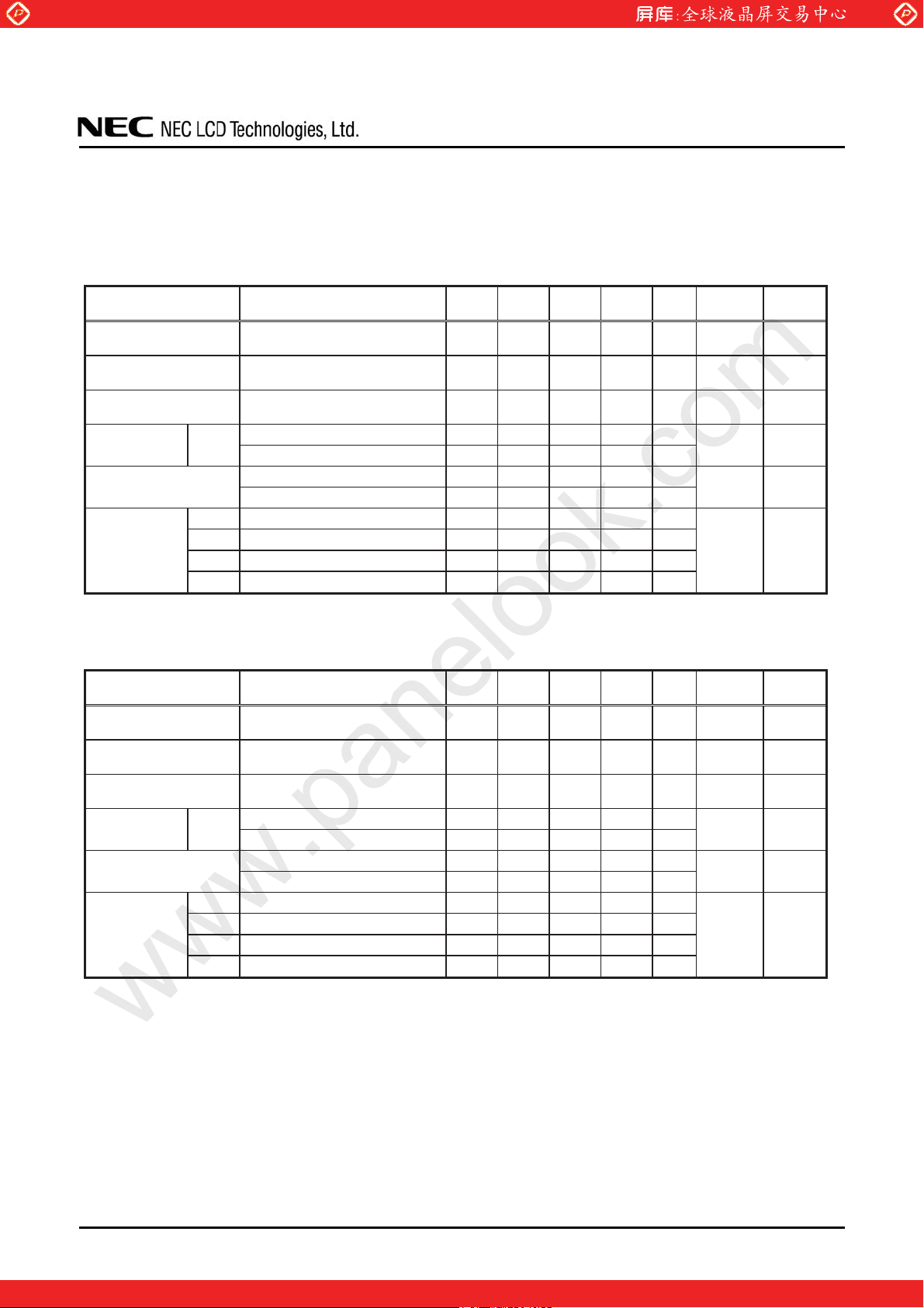
4.15 OPTICS
4.15.1 Optical characteristics
(1) NL256204AM15-01
Parameter Condition Symbol min. typ. max. Unit
Luminance
Contrast ratio
Luminance uniformity
Chromaticity White
Response time
Right
Viewing angle
Left
Up
Down
TR
TR
TR
White at center
= 0q, TL= 0q,TU= 0q, TD= 0q
White/Black at center
= 0q, TL= 0q,TU= 0q, TD= 0q
= 0q, TL= 0q,TU= 0q, TD= 0q
Black to White Ton - 15 25 ms
White to Black Toff - 15 25 ms
TU = 0q, TD = 0q, CR t 10 TR
TU = 0q, TD = 0q, CR t 10 TL
TR = 0q, TL = 0q, CR t 10 TU
TR = 0q, TL = 0q, CR t 10 TD
www.panelook.com
L 650 850 - cd/m
CR 400 600 - -
White
x coordinate Wx
y coordinate Wy
LU - 1.1 1.3 - BM-5A Note4
NL256204AM15-01/01A
0.255 - -
-
0.310 - -
-
70 85 -
70 85 -
70 85 -
70 85 -
Measuring
instrument
BM-5A
2
or SR-3
BM-5A
or SR-3
SR-3 Note5
BM-5A
q
q
BM-5A Note8
q
q
(Note1, Note2)
Remarks
-
Note3
Note6
Note7
(2) NL256204AM15-01A
Parameter Condition Symbol min. typ. max. Unit
Luminance
Contrast ratio
Luminance uniformity
Chromaticity White
Response time
Right
Viewing angle
Left
Up
Down
White at center
= 0q, TL= 0q,TU= 0q, TD= 0q
TR
White/Black at center
= 0q, TL= 0q,TU= 0q, TD= 0q
TR
White
= 0q, TL= 0q,TU= 0q, TD= 0q
TR
x coordinate Wx
y coordinate Wy
Black to White Ton - 15 25 ms
White to Black Toff - 15 25 ms
TU = 0q, TD = 0q, CR t 10 TR
TU = 0q, TD = 0q, CR t 10 TL
TR = 0q, TL = 0q, CR t 10 TU
TR = 0q, TL = 0q, CR t 10 TD
L 650 850 - cd/m
CR 400 600 - -
LU - 1.1 1.3 - BM-5A Note4
0.280 - -
-
0.304 - -
-
70 85 -
70 85 -
70 85 -
70 85 -
Measuring
instrument
BM-5A
2
or SR-3
BM-5A
or SR-3
SR-3 Note5
BM-5A
q
q
BM-5A Note8
q
q
(Note1, Note2)
Remarks
-
Note3
Note6
Note7
DATA SHEET DOD-PD-0887 (4th edition)
One step solution for LCD / PDP / OLED panel application: Datasheet, inventory and accessory!
30
www.panelook.com
Page 31
Global LCD Panel Exchange Center
Note1: These are initial characteristics.
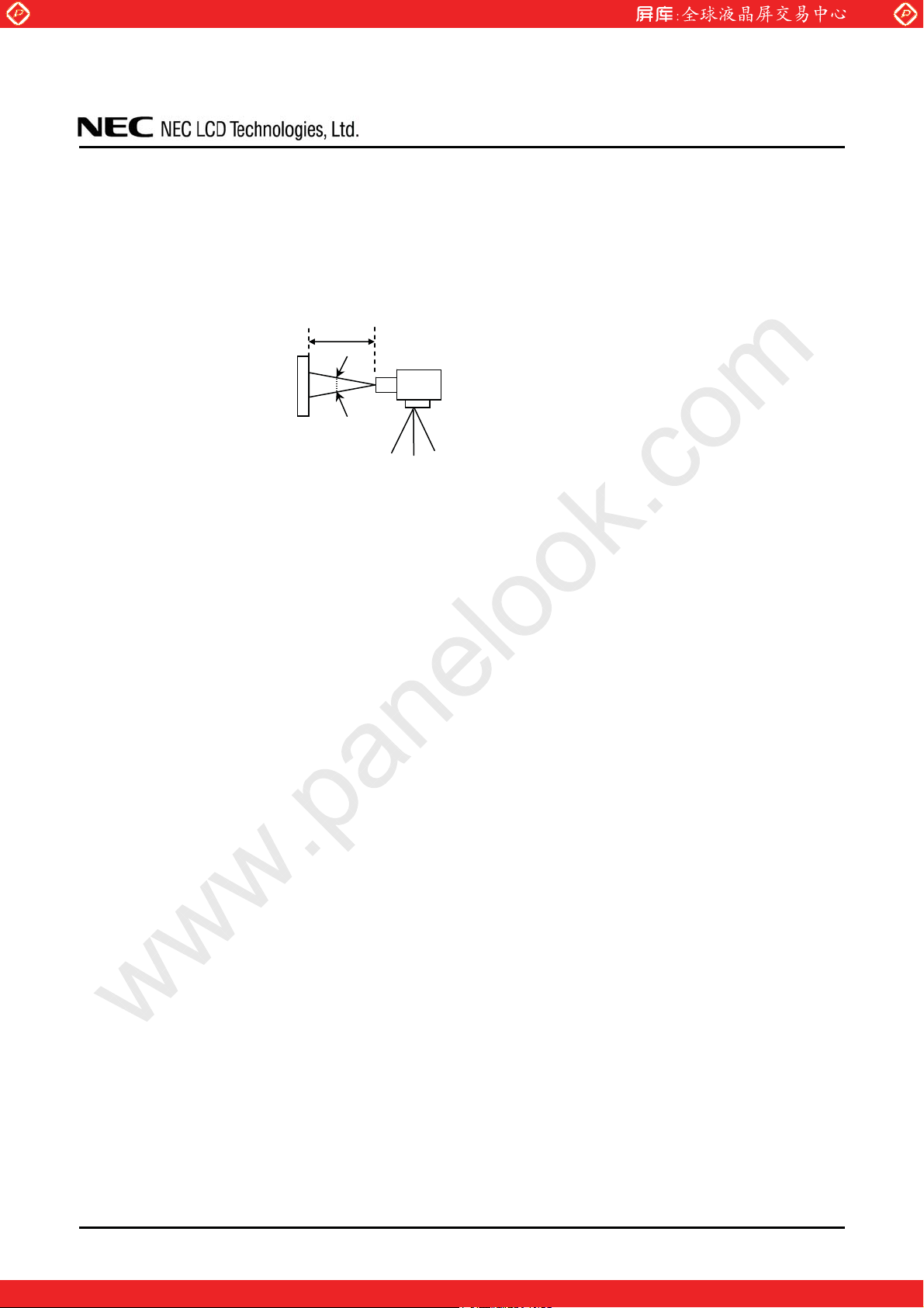
Note2: Measurement conditions are as follows.
qC, VDD=12V, VDDB=12V, Luminance control = maximum, Display mode: QSXGA,
Ta=25
Horizontal cycle=1/123.9 kHz, Vertical cycle = 1/60.0 Hz
Optical characteristics are measured after 20minutes from working the product, in the dark
room. Also measurement method for luminance is as follows.
www.panelook.com
NL256204AM15-01/01A
50cm
Photodetector (TOPCON BM-5A, SR-3)
LCD module
(Product)
1q
Note3: See "4.15.2 Definition of contrast ratio".
Note4: See "4.15.3 Definition of luminance uniformity".
Note5: These coordinates are found on CIE 1931 chromaticity diagram.
Note6: Product surface temperature: TopF=36qC
Note7: See "4.15.4 Definition of response times".
Note8: See "4.15.5 Definition of viewing angles".
DATA SHEET DOD-PD-0887 (4th edition)
One step solution for LCD / PDP / OLED panel application: Datasheet, inventory and accessory!
31
www.panelook.com
Page 32
Global LCD Panel Exchange Center
ུ
ུ
ི
ཱི
ུ
ཱ
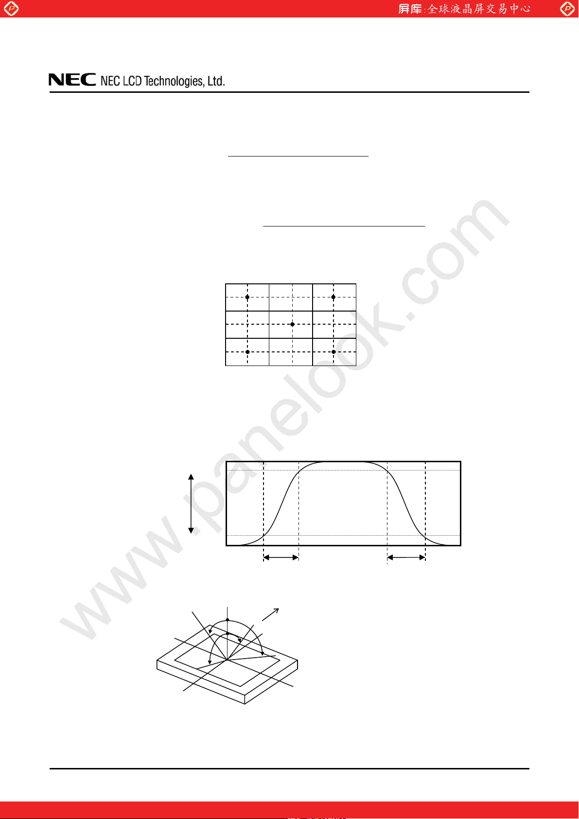
4.15.2 Definition of contrast ratio
The contrast ratio is calculated by using the following formula.
Contrast ratio (CR) =
4.15.3 Definition of luminance uniformity
The luminance uniformity is calculated by using following formula.
Luminance uniformity (LU) =
The luminance is measured at near the 5 points shown below.
www.panelook.com
Luminance of white screen
Luminance of black screen
Maximum luminance from to
Minimum luminance from to
NL256204AM15-01/01A
341
1,023
1,706
427
1,279
2,132
4.15.4 Definition of response times
Response time is measured, the luminance changes from "black" to "white", or "white" to "black" on
the same screen point, by photo-detector. Ton is the time it takes the luminance change from 10% up
to 90%. Also Toff is the time it takes the luminance change from 90% down to 10% (See the
following diagram.).
100%
White
Luminance
Black
90%
10%
0%
Ton
Tof f
4.15.5 Definition of viewing angles
Normal axis (Perpendicular)
12 o’clock
TL
Left
TU
Upper
TR
TD
Lower
DATA SHEET DOD-PD-0887 (4th edition)
One step solution for LCD / PDP / OLED panel application: Datasheet, inventory and accessory!
Right
32
www.panelook.com
Page 33
Global LCD Panel Exchange Center
5. RELIABILITY TESTS
Test item Condition Judgment Note1
www.panelook.com
NL256204AM15-01/01A
High temperature and humidity
(Operation)
Heat cycle
(Operation)
Thermal shock
(Non operation)
Vibration
(Non operation)
Mechanical shock
(Non operation)
ESD
(Operation)
Dust
(Operation)
Non-operation
Low pressure
Operation
60 r 2qC, RH = 60%, 240hours
ཱ Display data is white.
0 r 3qC}1hour
55 r 3qC}1hour
ཱ 50cycles, 4hours/cycle
ི Display data is white.
-20 r 3qC}30minutes
60 r 3qC}30minutes
ཱ 100cycles, 1hour/cycle
ི Temperature transition time is within 5
minutes.
5 to 100Hz, 11.76m/s
ཱ 1 minute/cycle
ི X, Y, Z direction
ཱི 10 times each directions
294m/ s
ཱ X, Y, Z direction
ི 3 times each directions
150pF, 150:, r10kV
ཱ 9 places on a panel surface Note2
ི 10 times each places at 1 sec interval
Sample dust: No.15 (by JIS-Z8901)
ཱ 15 seconds stir
ི 8 times repeat at 1 hour interval
15 kPa (Equivalent to altitude 13,600m)
ཱ -20qCr3qC}24 hours
ི +60qCr3qC}24 hours
53.3 kPa (Equivalent to altitude 4,850m)
ཱ 0qCr3qC}24 hours
ི +55qCr3qC}24 hours
2
, 11ms
2
No display malfunctions
No display malfunctions
No physical damages
No display malfunctions
No display malfunctions
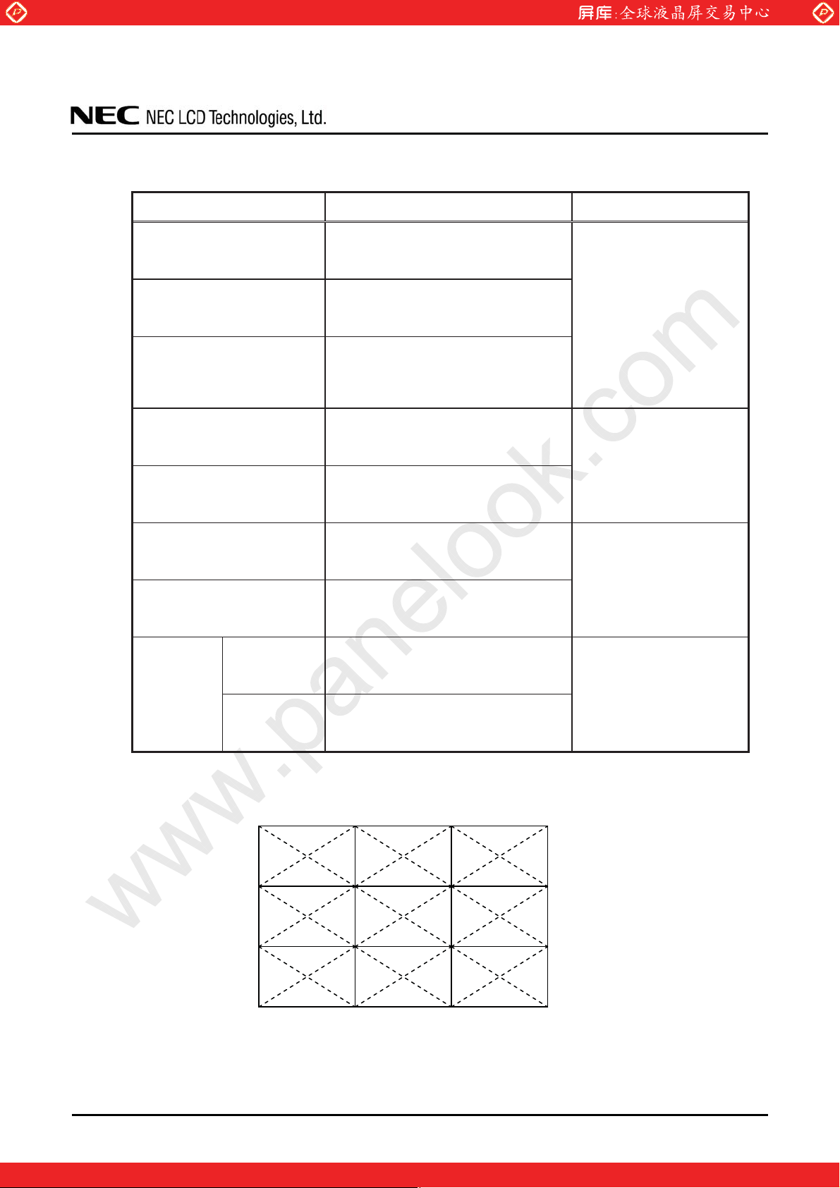
Note1: Display and appearance are checked under environmental conditions equivalent to the
inspection conditions of defect criteria.
Note2: See the following figure for discharge points
{
{
{
DATA SHEET DOD-PD-0887 (4th edition)
{
{
{
{
{
{
33
One step solution for LCD / PDP / OLED panel application: Datasheet, inventory and accessory!
www.panelook.com
Page 34
Global LCD Panel Exchange Center
!
6. PRECAUTIONS
6.1 MEANING OF CAUTION SIGNS
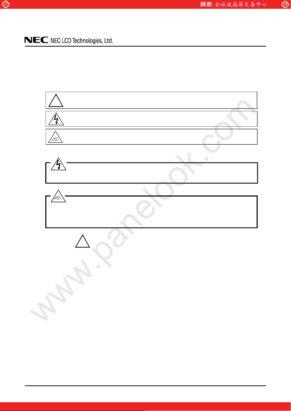
The following caution signs have very important meaning. Be sure to read "6.2 CAUTIONS" and
"6.3 ATTENTIONS", after understanding these contents!
This sign has the meaning that customer will be injured by himself or the product will
sustain a damage, if customer has wrong operations.
This sign has the meaning that customer will get an electrical shock, if customer has
wrong operations.
This sign has the meaning that customer will be injured by himself, if customer has
wrong operations.
www.panelook.com
NL256204AM15-01/01A
6.2 CAUTIONS
Do not touch the working backlight. Customer will be in danger of an electric shock.
Do not touch the working backlight. Customer will be in danger of burn injury.
Do not shock and press the LCD panel and the backlight! There is a danger of breaking,
because they are made of glass. (Shock: To be not greater 294m/s
11ms, Pressure: To be not greater 19.6N)
6.3 ATTENTIONS
6.3.1 Handling of the product
Take hold of both ends without touch the circuit board when customer pulls out products (LCD
modules) from inner packing box. If customer touches it, products may be broken down or out of
adjustment, because of stress to mounting parts.
ཱ Do not hook nor pull cables such as lamp cable, and so on, in order to avoid damage.
ི If customer puts down the product temporarily, the product puts on flat subsoil as a display side turns
down.
ཱི Take the measures of electrostatic discharge with such as earth band, ionic shower and so on, because
products may be damaged by electrostatic when customer handles the product.
ུ The torque for product mounting screws must never exceed 0.45 Nm. Higher torque values might
result in distortion of the bezel.
!
2
and to be not greater
DATA SHEET DOD-PD-0887 (4th edition)
One step solution for LCD / PDP / OLED panel application: Datasheet, inventory and accessory!
34
www.panelook.com
Page 35
Global LCD Panel Exchange Center
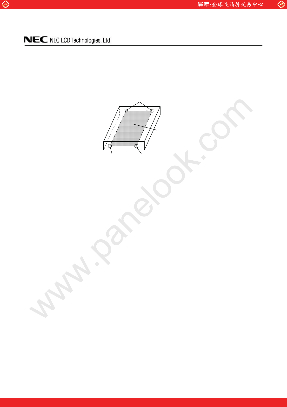
ཱུ The product must be installed using mounting holes without undue stress such as bends or twist (See
outline drawings). And do not add undue stress to any portion (such as bezel flat area) except
mounting hole portion.
Bends or twist described above and undue stress to any portion except mounting hole portion may
cause display un-uniformity.
Recommendation installing method: An ideal plane that is defined by datum point and mounting holes
is to be flush within r0.3 mm.
Product
ྲྀ Do not press or rub on the sensitive display surface. If customer clean on the panel surface, NEC
recommends using the cloth with ethanolic liquid such as screen cleaner for LCD.
ཷ Do not push nor pull the interface connectors while the product is working.
ླྀ When not connecting FG of the LCD module to the customer's equipment ground, inverter noise may
create a beat frequency that will cause video noise on the LCD screen.
ཹ When customer handles the product, use of an original protection sheet on the product surface
(polarizer) is recommended for protection of product surface. Adhesive type protection sheet may
change color or properties of the polarizer.
Datum point
www.panelook.com
NL256204AM15-01/01A
Mounting hole
An ideal plane defined by datum
point and mounting holes
Mounting hole
6.3.2 Environment
Do not operate or store in high temperature, high humidity, dewdrop atmosphere or corrosive gases.
Keep the product in packing box and antistatic pouch in room temperature to avoid for dusts and
sunlight, when customer stores the product.
ཱ In order to prevent dew condensation occurring by temperature difference, the product packing box
should be opened after being left under the environment of an unpacking room enough. Because a
situation of dew condensation occurring is changed by the environmental temperature and humidity.
Evaluate the leaving time sufficiently. (Recommendation leaving time: 6 hour or more with packing
state)
ི Do not operate in high magnetic field. Circuit boards may be broken down by it.
ཱི This product is not designed as radiation hardened.
DATA SHEET DOD-PD-0887 (4th edition)
One step solution for LCD / PDP / OLED panel application: Datasheet, inventory and accessory!
35
www.panelook.com
Page 36
Global LCD Panel Exchange Center
6.3.3 Characteristics
The following items are neither defects nor failures.
Response time, luminance and color may be changed by ambient temperature.
ཱ The LCD may be seemed luminance non-uniformity, flicker, vertical seam or small spot by display
patterns.
ི Optical characteristics (e.g. luminance, display uniformity, etc.) gradually is going to change
depending on operating time, and especially low temperature, because the LCD has cold cathode
fluorescent lamps.
ཱི Do not display the fixed pattern for a long time because it may cause image sticking. Use a screen
saver, if the fixed pattern is displayed on the screen.
ུ The display color may be changed by viewing angle because of the use of condenser sheet in the
backlight.
ཱུ Optical characteristics may be changed by input signal timings.
ྲྀ The interference noise of input signal frequency for this product's signal processing board and
luminance control frequency of inverter may appear on a display. Set up luminance control frequency
of inverter so that the interference noise does not appear.
www.panelook.com
NL256204AM15-01/01A
6.3.4 Other
All VCC and GND terminals should be used without any non-connected lines.
ཱ Do not disassemble a product or adjust variable resistors without permission of NEC.
ི See "REPLACEMENT MANUAL FOR BACKLIGHT UNIT", if customer would like to replace
backlight lamps.
ཱི Pay attention not to insert waste materials inside of products, if customer uses screwnails.
ུ Pack the product with original shipping package, in order to avoid any damages during transportation,
when customer returns it to NEC for repair and so on.
ཱུ The LCD module by itself or integrated into end product should be packed and transported with
display in the vertically position. Otherwise the display characteristics may be impaired.
DATA SHEET DOD-PD-0887 (4th edition)
One step solution for LCD / PDP / OLED panel application: Datasheet, inventory and accessory!
36
www.panelook.com
Page 37
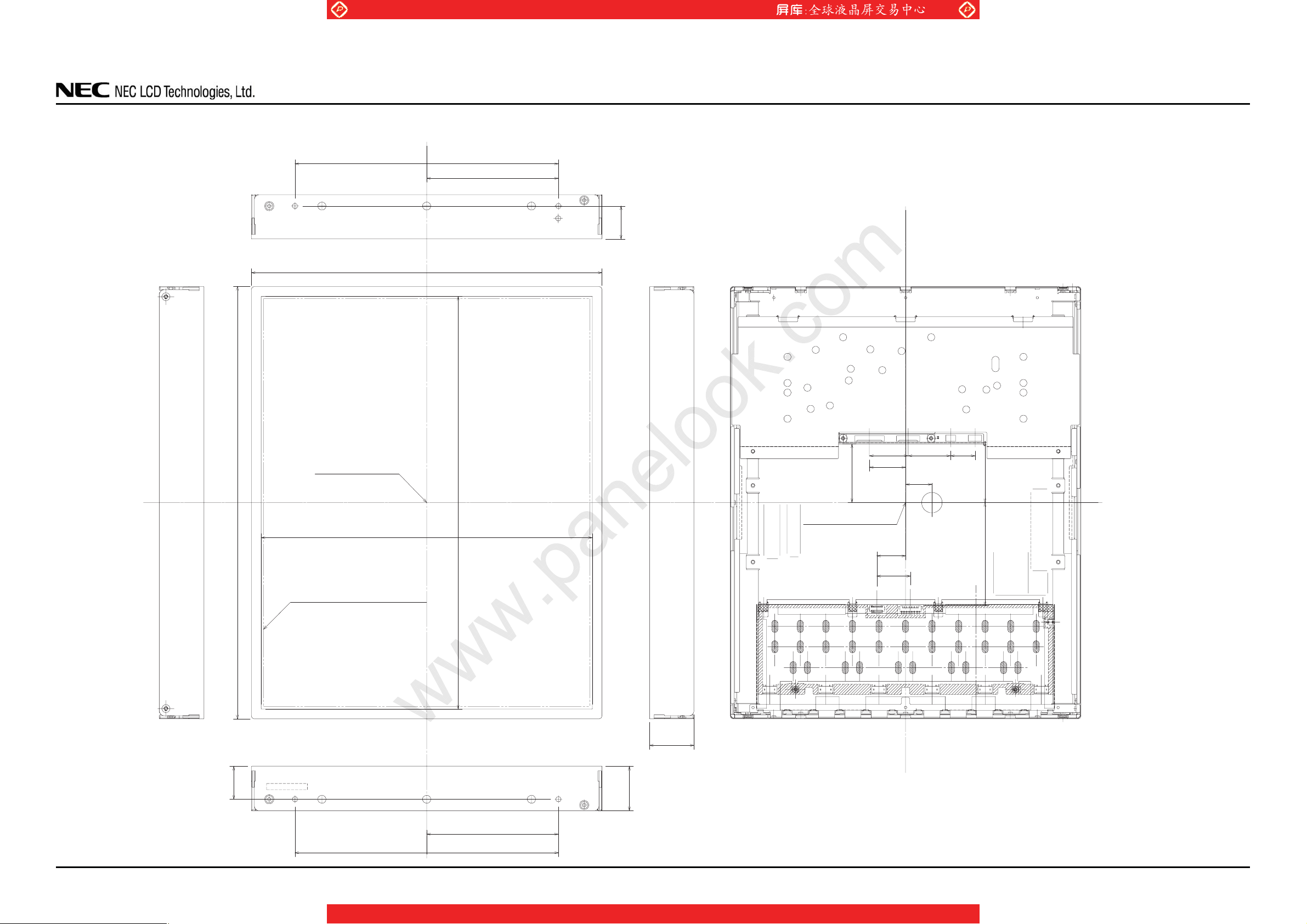
7. OUTLINE DRAWINGS
Global LCD Panel Exchange Center
᧤᧥
www.panelook.com
NL256204AM15-01/01A
%(=(/ 23(1 ,1* $5($
',63/$< $5($ &(17(5
352'8&7 &(1 7(5
' ,63/$< $5($
%(=(/ 23(1 ,1* $5($
' ,63 /$< $5($ &(17(5
᧤ ᧥
᧤ ᧥
&1 &1
&1
᧤ ᧥
᧤ ᧥
&1
&1&1
᧤᧥
0D WH U LD O ,QIR UPD W LRQ
᧤ ᧥
'LIIXVHU! 3&
Note1: The dimensions in parenthesis are for reference.
Note2: Not shown tolerances of the dimensions
0 mm < d 18mm: ±0.2mm.
18 mm < d 50mm: ±0.3mm.
50 mm < d 120mm: ±0.4mm.
120 mm < d 250mm: ±0.5mm.
250 mm < d : ±0.6mm.
᧤᧥
(d: dimension)
Unit: mm
DATA SHEET DOD-PD-0887 (4th edition)
One step solution for LCD / PDP / OLED panel application: Datasheet, inventory and accessory!
37
www.panelook.com
 Loading...