

Page 1
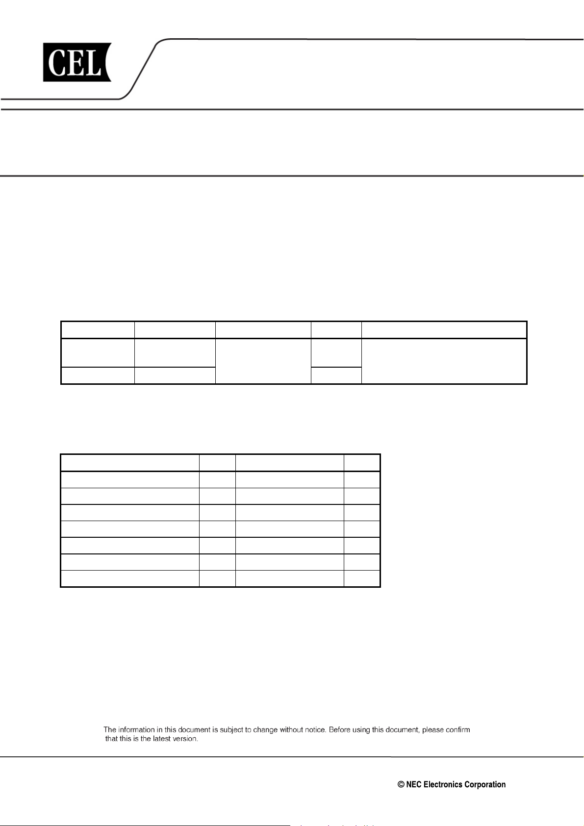
NPN SILICON GERMANIUM C RF TRANSISTOR
NESG4030M14
NPN SiGe:C RF TRANSISTOR FOR
LOW NOISE, HIGH-GAIN AMPLIFICATION
4-PIN LEAD-LESS MINIMOLD (M14, 1208 PKG)
FEATURES
• The device is an ideal choice for low noise, high-gain amplification
NF = 1.1 dB TYP., G
• Maximum stable power gain: MSG = 15 dB TYP. @ V
• SiGe:C HBT technology (UHS4) adopted
• Improvement of ESD protection
• 4-pin lead-less minimold (M14, 1208 PKG)
ORDERING INFORMATION
Part Number Order Number Package Quantity Supplying Form
a = 11.5 dB TYP. @ VCE = 2 V, IC = 6 mA, f = 5.8 GHz
CE = 2 V, IC = 20 mA, f = 5.8 GHz
NESG4030M14 NESG4030M14-A 4-pin lead-less minimold
(M14, 1208 PKG)
NESG4030M14-T3 NESG4030M14-T3-A 10 kpcs/reel
(Pb-Free)
50 pcs
(Non reel)
• 8 mm wide embossed taping
• Pin 1 (Collector), Pin 4 (Emitter) face the
perforation side of the tape
Remark To order evaluation samples, please contact your nearby sales office.
Unit sample quantity is 50 pcs.
ABSOLUTE MAXIMUM RATINGS (TA = +25°C)
Parameter Symbol Ratings Unit
Collector to Base Voltage VCBO
Collector to Emitter Voltage VCEO 3.0 V
Base Current IB
Collector Current IC 35 mA
Total Power Dissipation Ptot
Junction Temperature Tj 150 °C
Storage Temperature Tstg −65 to +150 °C
Note 1
5.0 V
Note 1
12 mA
Note 2
105 mW
Notes 1. VCBO and IB are limited by the permissible current of the protection element.
2. Mounted on 1.08 cm
2
× 1.0 mm (t) glass epoxy PWB
Caution Observe precautions when handling because these devices are sensitive to electrostatic discharge.
Document No. PU10728EJ02V0DS (2nd edition)
Date Published August 2009 NS
The revised points can be easily searched by copying an "<R>" in the PDF file and specifying it in the "Find what:" field.
The mark <R> shows major revised points.
2008, 2009
Page 2
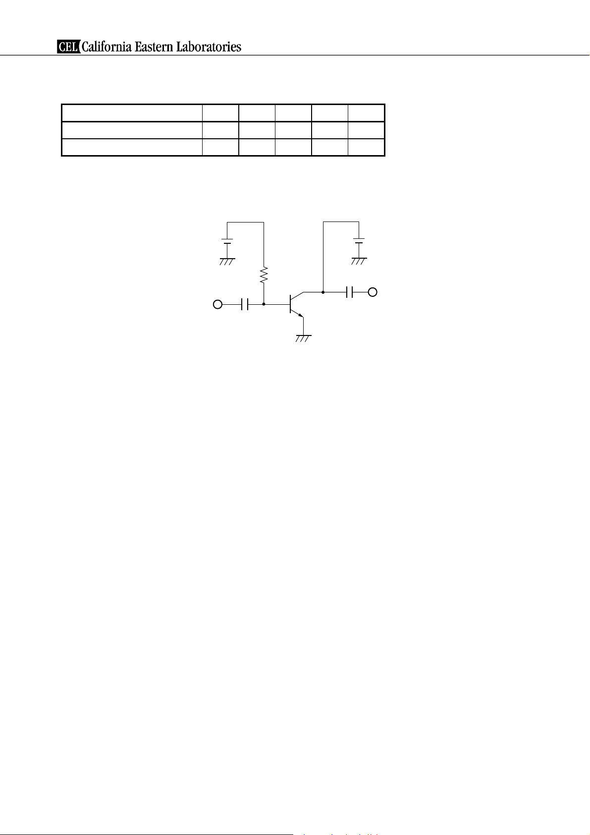
RECOMMENDED OPERATING RANGE (TA = +25°C)
Parameter Symbol MIN. TYP. MAX. Unit
NESG4030M14
Input Power Pin
Base Feedback Resister Rb
− −
− −
3 dBm
150 kΩ
Remark When the voltage return bias circuit like the figure below is used, a current increase is seen because the
ESD protection element is turned on when recommended range of motion in the above table is exceeded.
However, there is no influence of reliability, including deterioration.
R
b
2
Data Sheet PU10728EJ02V0DS
Page 3
<R>
NESG4030M14
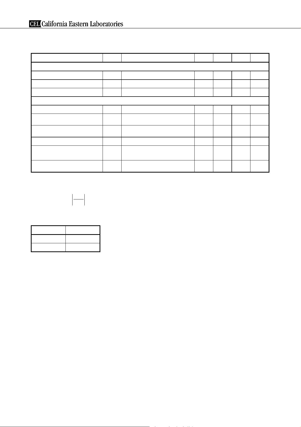
ELECTRICAL CHARACTERISTICS (TA = +25°C)
Parameter Symbol Test Conditions MIN. TYP. MAX. Unit
DC Characteristics
Collector Cut-off Current ICBO VCB = 4.3 V, IE = 0 mA
Emitter Cut-off Current IEBO VEB = 0.4 V, IC = 0 mA
DC Current Gain hFE
Note 1
VCE = 2 V, IC = 6 mA 270 400 540
− −
− −
RF Characteristics
Insertion Power Gain ⏐S21e⏐2 VCE = 2 V, IC = 20 mA, f = 5.8 GHz 8.5 10.5
Noise Figure NF
Associated Gain Ga
Reverse Transfer Capacitance Cre
Maximum Stable Power Gain MSG
Note 2
Note
3
Gain 1 dB Compression Output Power PO (1 dB)
V
Z
S = ZSopt, ZL = ZLopt
CE = 2 V, IC = 6 mA, f = 5.8 GHz,
V
Z
S = ZSopt, ZL = ZLopt
VCB = 2 V, IE = 0 mA, f = 1 MHz
V
CE = 2 V, IC = 20 mA, f = 5.8 GHz 13 15
CE = 2 V, IC (set) = 6 mA,
V
f = 5.8 GHz, Z
S = ZSopt, ZL = ZLopt
−
9.5 11.5
−
−
1.1 1.5 dB
0.12 0.25 pF
9
CE = 2 V, IC = 6 mA, f = 5.8 GHz,
μ
Notes 1. Pulse measurement: PW ≤ 350
s, Duty Cycle ≤ 2%
2. Collector to base capacitance when the emitter grounded
S
3. MSG =
21
S
12
hFE CLASSIFICATION
Rank FB/YFB
Marking zK
hFE Value 270 to 540
100 nA
100 nA
−
−
−
−
−
dB
dB
dB
dBm
Data Sheet PU10728EJ02V0DS
3
Page 4
NESG4030M14
<R>
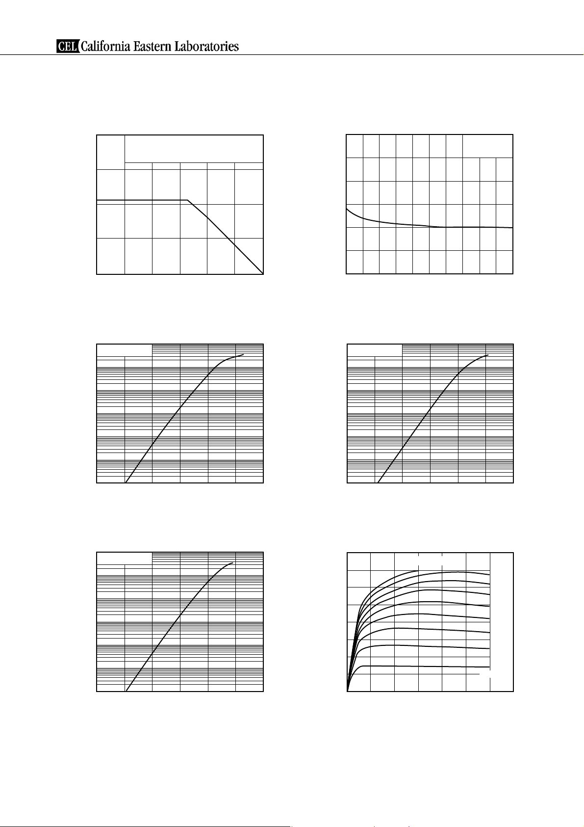
TYPICAL CHARACTERISTICS (TA = +25°C, unless otherwise specified)
TOTAL POWER DISSIPATION
vs. AMBIENT TEMPERATURE
200
Mounted on Glass Epoxy PWB
(1.08 cm
(mW)
tot
150
100
50
Total Power Dissipation P
0
25 50 75 100 125 150
Ambient Temperature TA (°C)
COLLECTOR CURRENT vs.
BASE TO EMITTER VOLTAGE
100
VCE = 1 V
10
2
× 1.0 mm (t) )
REVERSE TRANSFER CAPACITANCE
vs. COLLECTOR TO BASE VOLTAGE
0.3
(pF)
re
0.2
0.1
Reverse Transfer Capacitance C
02468
Collector to Base Voltage VCB (V)
COLLECTOR CURRENT vs.
BASE TO EMITTER VOLTAGE
100
VCE = 2 V
10
f = 1 MHz
10
(mA)
C
1
0.1
0.01
Collector Current I
0.001
0.0001
Base to Emitter Voltage VBE (V)
COLLECTOR CURRENT vs.
BASE TO EMITTER VOLTAGE
100
VCE = 3 V
10
(mA)
C
1
0.1
0.01
Collector Current I
0.001
0.60.4 0.8 1
(mA)
C
1
0.1
0.01
Collector Current I
0.001
0.0001
0.60.4 0.8 1
Base to Emitter Voltage VBE (V)
COLLECTOR CURRENT vs.
COLLECTOR TO EMITTER VOLTAGE
40
30
(mA)
C
20
10
Collector Current I
μ
180 A
μ
160 A
μ
140 A
μ
120 A
μ
100 A
μ
80 A
μ
60 A
μ
40 A
μ
IB = 20 A
0.0001
0.60.4 0.8 1
Base to Emitter Voltage VBE (V)
Remark The graphs indicate nominal characteristics.
4
Data Sheet PU10728EJ02V0DS
0123
Collector to Emitter Voltage VCE (V)
Page 5
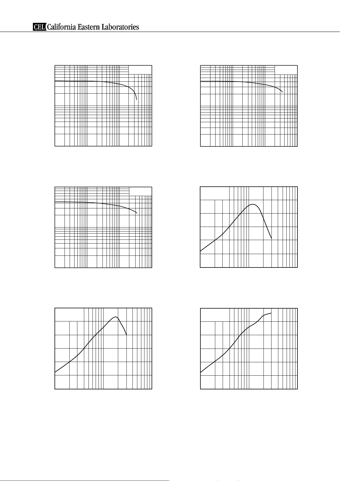
NESG4030M14
DC CURRENT GAIN vs.
COLLECTOR CURRENT
1 000
FE
100
DC Current Gain h
10
DC CURRENT GAIN vs.
COLLECTOR CURRENT
1 000
FE
VCE = 1 V
10.1 10 100
Collector Current IC (mA)
CE
V
= 3 V
DC CURRENT GAIN vs.
COLLECTOR CURRENT
1 000
FE
100
DC Current Gain h
10
GAIN BANDWIDTH PRODUCT
vs. COLLECTOR CURRENT
30
VCE = 1 V,
f = 2 GHz
25
(GHz)
T
20
V
CE
10.1 10 100
Collector Current IC (mA)
= 2 V
100
DC Current Gain h
10
10.1 10 100
Collector Current IC (mA)
GAIN BANDWIDTH PRODUCT
vs. COLLECTOR CURRENT
30
VCE = 2 V,
f = 2 GHz
25
(GHz)
T
20
15
10
5
Gain Bandwidth Product f
0
Collector Current IC (mA)
Remark The graphs indicate nominal characteristics.
101 100
15
10
5
Gain Bandwidth Product f
0
Collector Current IC (mA)
GAIN BANDWIDTH PRODUCT
vs. COLLECTOR CURRENT
30
VCE = 3 V,
f = 2 GHz
25
(GHz)
T
20
15
10
5
Gain Bandwidth Product f
0
Collector Current IC (mA)
101 100
101 100
Data Sheet PU10728EJ02V0DS
5
Page 6
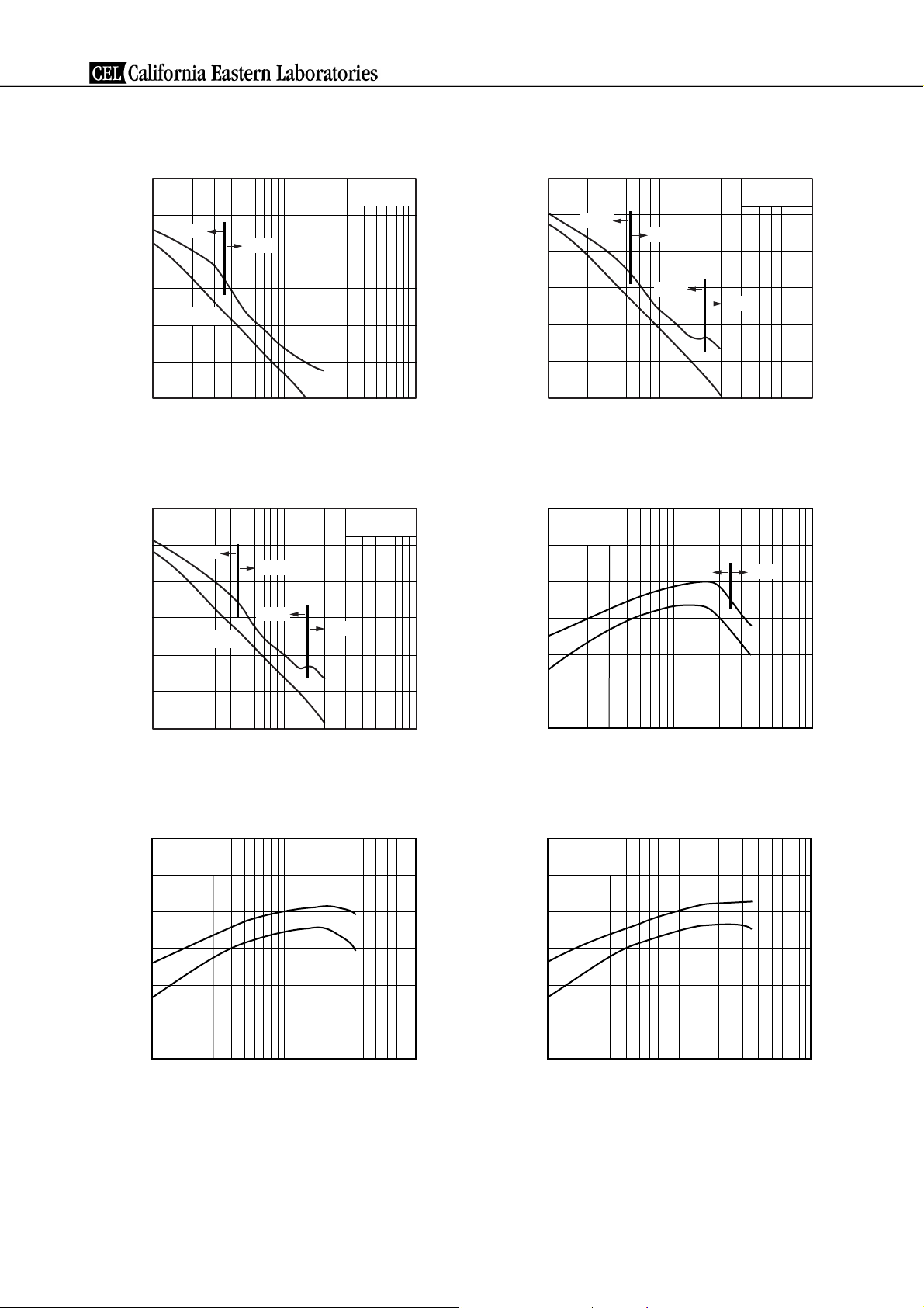
NESG4030M14
INSERTION POWER GAIN,
MAG, MSG vs. FREQUENCY
30
25
MAG
(dB)
2
|
21e
20
MSG
15
2
|S
21e
10
|
5
Insertion Power Gain |S
1 10 100
0
Maximum Available Power Gain MAG (dB)
Maximum Stable Power Gain MSG (dB)
Frequency f (GHz)
INSERTION POWER GAIN,
MAG, MSG vs. FREQUENCY
30
(dB)
2
|
21e
25
20
15
10
MSG
|S
21e
MAG
MAG
2
|
MSG
VCE = 1 V,
C
= 20 mA
I
VCE = 3 V,
C
= 20 mA
I
INSERTION POWER GAIN,
MAG, MSG vs. FREQUENCY
30
25
MSG
MAG
20
(dB)
2
|
21e
15
|S
21e
MAG
2
|
10
5
0
Maximum Available Power Gain MAG (dB)
Maximum Stable Power Gain MSG (dB)
Insertion Power Gain |S
1 10 100
Frequency f (GHz)
INSERTION POWER GAIN, MAG, MSG
vs. COLLECTOR CURRENT
30
VCE = 1 V,
f = 2.4 GHz
25
(dB)
|
21e
20
15
10
|S
2
21e
2
|
VCE = 2 V,
IC = 20 mA
MSG
MAGMSG
5
Insertion Power Gain |S
1 10 100
0
Maximum Available Power Gain MAG (dB)
Maximum Stable Power Gain MSG (dB)
Frequency f (GHz)
INSERTION POWER GAIN, MSG
vs. COLLECTOR CURRENT
30
VCE = 2 V,
f = 2.4 GHz
25
(dB)
20
2
|
21e
15
10
5
0
Maximum Stable Power Gain MSG (dB)
Insertion Power Gain |S
1 10 100
Collector Current I
Remark The graphs indicate nominal characteristics.
MSG
|S
21e
2
|
C
(mA)
5
0
Maximum Available Power Gain MAG (dB)
Maximum Stable Power Gain MSG (dB)
Insertion Power Gain |S
1 10 100
Collector Current IC (mA)
INSERTION POWER GAIN, MSG
vs. COLLECTOR CURRENT
30
VCE = 3 V,
f = 2.4 GHz
25
MSG
(dB)
20
2
|
21e
15
10
5
0
Maximum Stable Power Gain MSG (dB)
Insertion Power Gain |S
1 10 100
Collector Current I
|S
21e
2
|
C
(mA)
6
Data Sheet PU10728EJ02V0DS
Page 7
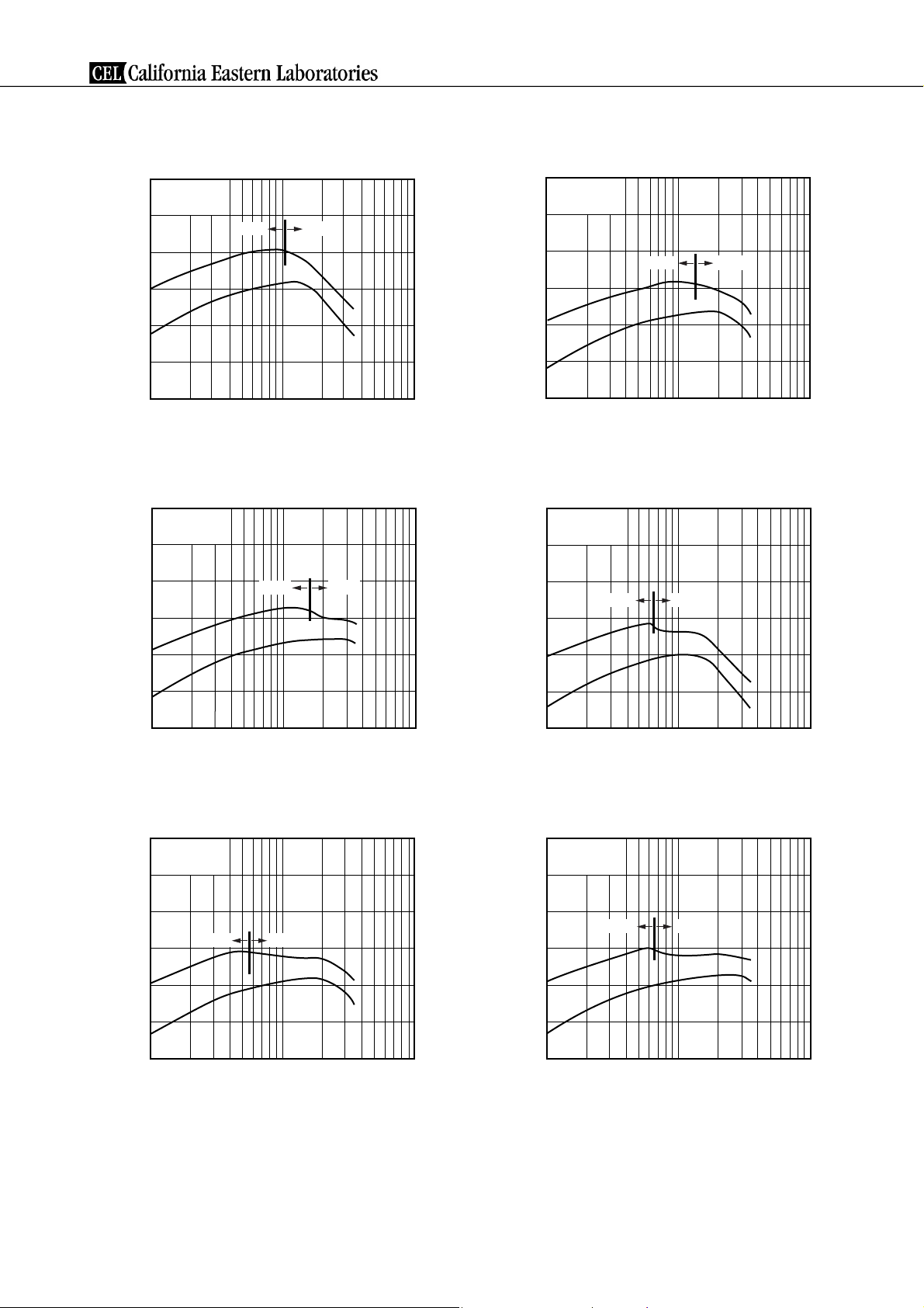
NESG4030M14
INSERTION POWER GAIN, MAG, MSG
vs. COLLECTOR CURRENT
25
VCE = 1 V,
f = 5.2 GHz
20
(dB)
15
2
|
21e
10
|S
5
0
–5
Maximum Available Power Gain MAG (dB)
Maximum Stable Power Gain MSG (dB)
Insertion Power Gain |S
1 10 100
Collector Current IC (mA)
INSERTION POWER GAIN, MAG, MSG
vs. COLLECTOR CURRENT
30
VCE = 3 V,
f = 5.2 GHz
25
(dB)
20
2
|
21e
15
21e
INSERTION POWER GAIN, MAG, MSG
vs. COLLECTOR CURRENT
30
V
CE
= 2 V,
f = 5.2 GHz
25
MAGMSG
(dB)
|
21e
20
MAGMSG
2
15
2
|
10
2
|S
21e
|
5
Insertion Power Gain |S
1 10 100
0
Maximum Available Power Gain MAG (dB)
Maximum Stable Power Gain MSG (dB)
Collector Current IC (mA)
INSERTION POWER GAIN, MAG, MSG
vs. COLLECTOR CURRENT
30
V
CE
= 1 V,
f = 5.8 GHz
25
(dB)
|
21e
20
MAGMSG
15
MAGMSG
2
10
2
|S
21e
|
5
Insertion Power Gain |S
1 10 100
0
Maximum Available Power Gain MAG (dB)
Maximum Stable Power Gain MSG (dB)
Collector Current IC (mA)
INSERTION POWER GAIN, MAG, MSG
vs. COLLECTOR CURRENT
30
VCE = 2 V,
f = 5.8 GHz
25
(dB)
20
2
|
21e
15
10
5
Insertion Power Gain |S
1 10 100
0
Maximum Available Power Gain MAG (dB)
Maximum Stable Power Gain MSG (dB)
Collector Current IC (mA)
Remark The graphs indicate nominal characteristics.
MAGMSG
2
|S
21e
|
10
|S
5
Insertion Power Gain |S
1 10 100
0
Maximum Available Power Gain MAG (dB)
Maximum Stable Power Gain MSG (dB)
Collector Current I
INSERTION POWER GAIN, MAG, MSG
vs. COLLECTOR CURRENT
30
VCE = 3 V,
f = 5.8 GHz
25
(dB)
2
20
|
21e
MAGMSG
15
10
|S
5
Insertion Power Gain |S
1 10 100
0
Maximum Available Power Gain MAG (dB)
Maximum Stable Power Gain MSG (dB)
Collector Current IC (mA)
21e
21e
2
|
2
|
C
(mA)
Data Sheet PU10728EJ02V0DS
7
Page 8
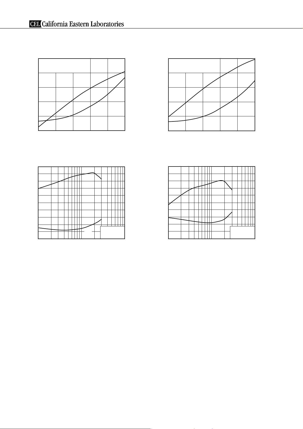
NESG4030M14
OUTPUT POWER, COLLECTOR
CURRENT vs. INPUT POWER
20
f = 2.4 GHz , VCE = 2 V,
I
C (set)
= 6 mA
15
(dBm)
out
10
P
out
5
I
Output Power P
0
–5
–20 –10 –5 0–15 5
C
Input Power Pin (dBm)
NOISE FIGURE, ASSOCIATED GAIN
vs. COLLECTOR CURRENT
5
G
4
3
a
50
40
(mA)
C
30
20
Collector Current I
10
0
20
16
(dB)
a
12
OUTPUT POWER, COLLECTOR
CURRENT vs. INPUT POWER
15
f = 5.8 GHz , VCE = 2 V,
I
C (set)
= 6 mA
10
P
(dBm)
out
5
out
0
I
C
Output Power P
–5
–10
–15 –5 –0 5–10 10
Input Power Pin (dBm)
NOISE FIGURE, ASSOCIATED GAIN
vs. COLLECTOR CURRENT
5
G
4
3
a
50
40
(mA)
C
30
20
10
Collector Current I
0
15
12
(dB)
a
9
2
Noise Figure NF (dB)
1
0
<R>
S-PARAMETERS
of the parameters to microwave circuit simulators without the need for keyboard inputs.
NF
f = 2.4 GHz,
V
CE
= 2 V
1 10 100
Collector Current IC (mA)
8
Associated Gain G
4
0
2
Noise Figure NF (dB)
1
0
1 10 100
NF
f = 5.8 GHz,
V
Collector Current IC (mA)
CE
= 2 V
6
3
0
Remark The graphs indicate nominal characteristics.
S-parameters and noise parameters are provided on our Web site in a format (S2P) that enables the direct import
Click here to download S-parameters.
[RF and Microwave] → [Device Parameters]
URL http://www.necel.com/microwave/en/
Associated Gain G
8
Data Sheet PU10728EJ02V0DS
Page 9
NESG4030M14
<R>
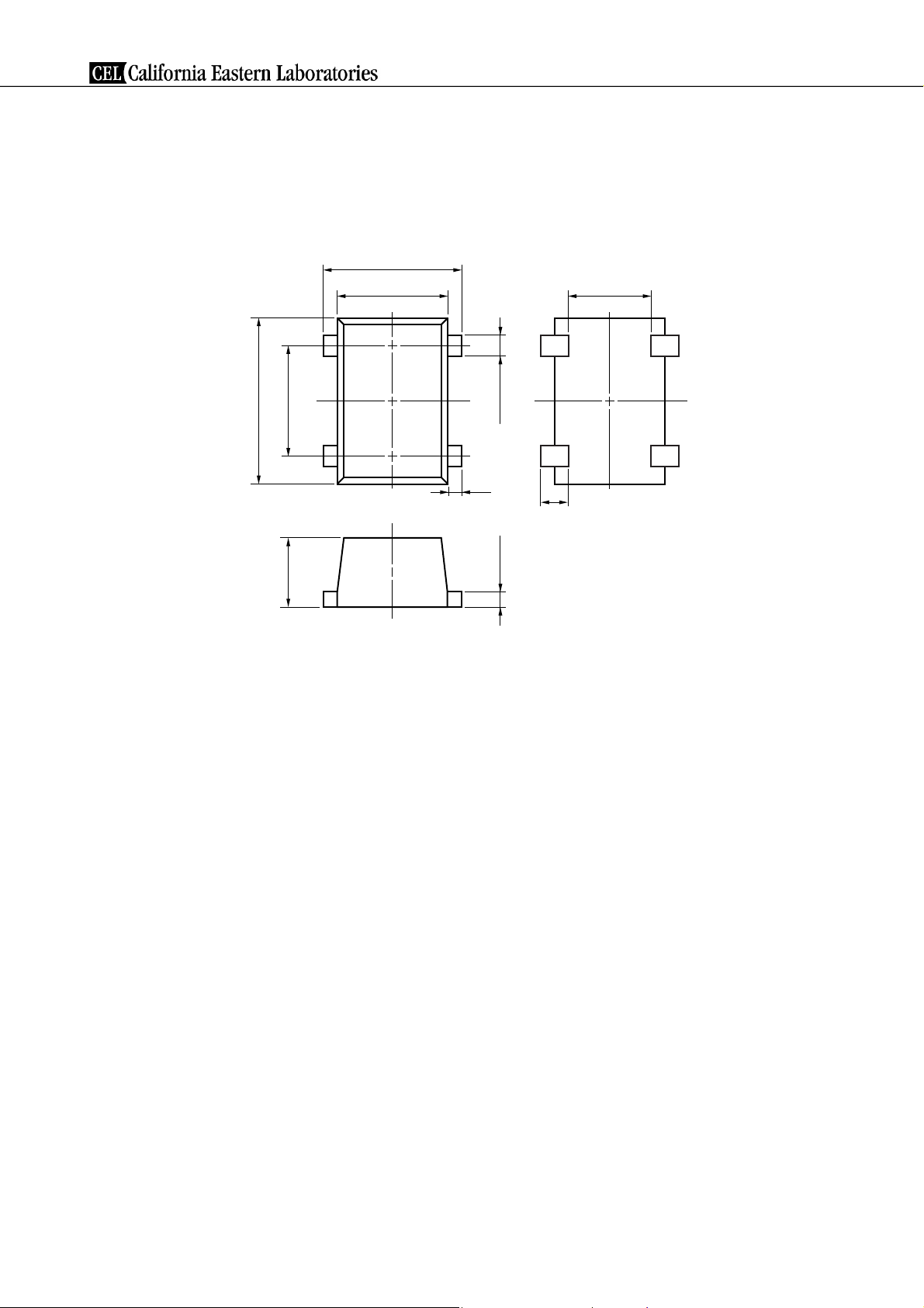
PACKAGE DIMENSIONS
4-PIN LEAD-LESS MINIMOLD (M14, 1208 PKG) (UNIT: mm)
(Top View)
1.0±0.05
+0.07
0.8
–0.05
–0.05
+0.07
0.8
1.2
0.5±0.05
zK
43
12
0.1
0.15±0.05
–0.05
+0.1
0.11
(Bottom View)
0.6
0.2
PIN CONNECTIONS
1. Collector
2. Emitter
3. Base
4. Emitter
Data Sheet PU10728EJ02V0DS
9
Page 10

NESG4030M14
•
The information in this document is current as of August, 2009. The information is subject to
change without notice. For actual design-in, refer to the latest publications of NEC Electronics data
sheets, etc., for the most up-to-date specifications of NEC Electronics products. Not all products
and/or types are available in every country. Please check with an NEC Electronics sales
representative for availability and additional information.
•
No part of this document may be copied or reproduced in any form or by any means without the prior
written consent of NEC Electronics. NEC Electronics assumes no responsibility for any errors that may
appear in this document.
•
NEC Electronics does not assume any liability for infringement of patents, copyrights or other intellectual
property rights of third parties by or arising from the use of NEC Electronics products listed in this document
or any other liability arising from the use of such products. No license, express, implied or otherwise, is
granted under any patents, copyrights or other intellectual property rights of NEC Electronics or others.
•
Descriptions of circuits, software and other related information in this document are provided for illustrative
purposes in semiconductor product operation and application examples. The incorporation of these
circuits, software and information in the design of a customer's equipment shall be done under the full
responsibility of the customer. NEC Electronics assumes no responsibility for any losses incurred by
customers or third parties arising from the use of these circuits, software and information.
•
While NEC Electronics endeavors to enhance the quality and safety of NEC Electronics products, customers
agree and acknowledge that the possibility of defects thereof cannot be eliminated entirely. In addition, NEC
Electronics products are not taken measures to prevent radioactive rays in the product design. When customers
use NEC Electronics products with their products, customers shall, on their own responsibility, incorporate
sufficient safety measures such as redundancy, fire-containment and anti-failure features to their products in
order to avoid risks of the damages to property (including public or social property) or injury (including death) to
persons, as the result of defects of NEC Electronics products.
•
NEC Electronics products are classified into the following three quality grades: "Standard", "Special" and
"Specific".
The "Specific" quality grade applies only to NEC Electronics products developed based on a customerdesignated "quality assurance program" for a specific application. The recommended applications of an NEC
Electronics product depend on its quality grade, as indicated below. Customers must check the quality grade of
each NEC Electronics product before using it in a particular application.
"Standard":
"Special":
"Specific":
Computers, office equipment, communications equipment, test and measurement equipment, audio
and visual equipment, home electronic appliances, machine tools, personal electronic equipment
and industrial robots.
Transportation equipment (automobiles, trains, ships, etc.), traffic control systems, anti-disaster
systems, anti-crime systems, safety equipment and medical equipment (not specifically designed
for life support).
Aircraft, aerospace equipment, submersible repeaters, nuclear reactor control systems, life
support systems and medical equipment for life support, etc.
The quality grade of NEC Electronics products is "Standard" unless otherwise expressly specified in NEC
Electronics data sheets or data books, etc. If customers wish to use NEC Electronics products in applications
not intended by NEC Electronics, they must contact an NEC Electronics sales representative in advance to
determine NEC Electronics' willingness to support a given application.
(Note)
(1)
"NEC Electronics" as used in this statement means NEC Electronics Corporation and also includes its
majority-owned subsidiaries.
(2)
"NEC Electronics products" means any product developed or manufactured by or for NEC Electronics (as
defined above).
M8E0904E
 Loading...