

查询NE680M03供应商
PRELIMINARY DATA SHEET
NE680M03NPN SILICON TRANSISTOR
FEATURES
• NEW M03 PACKAGE:
• Smallest transistor outline package available
• Low profile/0.59 mm package height
• Flat lead style for better RF performance
• HIGH GAIN BANDWIDTH PRODUCT:
f
T = 8 GHz
• LOW NOISE FIGURE:
NF = 1.9 dB at 2 GHz
DESCRIPTION
The NE680M03 transistor is designed for low noise, high gain,
and low cost applications. This high f
T part is ideal for low
voltage/low current applications. NEC's new low profile/flat
lead style "M03" package is ideal for today's portable wireless
applications. The NE680 is also available in chip, Micro-x, and
six different low cost plastic surface mount package styles.
ELECTRICAL CHARACTERISTICS (TA = 25°C)
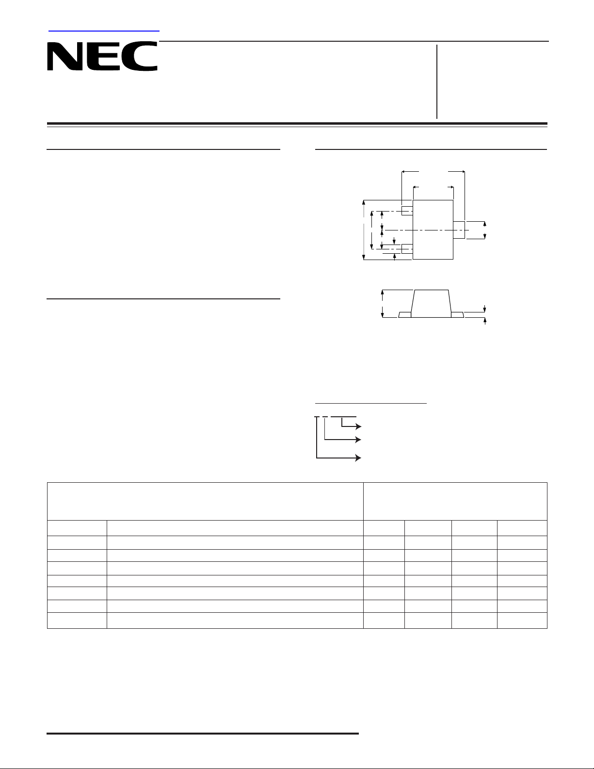
OUTLINE DIMENSIONS
PACKAGE OUTLINE M03
1.2±0.05
0.8±0.1
2
1.4 ±0.1
Note:
1. This dimension was changed
effective 04/2000 from 1.4 mm
to 1.2 mm. Products with "04" or
a higher number indicated for
month of manufacture in lot
numbers have the new dimension.
Example of Lot No. Identification
0 6 xxxxxxx
0.45
(0.9)
0.45
0.2±0.1
0.59±0.05
In-company control code
Month of manufacture
(Example: Jan. = 1, Feb. = 2, etc.
Oct. = X, Nov. = Y, Dec. = Z)
Year of manufacture
(Last digit of year, 2000 = 0)
TH
1
(Units in mm)
0.3±0.1
3
0.15
PIN CONNECTIONS
1. Emitter
2. Base
3. Collector
+0.1
-0.05
PART NUMBER NE680M03
EIAJ1 REGISTERED NUMBER 2SC5434
PACKAGE OUTLINE M03
SYMBOLS PARAMETERS AND CONDITIONS UNITS MIN TYP MAX
fT Gain Bandwidth at VCE = 3 V, IC = 5 mA, f = 2 GHz GHz 5.5 8.0
NF Noise Figure at VCE = 3 V, IC = 6 mA, f = 2 GHz dB 1.9 3.2
2
|S21E|
2
hFE
ICBO Collector Cutoff Current at VCB = 10 V, IE = 0 µA 1.0
IEBO Emitter Cutoff Current at VEB = 1 V, IC = 0 µA 1.0
3
CRE
Notes:
1. Electronic Industrial Association of Japan.
2. Pulsed measurement, pulse width ≤ 350 µs, duty cycle ≤ 2 %.
3. Capacitance is measured with emitter and case connected to the guard terminal at the bridge.
Insertion Power Gain at VCE = 3 V, IC = 5 mA, f = 2 GHz dB 5.5 7.5
Forward Current Gain at VCE = 3 V, IC = 5 mA 80 145
Feedback Capacitance at VCB = 3 V, IE = 0, f = 1 MHz pF 0.3 0.7
California Eastern Laboratories
NE680M03
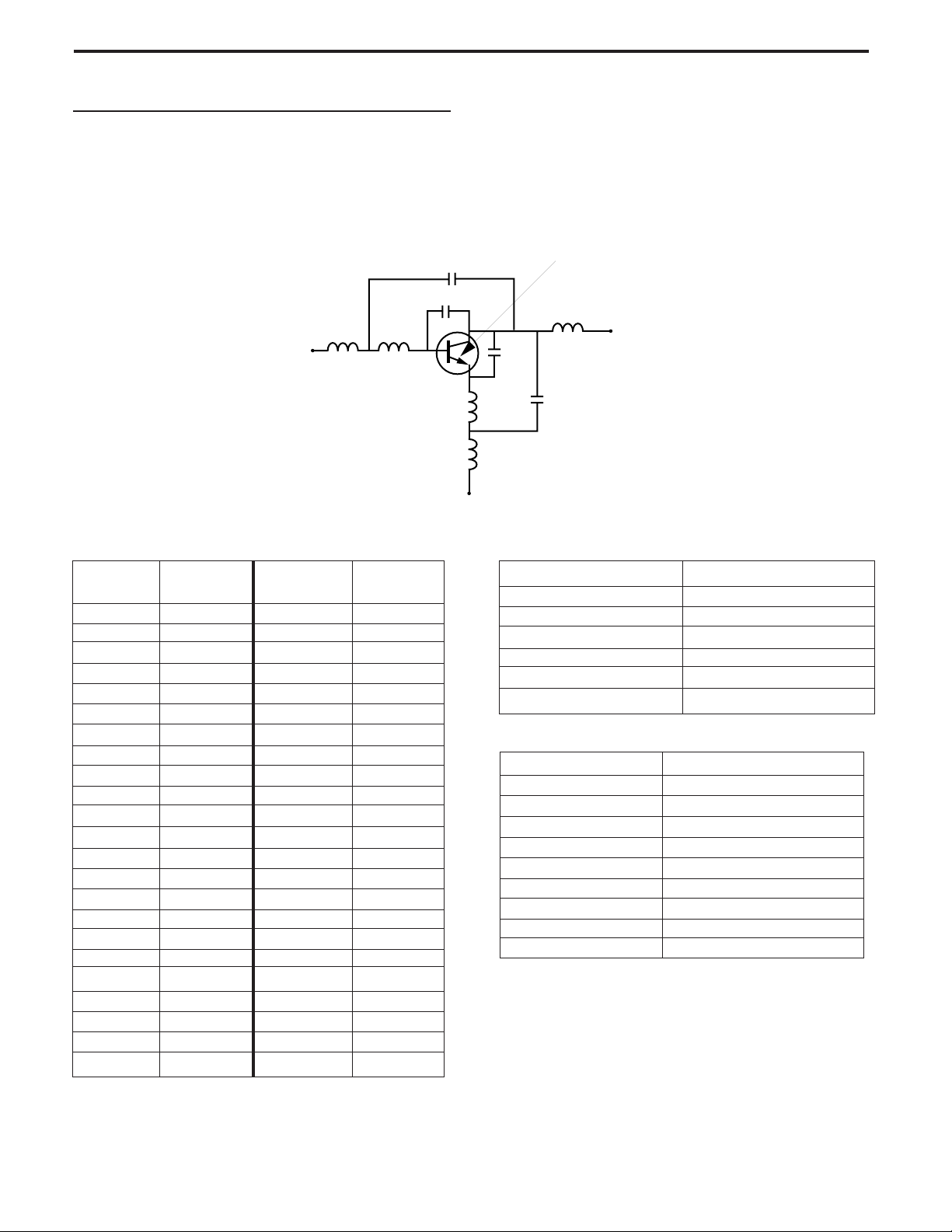
NONLINEAR MODEL
SCHEMATIC
Base
CE
Q1
C
CEPKG
L
CX
Collector
CBPKG
C
C
CB
L
BX
L
B
C
L
E
L
EX
BJT NONLINEAR MODEL PARAMETERS
Parameters Q1 Parameters Q1
IS 5.98e-16 MJC 0.15
BF 179 XCJC 1
NF 1.04 CJS 0
VAF17 VJS 0.75
IKF 0.02 MJS 0
ISE 1.0e-6 FC 0.5
NE 30 TF 8.7e-12
BR 16 XTF 20
NR 1.04 VTF 0.3
VAR 100 ITF 0.04
IKR 6.85e-3 PTF 120
ISC 1.5e-9 TR 0.635e-9
NC 20 EG 1.11
RE 0.50 XTB 0
RB 8.54 XTI 3
RBM 2 KF 0
IRB 4e-4 AF 1
RC 10
CJE 0.358e-12
VJE 0.86
MJE 0.5
CJC 0.162e-12
VJC 0.52
(1)
Emitter
UNITS
Parameter Units
time seconds
capacitance farads
inductance henries
resistance ohms
voltage volts
current amps
ADDITIONAL PARAMETERS
Parameters 680M03
CCB 0.08e-12
CCE 0.08e-12
LB 0.4e-9
LE 0.8e-9
CCBPKG 0.08e-12
CCEPKG 0.08e-12
LBX 0.12e-9
LCX 0.10e-9
LEX 0.12e-9
MODEL RANGE
Frequency: 0.1 to 3.0 GHz
Bias: VCE = 0.5 V to 6 V, IC = 0.5 mA to 15 mA
Date: 11/98
(1) Gummel-Poon Model

NE680M03
ABSOLUTE MAXIMUM RATINGS
1
(TA = 25°C)
SYMBOLS PARAMETERS UNITS RATINGS
CBO Collector to Base Voltage V 20
V
V
CEO Collector to Emitter Voltage V 10
VEBO Emitter to Base Voltage V 1.5
IC Collector Current mA 35
PT Total Power Dissipation mW 125
J Junction Temperature °C 150
T
TSTG Storage Temperature °C -65 to +150
Note:
1. Operation in excess of any one of these parameters may result
in permanent damage.
TYPICAL PERFORMANCE CURVES (TA = 25°C)
COLLECTOR CURRENT vs.
COLLECTOR TO EMITTER VOLTAGE
35
25
(mA)
C
15
FORWARD CURRENT GAIN
vs. COLECTOR CURRENT
500
300
FE
200
100
70
50
VCE = 6 V
30
Collector Current, I
5
0
24 8106
Collector to Emitter Voltage, VCE (V)
Life Support Applications
These NEC products are not intended for use in life support devices, appliances, or systems where the malfunction of these products can reasonably be expected
to result in personal injury. The customers of CEL using or selling these products for use in such applications do so at their own risk and agree to fully indemnify
CEL for all damages resulting from such improper use or sale.
CALIFORNIA EASTERN LABORATORIES • Headquarters • 4590 Patrick Henry Drive • Santa Clara, CA 95054-1817 • (408) 988-3500 • Telex 34-6393 • FAX (408) 988-0279
DATA SUBJECT TO CHANGE WITHOUT NOTICE
EXCLUSIVE NORTH AMERICAN AGENT FOR NEC RF, MICROWAVE & OPTOELECTRONIC SEMICONDUCTORS
Internet: http://WWW.CEL.COM
06/10/2002
20
DC Forward Current Gain, h
10
1 2 3 5 7 10 20 30 50
Collector Current, IC (mA)
 Loading...