

NEC NE4210S01-T1, NE4210S01-T1B Datasheet
DATA SHEET
HETERO JUNCTION FIELD EFFECT TRANSISTOR
NE4210S01
X to Ku BAND SUPER LOW NOISE AMPLIFIER
N-CHANNEL HJ-FET
DESCRIPTION
The NE4210S01 is a Hetero Junction FET that utilizes the hetero junction to create high mobility electrons. Its
excellent low noise and associated gain make it suitable for DBS and another commercial systems.
FEATURES
• Super Low Noise Figure & High Associated Gain
NF = 0.5 dB TYP. Ga = 13.0 dB TYP. @f = 12 GHz
• Gate Length: Lg ≤ 0.20 µm
• Gate Width : Wg = 160 µm
ORDERING INFORMATION (PLAN)
Part Number Marking Supplying Form
NE4210S01-T1 Tape & reel 1 kp/reel
NE4210S01-T1B
Remark
To order evaluation samples, please contact your local NEC sales office. (Part number for sample order:
L
Tape & reel 4 kp/reel
NE4210S01)
ABSOLUTE MAXIMUM RATINGS (TA = +25°C)
Parameter Symbol Ratings Unit
Drain to Source Voltage V
Gate to Source Voltage V
Drain Current I
Gate Current I
Total Power Dissipat i on P
Channel Temperature T
Storage Temperature T
DS
GS
D
G
tot
ch
stg
4.0 V
–3.0 V
DSS
I
100
165 mW
125 °C
–65 to +125 °C
RECOMMENDED OPERATING CONDITIONS (TA = +25°C)
Parameter Symbol MIN. TYP. MAX. Unit
mA
µ
A
Drain to Source Voltage V
Drain Current I
Input Power P
The information in this document is subject to change without notice. Before using this document, please
confirm that this is the latest version.
Not all devices/types available in every country. Please check with local NEC representative for
availability and additional information.
Document No. P14232EJ2V0DS00 (2nd edition)
Date Published November 1999 N CP(K)
Printed in Japan
DS
D
in
The mark shows major revised points.
123V
51015mA
––0dBm
1999©
ELECTRICAL CHARACTERISTICS (TA = +25 °C)
Parameter Symbol Test Conditions MIN. TYP. MAX. Unit
NE4210S01
Gate to Source Leak Current I
Saturated Drain Current I
Gate to Source Cut off Voltage V
Transconductance g
Noise Figure NF – 0.50 0.70 dB
Associated Gain G
GSO
DSS
GS (off)
m
a
VGS = –3 V – 0.5 10
VDS = 2 V, VGS = 0 V 154070mA
VDS = 2 V, IDS = 100 µA –0.2 –0.7 –2.0 V
VDS = 2 V, IDS = 10 mA 40 55 – mS
VDS = 2 V, IDS = 10 mA
f = 12 GHz
11.0 13.0 – dB
µ
A
2
Data Sheet P14232EJ2V0DS00
TYPICAL CHARACTERISTICS (TA = +25 °C)
NE4210S01
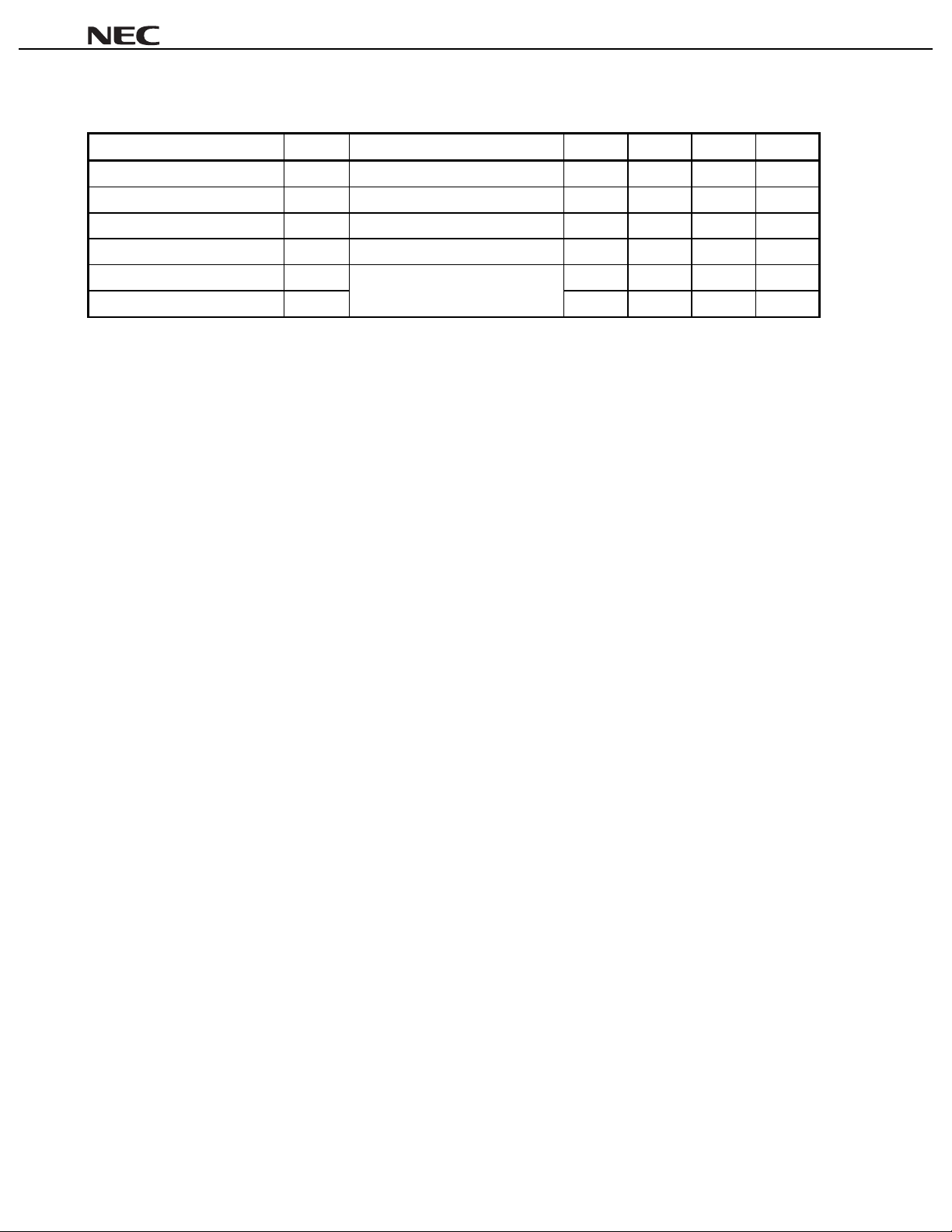
TOTAL POWER DISSIPATION vs.
AMBIENT TEMPERATURE
250
200
(mW)
tot
150
100
50
Total Power Dissipation P
0 50 100 150 200 250
A
Ambient Temperature T
(°C)
DRAIN CURRENT vs.
GATE TO SOURCE VOLTAGE
VDS = 2 V
60
(mA)
D
40
DRAIN CURRENT vs.
DRAIN TO SOURCE VOLTAGE
100
80
(mA)
D
60
40
Drain Current I
20
0 2.01.0
Drain to Source Voltage V
MAXIMUM AVAILABLE GAIN, FORWARD
INSERTION GAIN vs. FREQUENCY
24
(dB)
2
|
21s
20
MSG.
16
VGS = 0 V
–0.2 V
–0.4 V
–0.6 V
DS
(V)
VDS = 2 V
D
= 10 mA
I
MAG.
20
Drain Current I
0
–2.0 –1.0 0
GS
Gate to Source Voltage V
(V)
12
8
Maximum Stable Gain MSG. (dB)
Maximum Available Gain MAG. (dB)
Forward Insertion Gain |S
4
13024 206 8 10 14
2
|S
21S
|
Frequency f (GHz)
Data Sheet P14232EJ2V0DS00
3
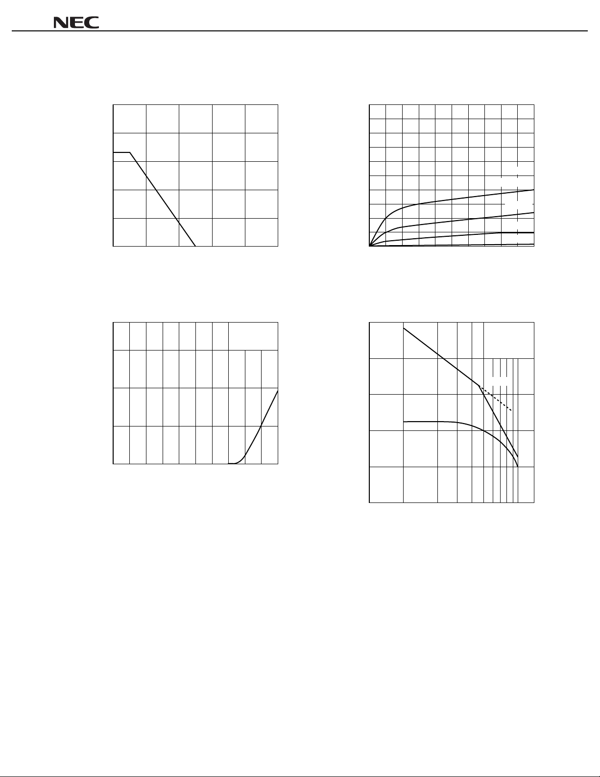
Gain Calculations
NE4210S01
S21
MSG. =
S
S21
MAG. =
S
12
k ±
12
NOISE FIGURE, NF ASSOCIATED GAIN vs.
FREQUENCY
a
G
1.0
Noise Figure NF (dB)
0.5
NF
0
1302
1 + | |2 – |S11 |2 – |S22|
K =
2 |S
k2 – 1 = S11·S22 – S21·S12
∆
∆
VDS = 2 V
D
= 10 mA
I
4206 8 10 14
Frequency f (GHz)
12| |S21|
24
20
(dB)
a
16
12
NF Associated Gain G
8
4
2
NOISE FIGURE, NF ASSOCIATED GAIN vs.
DRAIN CURRENT
VDS = 2 V
f = 12 GHz
2.0
1.5
Noise Figure NF (dB)
1.0
0.5
a
G
NF
Drain Current ID (mA)
15
14
(dB)
a
13
12
11
NF Associated Gain G
3020100
4
Data Sheet P14232EJ2V0DS00

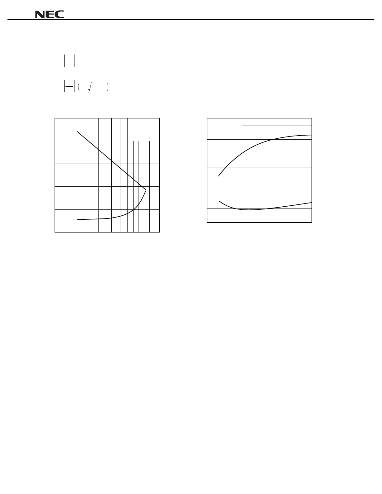
S-PARAMETERS
MAG. AND ANG.
VDS = 2 V, ID = 10 mA
NE4210S01
FREQUENCY S
11
21
S
12
S
S
MHz MAG. ANG. MAG. ANG. MAG. ANG. MAG. ANG.
2000.0000
2500.0000
3000.0000
3500.0000
4000.0000
4500.0000
5000.0000
5500.0000
6000.0000
6500.0000
7000.0000
7500.0000
8000.0000
8500.0000
9000.0000
9500.0000
10000.0000
10500.0000
11000.0000
11500.0000
12000.0000
12500.0000
13000.0000
13500.0000
14000.0000
14500.0000
15000.0000
15500.0000
16000.0000
16500.0000
17000.0000
17500.0000
18000.0000
0.972
0.953
0.934
0.910
0.887
0.865
0.842
0.821
0.802
0.777
0.732
0.685
0.652
0.619
0.591
0.563
0.538
0.517
0.488
0.460
0.433
0.424
0.421
0.436
0.461
0.495
0.528
0.542
0.556
0.561
0.564
0.571
0.581
–21.0
–27.3
–34.1
–40.2
–45.8
–51.1
–55.5
–60.0
–64.8
–70.2
–76.4
–83.4
–91.3
–100.8
–111.0
–120.7
–129.7
–138.8
–148.6
–158.9
–171.3
175.5
161.6
147.9
135.9
125.0
115.2
106.7
99.3
91.0
82.6
74.3
67.3
4.436
4.435
4.443
4.385
4.306
4.244
4.164
4.129
4.122
4.151
4.175
4.179
4.184
4.210
4.189
4.131
4.070
4.023
3.963
3.905
3.850
3.767
3.675
3.551
3.421
3.285
3.151
3.003
2.885
2.764
2.609
2.456
2.297
153.9
147.1
139.9
132.9
126.3
120.0
114.1
108.3
102.6
96.5
89.8
82.9
76.2
69.1
61.5
54.4
47.4
40.3
33.2
26.1
18.5
10.9
3.3
–4.2
–11.5
–18.5
–25.9
–32.3
–39.0
–46.4
–53.3
–59.7
–65.8
0.026
0.033
0.039
0.044
0.047
0.051
0.054
0.057
0.061
0.067
0.071
0.073
0.077
0.082
0.086
0.091
0.094
0.099
0.103
0.104
0.108
0.111
0.113
0.112
0.112
0.113
0.111
0.109
0.108
0.107
0.108
0.106
0.103
73.8
69.6
63.7
60.0
54.4
50.2
46.6
42.8
40.6
37.6
33.0
28.7
25.6
23.0
18.0
13.4
10.7
6.5
1.7
–2.6
–7.1
–11.2
–16.9
–19.9
–24.6
–28.5
–32.0
–33.5
–37.0
–39.4
–42.3
–46.1
–48.0
0.621
0.610
0.592
0.579
0.564
0.554
0.546
0.538
0.531
0.519
0.495
0.460
0.423
0.385
0.344
0.301
0.270
0.250
0.236
0.225
0.215
0.194
0.166
0.144
0.137
0.161
0.210
0.254
0.301
0.347
0.381
0.396
0.400
22
–16.6
–21.6
–27.1
–32.2
–37.2
–41.6
–45.5
–49.4
–52.1
–56.5
–60.5
–63.9
–67.5
–72.2
–78.5
–86.2
–95.5
–107.2
–118.7
–127.6
–137.8
–147.8
–161.6
177.6
151.7
127.6
111.3
104.7
101.1
99.3
96.0
91.6
87.1
Data Sheet P14232EJ2V0DS00
5
 Loading...