NEC MC-9400A Datasheet

DATA SHEET
HYBRID INTEGRATED CIRCUIT
MC-9400A
320 (240)-BIT AC- PDP DRIVER MODULE
DESCRIPTION
The MC-9400A is a PDP driver module that incorporates five 64-bit high breakdown voltage output (150 V, 40 mA)
CMOS driver ICs. It supports 320 outputs in the case of 4-bit parallel input, and 240 outputs in the case of 3-bit parallel
input.
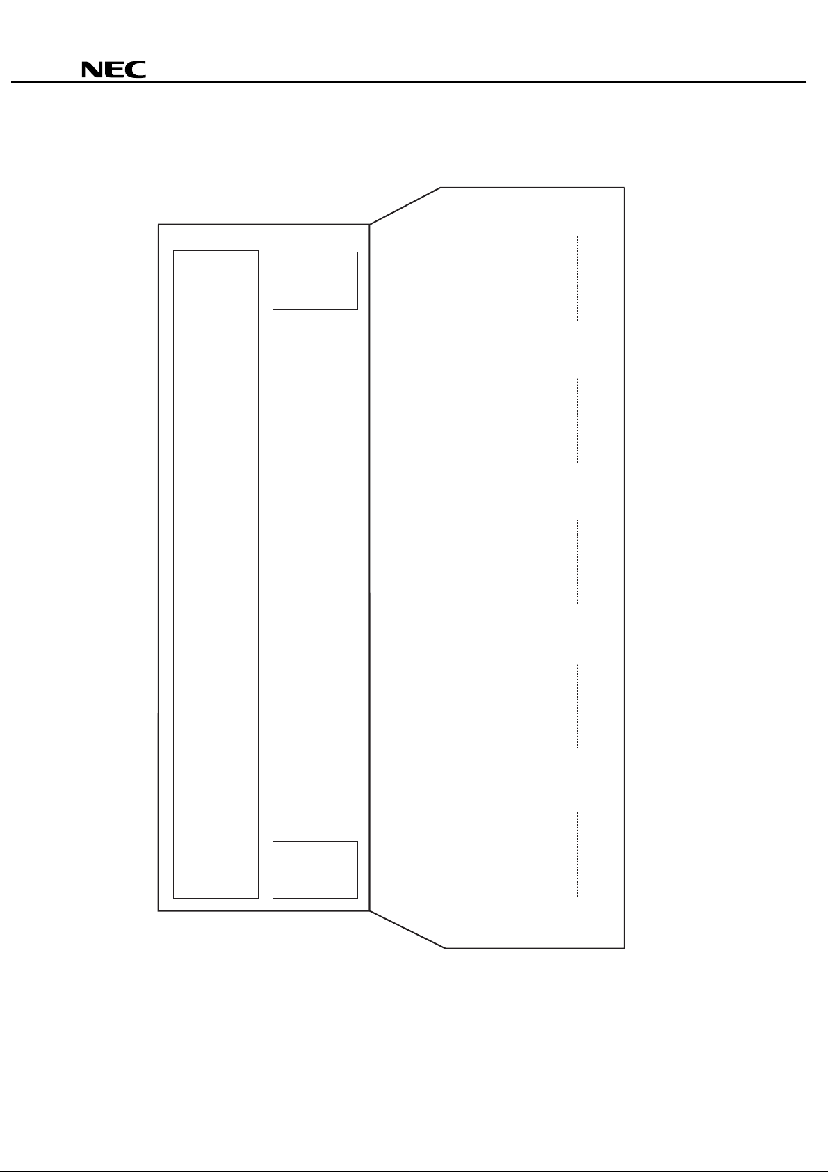
The integrated structure of the MC-9400A, which combines a COB with an aluminum heat sink and an output flexible
printed circuit (FPC) board, enables the easy implementation of heat dissipation measures and high-density mounting.
FEATURES
• Incorporates five µPD16337s with four 16-bit bi-directional shift registers
• Low thermal resistance realized by chip-on-metal structure
• Provided with connector and capacitor for easy mounting on a panel
• Supports output electrode with a narrow pitch through use of a flexible printed circuit board
• Polarity of all driver outputs can be inverted through use of /PC pins
• Supports custom modules
Remark
/XXX indicates active low.
ORDERING INFORMATI O N
Part Number Package
MC-9400A COB
The information in this document is subject to change without notice.
Document No. S13787EJ2V0DS00 (2nd edition)
Data Published October 1998 NS CP(K)
Printed in Japan
The mark
★★★★
shows major revised points.
© NEC Corporation 1998

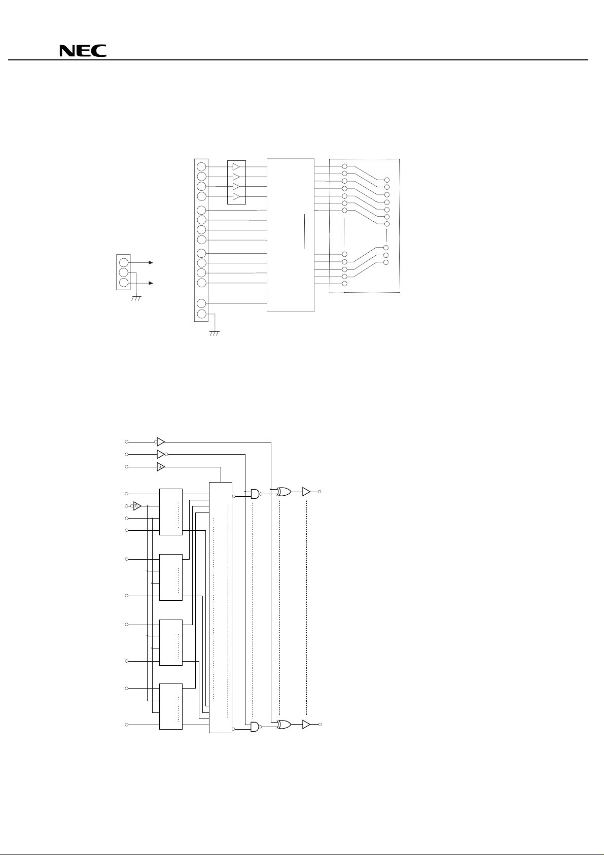
BLOCK DIAGRAM (1/ 5 CIRCUIT)
CN3
CN1,2
V
DD1
(Logic power supply)
VDD2
(Driver power supply)
74AC244
µ
PD16337
/PC O1
BLK
LE
R,/L
1
A
A2
A3
A4
B1
B2
B3
B4
/CLK
O2
O3
O4
O5
O6
O7
O60
O61
O62
O63
O64
MC-9400A
Remark
PD16337s incorporated : 240 outputs at 3 ch and 320 outputs at 4 ch.
Five
µ
See the following block diagram for the
PD16337 BLOCK DIAGRAM
µµµµ
/PC
BLK
LE
SR1
A
1
/CLK CLK
R,/L R,/L
B
1
A
2
B
2
A
3
B
3
A
B
A
CLK
R,/L
B
A
CLK
R,/L
B
S
1
1
5
S
S
61
1
SR2
S
2
2
6
S
S
62
2
SR3
S
3
3
7
S
S
63
3
PD16337.
µ
LE
/L
1
S
1
S
2
S
3
S
4
Note
O
1
2
A
4
B
4
SRn : 16-bit shift register
Note
SR4
S
A
4
4
8
S
CLK
R,/L
B
S
64
4
S
61
S
62
S
63
S
64
/L
64
S
High breakdown voltage CMOS driver 150V, ±40 mA(MAX.).
64

★
PIN CONFIGURATION ( Top Vi ew)
CN3
B
54
B
53
B
52
B
51
A
51
A
52
A
53
A
54
B
44
B
43
B
42
B
41
A
41
A
42
A
43
A
44
GND 34
/CLK 33
GND 32
LE 31
GND 30
R,/L 29
GND 28
/PC 27
GND 26
BLK 25
B
34
B
33
B
32
B
31
A
31
A
32
A
33
A
34
B
24
B
23
B
22
B
21
A
21
A
22
A
23
A
24
B
14
B
13
B
12
B
11
A
11
A
12
A
13
A
14
50
49
48
47
46
45
44
43
42
41
40
39
38
37
36
35
24
23
22
21
20
19
18
17
16
15
14
13
12
11
10
9
8
7
6
5
4
3
2
1
CN2
V
DD2
1
GND 2
V
DD1
3
CN1
V
DD2
1
GND 2
V
DD1
3
EPC
O
O
O
O
O
O
O
O
O
O
MC-9400A
320
257
256
194
193
129
128
65
64
1
Caution To prevent latch-up breakage, be sure to turn the power on in the order of V
signal, and V
DD2
, and turn the power off in the reverse order. Keep this order also during
a transition period.
DD1
, logic
3

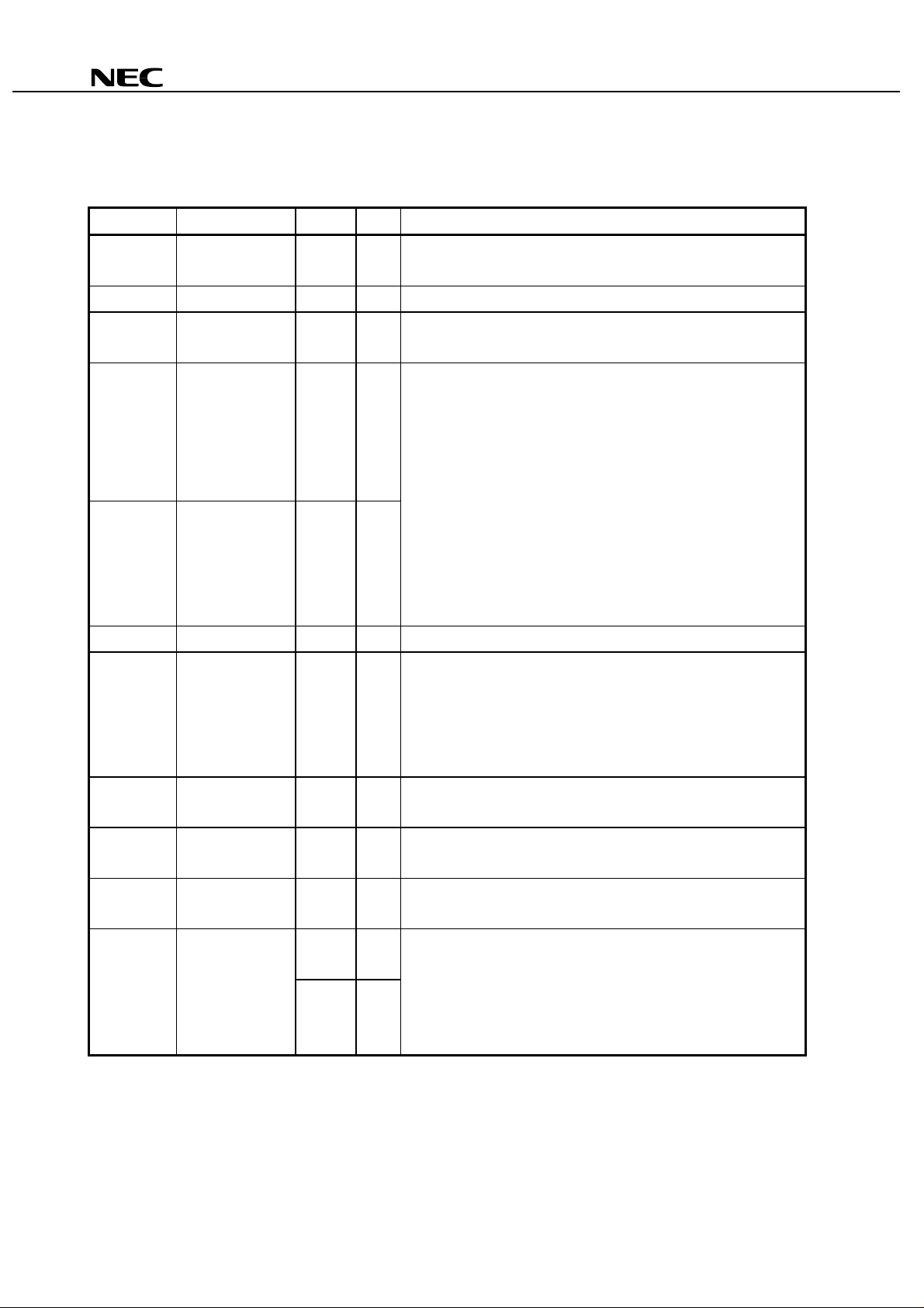
PIN FUNCTIONS
Pin Symbol Pin Name Pin No. I/O Description
MC-9400A
/PC Polarity inverted
27 CN3 /PC = L : Polarity of all outputs inverted
input
BLK Blanking input 25 CN3 BLK = H : All outputs = H or L
LE Latch enable input 31 CN3 Automatically latches by a high level input at the rising edge of the
clock
A11 to A14,
21
to A24,
A
31
to A34,
A
41
to A44,
A
51
to A
A
B11 to B14,
21
to B24,
B
31
to B34,
B
41
to B44,
B
51
to B
B
RIGHT data input 1 to 4
54
LEFT data input 5 to 8
54
9 to 12
17 to 20
35 to 38
46
13 to 16
21 to 24
39 to 42
47 to 50
CN3
CN3
When R,/L = H
11
to A14, A21 to A24, A31 to A34, A41 to A44, A51 to A
A
11
to B14, B21 to B24, B31 to B34, B41 to B44, B51 to B
B
When R,/L = L
11
to A14, A21 to A24, A31 to A34, A41 to A44, A51 to A
A
11
to B14, B21 to B24, B31 to B34, B41 to B44, B51 to B
B
54
: Input
54
: Output
54
: Output
54
: Input
/CLK Clock i nput 33 CN3 Executes a shi ft at the rising edge
R,/L Shi f t control input 29 CN3
Right shift mode by H
→
1
1
1
SR
: A
61
... S
S
→
1
(SR2, SR3, and SR4 also same direction)
B
Left shift mode by L
→
1
1
: B
SR
S
61
... S
→
1
1
(SR2, SR3, and SR4 also same direction)
A
320
O1 to O
High breakdown
voltage output
DD1
V
Logic block power
supply
DD2
V
Driver block power
supply
GND Ground
4
1 to 320 FPC 150 V, 40mA (MA X.)
1 CN1
5 V ± 10 %
CN2
3 CN1
30 V to 130 V
CN2
2 CN1
Connected to system ground
CN2
26,28,
CN3
30,32,
34

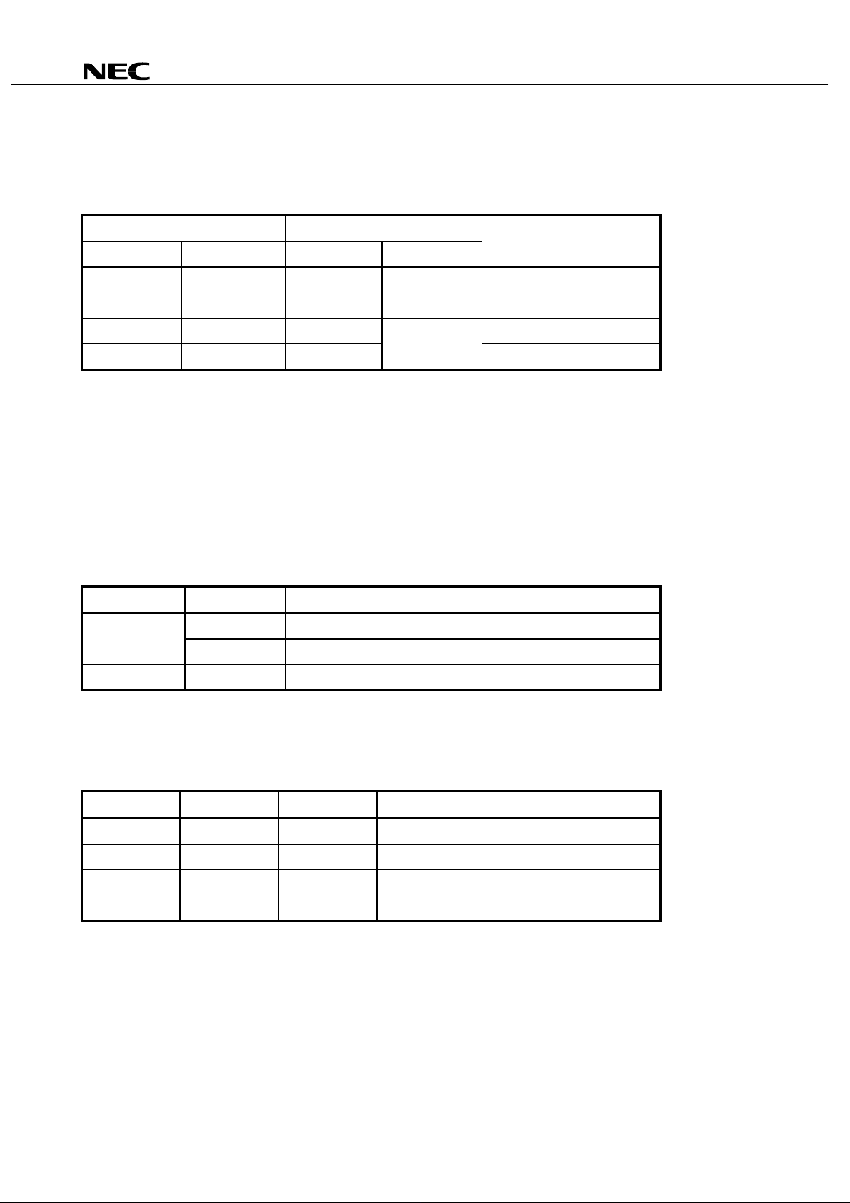
TRUTH TABLE
1. Shift register block
Input Output
R,/L /CLK A B
↓
↓
Input
Output
57
, S58, S59, and S60 are shifted to S61, S62, S63, and S64, and output from B1, B2, B3,
Note2
Notes 1.
2.
H
HX
L
L X Output
On a clock rise, the data S
and B4, respectively.
On a clock fall, the data S5, S6, S7, and S8 are shifted to S1, S2, S3, and S4, and output from A1, A2, A3, and A4,
respectively.
Output
Output Retain
Input
Note1
Execution of right s hi f t
Execution of left s hi ft
Retain
MC-9400A
Shift register
Remark
X= H or L, H= High level, L= Low level
2. Latch block
LE /CLK Output state of latc h bl ock (/Ln)
Remark
H
↓
↓
L X Retains the latch data
X= H or L, H= High level, L= Low level
Latches the data of Sn and retai ns the output data
Retains the latch data
3. Driver block
/Ln BLK /PC Driver output state
X H H H (all driver outputs : H)
X H L L (all driver outputs : L)
X L H Outputs latch data (/Ln)
X L L Outputs latch data (/Ln) with polarity inverted
Remark
X= H or L, H= High level, L= Low level
5
 Loading...