

NEC MC-4R96CEE6C-653, MC-4R96CEE6C-745, MC-4R96CEE6C-845, MC-4R96CEE6B-653, MC-4R96CEE6B-745 Datasheet

PRELIMINARY DATA SHEET
MOS INTEGRATED CIRCUIT
MC-4R96CEE6B, 4R96CEE6C
Direct RambusTM DRAM RIMMTM Module
96M-BYTE (48M-WORD x 16-BIT)
Description
The Direct Rambus RIMM module is a general-purpose high-performance memory module subsystem suitable for
use in a broad range of applications including computer memory, personal computers, workstations, and other
applications where high bandwidth and low latency are required.
MC-4R96CEE6B, 4R96CEE6C modules consists of six 128M Direct Rambus DRAM (Direct RDRAM™) devices
(
µ
PD488448). These are extremely high-speed CMOS DRAMs organized as 8M words by 16 bits. The use of
Rambus Signaling Level (RSL) technology permits 600MHz, 711MHz or 800MHz transfer rates while using
conventional system and board design technologies.
Direct RDRAM devices are capable of sustained data transfers at 1.25 ns per two bytes (10 ns per sixteen bytes).
The architecture of the Direct RDRAM enables the highest sustained bandwidth for multiple, simultaneous,
randomly addressed memory transactions. The separate control and data buses with independent row and column
control yield over 95 % bus efficiency. The Direct RDRAM's 32 banks support up to four simultaneous transactions
per device.
Features
• 184 edge connector pads with 1mm pad spacing
• 96 MB Direct RDRAM storage
• Each RDRAM
• Gold plated contacts
• RDRAMs use Chip Scale Package (CSP)
• Serial Presence Detect support
• Operates from a 2.5 V supply
• Low power and powerdown self refresh modes
• Separate Row and Column buses for higher efficiency
has 32 banks, for 192 banks total on module
The information in this document is subject to change without notice. Before using this document, please
confirm that this is the latest version.
Not all devices/types available in every country. Please check with local NEC representative for
availability and additional information.
Document No. M14538EJ1V1DS00 (1st edition)
Date Published November 1999 NS CP (K)
Printed in Japan
The mark
★★★★
shows major revised points.
©
1999

Order information
MC-4R96CEE6B, 4R96CEE6C
Part number Organization I/O Freq.
MHz
MC-4R96CEE6B - 845 48M x 16 800 45 184 edge connector pads RIMM 6 pieces of
MC-4R96CEE6B - 745 711 45 with heat spreader
MC-4R96CEE6B - 653 600 53 Edge connector : Gold plated FBGA (D2BGATM) package
MC-4R96CEE6C - 845 800 45 6 pieces of
MC-4R96CEE6C - 745 711 45
MC-4R96CEE6C - 653 600 53 FBGA (µBGA) package
RAS access time
ns
Package Mounted devices
PD488448FB
µ
PD488448FF
µ
2
Preliminary Data Sheet M14538EJ1V1DS00
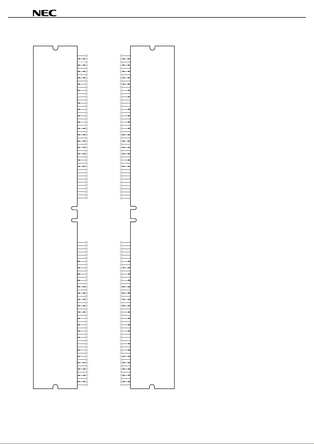
Module Pad Configuration
MC-4R96CEE6B, 4R96CEE6C
B10
B11
B12
B13
B14
B15
B16
B17
B18
B19
B20
B21
B22
B23
B24
B25
B26
B27
B28
B29
B30
B31
B32
B33
B34
B35
B36
B37
B38
B39
B40
B41
B42
B43
B44
B45
B46
B1
B2
B3
B4
B5
B6
B7
B8
B9
GND
LDQA7
GND
LDQA5
GND
LDQA3
GND
LDQA1
GND
LCFM
GND
LCFMN
GND
NC
GND
LROW2
GND
LROW0
GND
LCOL3
GND
LCOL1
GND
LDQB0
GND
LDQB2
GND
LDQB4
GND
LDQB6
GND
LDQB8
GND
LCMD
CMOS
V
SIN
CMOS
V
NC
GND
NC
V
DD
V
DD
NC
NC
NC
NC
GND
LDQA8
GND
LDQA6
GND
LDQA4
GND
LDQA2
GND
LDQA0
GND
LCTMN
GND
LCTM
GND
NC
GND
LROW1
GND
LCOL4
GND
LCOL2
GND
LCOL0
GND
LDQB1
GND
LDQB3
GND
LDQB5
GND
LDQB7
GND
LSCK
V
CMOS
SOUT
V
CMOS
NC
GND
NC
V
V
NC
NC
NC
NC
A1
A2
A3
A4
A5
A6
A7
A8
A9
A10
A11
A12
A13
A14
A15
A16
A17
A18
A19
A20
A21
A22
A23
A24
A25
A26
A27
A28
A29
A30
A31
A32
A33
A34
A35
A36
A37
A38
A39
DD
DD
A40
A41
A42
A43
A44
A45
A46
Side B Side A
B47
B48
B49
B50
B51
B52
B53
B54
B55
B56
B57
B58
B59
B60
B61
B62
B63
B64
B65
B66
B67
B68
B69
B70
B71
B72
B73
B74
B75
B76
B77
B78
B79
B80
B81
B82
B83
B84
B85
B86
B87
B88
B89
B90
B91
B92
NC
NC
NC
NC
V
REF
GND
SA0
DD
V
SA1
DD
SV
SA2
DD
V
RCMD
GND
RDQB8
GND
RDQB6
GND
RDQB4
GND
RDQB2
GND
RDQB0
GND
RCOL1
GND
RCOL3
GND
RROW0
GND
RROW2
GND
NC
GND
RCFMN
GND
RCFM
GND
RDQA1
GND
RDQA3
GND
RDQA5
GND
RDQA7
GND
NC
NC
NC
NC
V
REF
GND
SCL
V
SDA
SV
SWP
V
RSCK
GND
RDQB7
GND
RDQB5
GND
RDQB3
GND
RDQB1
GND
RCOL0
GND
RCOL2
GND
RCOL4
GND
RROW1
GND
NC
GND
RCTM
GND
RCTMN
GND
RDQA0
GND
RDQA2
GND
RDQA4
GND
RDQA6
GND
RDQA8
GND
A47
A48
A49
A50
A51
A52
DD
DD
DD
A53
A54
A55
A56
A57
A58
A59
A60
A61
A62
A63
A64
A65
A66
A67
A68
A69
A70
A71
A72
A73
A74
A75
A76
A77
A78
A79
A80
A81
A82
A83
A84
A85
A86
A87
A88
A89
A90
A91
A92
LCFM, LCFMN,
RCFM, RCFMN : Clock from master
LCTM, LCTMN,
RCTM, RCTMN : Clock to master
LCMD, RCMD : Serial Command Pad
LROW2 - LROW0,
RROW2 - RROW0 : Row bus
LCOL4 - LCOL0,
RCOL4 - RCOL0 : Column bus
LDQA8 - LDQA0,
RDQA8 - RDQA0 : Data bus A
LDQB8 - LDQB0,
RDQB8 - RDQB0 : Data bus B
LSCK, RSCK : Clock input
SA0 - SA2 : Serial Presence Detect Address
SCL, SDA : Serial Presence Detect Clock
SIN, SOUT : Serial I/O
DD
SV
: SPD Voltage
SWP : Serial Presence Detect Write Protect
CMOS
V
DD
V
REF
V
: Supply voltage for serial pads
: Supply voltage
: Logic threshold
GND : Ground reference
NC : These pads are not connected
Preliminary Data Sheet M14538EJ1V1DS00
3
MC-4R96CEE6B, 4R96CEE6C
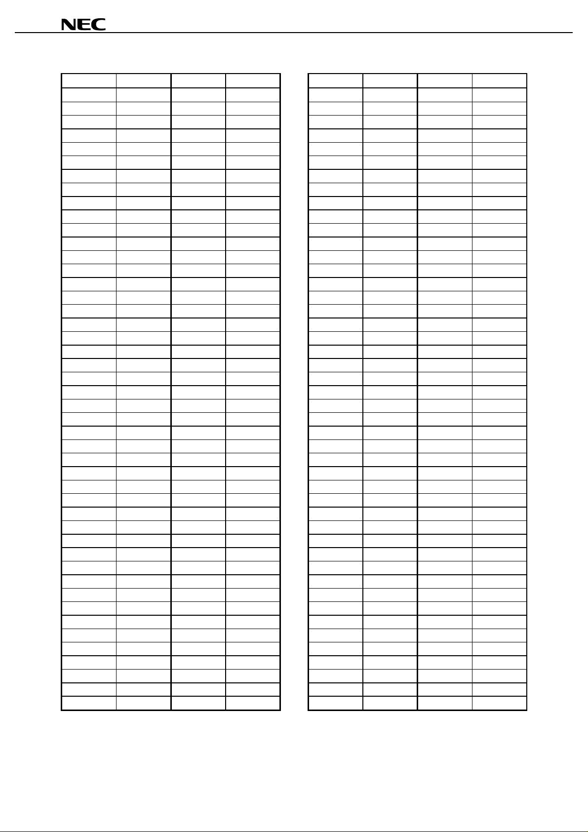
Module Pad Names
Pad Signal Name Pad Signal Name Pad Signal Name Pad Signal Name
A1 GND B1 GND A47 NC B47 NC
A2 LDQA8 B2 LDQA7 A48 NC B48 NC
A3 GND B3 GND A49 NC B49 NC
A4 LDQA6 B4 LDQA5 A50 NC B50 NC
A5 GND B5 GND A51 V
A6 LDQA4 B6 LDQA3 A52 GND B52 GND
A7 GND B7 GND A53 SCL B53 SA0
A8 LDQA2 B8 LDQA1 A54 V
A9 GND B9 GND A55 SDA B55 SA1
A10 LDQA0 B10 LCFM A56 SV
A11 GND B11 GND A57 SWP B57 SA2
A12 LCTMN B12 LCFMN A58 V
A13 GND B13 GND A59 RSCK B59 RCMD
A14 LCTM B14 NC A6 0 GND B60 GND
A15 GND B15 GND A61 RDQB7 B61 RDQB8
A16 NC B16 LROW2 A62 GND B62 GND
A17 GND B17 GND A63 RDQB5 B63 RDQB6
A18 LROW1 B18 LROW0 A64 GND B64 GND
A19 GND B19 GND A65 RDQB3 B65 RDQB4
A20 LCOL4 B20 LCOL3 A66 GND B66 GND
A21 GND B21 GND A67 RDQB1 B67 RDQB2
A22 LCOL2 B22 LCOL1 A68 GND B68 GND
A23 GND B23 GND A69 RCOL0 B69 RDQB0
A24 LCOL0 B24 LDQB0 A70 GND B70 GND
A25 GND B25 GND A71 RCOL2 B71 RCOL1
A26 LDQB1 B26 LDQB2 A72 GND B72 GND
A27 GND B27 GND A73 RCOL4 B73 RCOL3
A28 LDQB3 B28 LDQB4 A74 GND B74 GND
A29 GND B29 GND A75 RROW1 B75 RROW0
A30 LDQB5 B30 LDQB6 A76 GND B76 GND
A31 GND B31 GND A77 NC B77 RROW2
A32 LDQB7 B32 LDQB8 A78 GND B78 GND
A33 GND B33 GND A79 RCTM B79 NC
A34 LSCK B34 LCMD A80 GND B80 GND
A35 V
CMOS
B35 V
CMOS
A81 RCTMN B81 RCFMN
A36 SOUT B36 SIN A82 GND B82 GND
A37 V
CMOS
B37 V
CMOS
A83 RDQA0 B83 RCFM
A38 NC B38 NC A84 GND B84 GND
A39 GND B39 GND A85 RDQA2 B85 RDQA1
A40 NC B40 NC A86 GND B86 GND
A41 V
A42 V
DD
DD
B41 V
B42 V
DD
DD
A87 RDQA4 B87 RDQA3
A88 GND B88 GND
A43 NC B43 NC A89 RDQA6 B89 RDQA5
A44 NC B44 NC A90 GND B90 GND
A45 NC B45 NC A91 RDQA8 B91 RDQA7
A46 NC B46 NC A92 GND B92 GND
REF
DD
DD
B51 V
B54 V
DD
B56 SV
B58 V
REF
DD
DD
DD
4
Preliminary Data Sheet M14538EJ1V1DS00
MC-4R96CEE6B, 4R96CEE6C
Module Connector Pad Description (1/2)
Signal I/O Type Description
GND — — Ground reference for RDRAM core and interface. 72 PCB connector pads.
LCFM I RSL Clock from mas ter. Interface clock used for receiving RSL signals f rom the
Channel. Positive polarity.
LCFMN I RSL Clock from m as ter. Interface clock used for receiving RSL signals from the
Channel. Negative polarity.
LCMD I V
LCOL4..LCOL0 I RSL Column bus. 5-bit bus containing control and address information for column
LCTM I RSL Clock to master. Interface clock used for transmitting RS L s i gnal s to the
LCTMN I RSL Clock to mast er. Interface clock used for transmitting RS L signals to the
LDQA8..LDQA0 I/O RSL Data bus A. A 9-bit bus carrying a byte of read or write data between the Channel
LDQB8..LDQB0 I/O RSL Data bus B. A 9-bit bus carrying a byte of read or write data between the Channel
LROW2..LROW0 I RSL Row bus. 3-bit bus containing control and address information for row accesses.
LSCK I V
NC — — These pads are not connected. These 24 connec t or pads are reserved for future
RCFM I RSL Clock from master. Interfac e clock used for receiving RSL signals from the
RCFMN I RSL Clock from mas ter. Interface clock used for receiving RSL signals f rom the
RCMD I V
RCOL4..RCOL0 I RSL Column bus. 5-bit bus containi ng control and address information for column
RCTM I RSL Clock to master. Interface clock used for transmi t ting RSL signals to the
RCTMN I RSL Clock to master. Interface clock used for transmitting RS L s i gnal s to the
RDQA8..RDQA0 I/O RSL Data bus A. A 9-bit bus carrying a byte of read or write data between the Channel
RDQB8..RDQB0 I/O RSL Data bus B. A 9-bit bus carrying a byte of read or write data between the Channel
RROW2..RROW0 I RSL Row bus. 3-bit bus containing control and address informat i on for row accesses.
CMOS
CMOS
CMOS
Serial Command used t o read from and write to the control regis t ers. Also used
for power management.
accesses.
Channel. Positive polarity.
Channel. Negative polarity.
and the RDRAM. LDQA8 is non-functi onal on modules with x16 RDRAM devices.
and the RDRAM. LDQB8 is non-functi onal on modules with x16 RDRAM devices.
Serial clock input. Cl ock source used to read from and write t o the RDRAM
control registers.
use.
Channel. Positive polarity.
Channel. Negative polarity.
Serial Command Input used to read from and write to the control regi sters. Also
used for power management.
accesses.
Channel. Positive polarity.
Channel. Negative polarity.
and the RDRAM. RDQA8 is non-functi onal on modules with x16 RDRAM
devices.
and the RDRAM. RDQB8 is non-functi onal on modules with x16 RDRAM
devices.
Preliminary Data Sheet M14538EJ1V1DS00
5

MC-4R96CEE6B, 4R96CEE6C
Signal I/O Type Description
(2/2)
RSCK I V
SA0 I SV
SA1 I SV
SA2 I SV
SCL I SV
SDA I/O SV
SIN I/O V
SOUT I/O V
DD
SV
— — SPD Voltage. Us ed f or signals SCL, SDA, SWP, SA0, S A1 and SA2.
SWP I SV
CMOS
V
DD
V
REF
V
— — CMOS I/O Voltage. Used for signals CMD, SCK, SIN, SOUT.
— — Supply voltage for the RDRAM c ore and i n t e rf ace logic.
— — Logic threshold referenc e vol tage for RSL signals.
CMOS
DD
DD
DD
DD
DD
CMOS
CMOS
DD
Serial clock input. Cl ock source used to read from and write t o the RDRAM
control registers.
Serial Presence Detect Address 0.
Serial Presence Detect Address 1.
Serial Presence Detect Address 2.
Serial Presence Detec t Clock.
Serial Presence Detect Data (Open Collector I/O).
Serial I/O for reading from and writing to the control registers. Attaches to SIO0
of the first RDRAM on the module.
Serial I/O for reading from and writing to the control registers. Attaches to SIO1
of the last RDRAM on the modul e.
Serial Presence Detect Write Protect (active high). W hen l ow, t he S PD can be
written as well as read.
6
Preliminary Data Sheet M14538EJ1V1DS00

Block Diagram
V
REF
LCMD
LSCK
SIN
LDQB 7
LDQB 8
DQB 7
DQB 8
SIO 0
SIO 1
SCK
CMD
REF
V
DQB 7
DQB 8
SIO 0
SIO 1
SCK
CMD
REF
V
LDQB 5
LDQB 6
DQB 5
DQB 6
DQB 5
DQB 6
LDQB 3
LDQB 4
DQB 3
DQB 4
DQB 3
DQB 4
LDQB 1
LDQB 2
DQB 1
DQB 2
DQB 1
DQB 2
LDQB 0
LCOL 0
COL 0
DQB 0
COL 0
DQB 0
LCOL 2
LCOL 1
COL 2
COL 1
COL 2
COL 1
LCOL 4
LCOL 3
COL 4
COL 3
COL 4
COL 3
LROW 1
LROW 0
ROW 1
ROW 0
U1
ROW 1
ROW 0
U2
MC-4R96CEE6B, 4R96CEE6C
LROW 2
LCTMN
CTMN
ROW 2
CTMN
ROW 2
LCTM
CTM
CTM
LCFMN
LCFM
CFM
CFMN
CFM
CFMN
LDQA 1
LDQA 0
DQA 1
DQA 0
DQA 1
DQA 0
LDQA 3
LDQA 2
DQA 3
DQA 2
DQA 3
DQA 2
LDQA 4
DQA 4
DQA 4
LDQA 6
LDQA 5
DQA 6
DQA 5
DQA 6
DQA 5
LDQA 8
LDQA 7
DQA 8
DQA 7
DQA 8
DQA 7
V
CMOS
V
DD
SCL
SWP
47 kΩ
RCMD
SCL
WP
A0
SA0
SOUT
RSCK
SV
DD
V
CC
U0
A1 A2
SA1 SA2
DQB 8
SIO 0
SIO 1
SCK
CMD
REF
V
DQB 8
SIO 0
SIO 1
SCK
CMD
REF
V
RDQB 8
SDA
DQB 5
DQB 6
DQB 7
DQB 5
DQB 6
DQB 7
RDQB 5
RDQB 6
RDQB 7
SERIAL PD
DQB 3
DQB 4
DQB 3
DQB 4
RDQB 3
RDQB 4
SDA
DQB 1
DQB 2
DQB 1
DQB 2
RDQB 1
RDQB 2
SV
DD
COL 0
DQB 0
COL 0
DQB 0
RCOL 0
RDQB 0
COL 2
COL 1
COL 2
COL 1
RCOL 2
RCOL 1
0.1 µF
COL 4
COL 3
COL 4
COL 3
RCOL 4
RCOL 3
ROW 1
ROW 0
U3
ROW 1
ROW 0
U6
RROW 1
RROW 0
V
CTMN
ROW 2
CTMN
ROW 2
RCTMN
RROW 2
V
DD
CMOS
CFMN
CTM
CFMN
CTM
RCFMN
RCTM
DQA 1
DQA 0
CFM
DQA 1
DQA 0
CFM
RDQA 1
RDQA 0
RCFM
2 per
RDRAM
0.1 µF
1 per
2 RDRAMs
0.1 µF
DQA 3
DQA 2
DQA 3
DQA 2
RDQA 3
RDQA 2
DQA 5
DQA 4
DQA 5
DQA 4
RDQA 5
RDQA 4
V
REF
DQA 7
DQA 6
DQA 7
DQA 6
RDQA 7
RDQA 6
DQA 8
DQA 8
RDQA 8
1 per
2 RDRAMs
Plus one
Near Connector
0.1 µF
Remarks 1.
Rambus Channel signals form a loop through the RIMM module, with the exception of the SIO chain.
2.
See Serial Presence Detection Specification for information on the SPD device and its contents.
Preliminary Data Sheet M14538EJ1V1DS00
7

MC-4R96CEE6B, 4R96CEE6C
Electrical Specification
Absolute Maximum Ratings
Symbol Parameter MIN. MAX. Unit
I,ABS
V
DD,ABS
V
STORE
T
Caution Exposing the device to stress above those listed in Absolute Maximum Ratings could cause
DC Recommended Electrical Conditions
Symbol Parameter and conditions MIN. MAX. Unit
DD
V
CMOS
V
REF
V
IL
V
IH
V
IL,CMOS
V
IH,CMOS
V
OL,CMOS
V
OH,CMOS
V
REF
I
SCK,CMD
I
SIN,SOUT
I
Voltage applied to any RSL or CMOS signal pad with respect to GND
Voltage on VDD with respect to GND
Storage temperature
0.3 VDD + 0.3 V
−
0.5 VDD + 1.0 V
−
50 +100 °C
−
permanent damage. The device is not meant to be operated under conditions outside the limits
described in the operational section of this specification. Exposure to Absolute Maximum Rating
conditions for extended periods may affect device reliability.
Supply voltage 2.50 − 0.13 2.50 + 0.13 V
CMOS I/O power supply at pad 2.5V controllers 2.5 − 0.13 2. 5 + 0. 25 V
1.8V controllers 1.8 − 0.1 1.8 + 0.2
Reference voltage 1.4 − 0.2 1.4 + 0.2 V
RSL input low voltage V
RSL input high voltage V
CMOS input low voltage
CMOS input high voltage 0.5V
CMOS output low voltage, I
CMOS output high voltage, I
REF
V
current, V
REF,MAX
CMOS input leakage current, (0 ≤ V
CMOS input leakage current, (0 ≤ V
OL,CMOS
= 1 mA
OH,CMOS
= −0.25 mA V
CMOS
≤ VDD)
CMOS
≤ VDD)
REF
− 0.5 V
REF
+ 0.2 V
0.3 0.5V
−
CMOS
+0.25 V
—
CMOS
− 0.3
60.0 +60.0
−
60.0 +60.0 µA
−
10.0 +10.0 µA
−
REF
− 0.2 V
REF
+ 0.5 V
CMOS
− 0.25 V
CMOS
+ 0.3 V
0.3 V
—
V
A
µ
8
Preliminary Data Sheet M14538EJ1V1DS00

AC Electrical Specifications
MC-4R96CEE6B, 4R96CEE6C
Symbol
Z Module Impedance
PD
T
Average clock delay f rom finger to finger of all RSL clock nets -845 1.40 ns
(CTM, CTMN,CFM, and CFMN) -745 1.40
T
∆
T
∆
PD
PD-CMOS
Propagation delay variation of RSL si gnal s with respect to TPD
Propagation delay variation of SCK and CMD si gnal s with respect to
an average clock delay
Attenuation Limit -845 14 %
IN
Vα/V
Forward crosstalk coefficient -845 3 %
IN
VXF/V
(300ps input rise time 20% - 80%) -745 3
VXB/V
IN
Backward
crosstalk coefficient -845 1.8 %
(300ps input rise time 20% - 80%) -745 1.8
R
DC
DC Resistance Limit -845 0.7
Parameter and Conditions MIN.
25.2 28 30.8
-653 1.40
Note1
Note1,2
21 +21 ps
−
100 +100 ps
−
-745 14
-653 9
-653 3
-653 1.8
-745 0.7
-653 0.7
TYP. MAX. Unit
Ω
Ω
Notes 1.
PD
T
or Average clock delay is defined as the average delay from finger to finger of all RSL clock nets (CTM,
CTMN, CFM, and CFMN).
2.
If the RIMM module meets the following specification, then it is compliant to the specification.
If the RIMM module does not meet these specifications, then the specification can be adjusted by the
PD
Specification” table.
Adjusted
“Adjusted ∆T
PD
Specification
T
∆∆∆∆
Symbol Parameter and conditions Adjusted MIN./MAX. Absolute Unit
MIN. MAX.
PD
Propagation delay variation of RSL si gnal s with respect to T
T
∆
Note
N = Number of RDRAM devices installed on the RIMM module.
∆Z0 = delta Z0% = (MAX. Z0
− MIN. Z0) / (MIN. Z0)
+/− [17+(18*N*∆Z0)]
PD
Note
30 +30 ps
−
(MAX. Z0 and MIN. Z0 are obtained from the loaded (high impedance) impedance coupons of all RSL layers
on the module.)
Preliminary Data Sheet M14538EJ1V1DS00
9

RIMM Module Current Profile
DD
I
DD1
I
DD2
I
DD3
I
DD4
I
DD5
I
DD6
I
One RDRAM in Read , balance in NAP mode
One RDRAM in Read , balance in Standby mode
One RDRAM in Read , balance in Active mode
One RDRAM in Write, bal anc e i n NAP mode
One RDRAM in Write, bal anc e i n Standby mode
One RDRAM in Write, bal anc e i n Active mode
RIMM module power conditions
MC-4R96CEE6B, 4R96CEE6C
MAX. Unit
TBD mA
TBD mA
TBD mA
TBD mA
TBD mA
TBD mA
10
Preliminary Data Sheet M14538EJ1V1DS00

MC-4R96CEE6B, 4R96CEE6C
Timing Parameters
The following timing parameters are from the RDRAMs pins, not the RIMM. Please refer to the RDRAM data sheet
(
µ
PD488448, 488488) for detailed timing diagrams.
Para- Description MIN. MAX. Units
meter -845 -745 -653
t
RC
t
RAS
t
RP
t
PP
t
RR
t
RCD
t
CAC
t
CWD
t
CC
t
PACKET
t
RTR
t
OFFP
t
RDP
t
RTP
Row Cycle time of RDRAM banks - the interval between ROWA packets with
28 28 28 — t
ACT commands to the same bank.
RAS-asserted time of RDRAM bank - the interval between ROWA packet with ACT
command and next ROWR packet with PRER
Note 1
command to the same bank.
Row Precharge time of RDRAM banks - the interval between ROWR packet with
Note 1
PRER
command and next ROWA packet with ACT command to the same
20 20 20
888—t
Note 2
64µs
bank.
Precharge-to-precharge time of RDRAM device - the interval between
successive ROWR packets with PRER
Note 1
commands to any banks of the
888—t
same device.
RAS-to-RAS time of RDRAM device - the interval between successive ROWA
888—t
packets with ACT com m ands to any banks of the same device.
RAS-to-CAS Delay - the int erval from ROWA packet with ACT command to
977—t
COLC packet with RD or WR comm and. Note - the RAS-to-CAS delay seen
by the RDRAM core (t
) is equal to t
RCD-C
RCD-C = 1 + tRCD
because of differences
in the row and column paths through the RDRAM interface.
CAS Access delay - the interval from RD command t o Q read data. The
equation for t
is given in the TPARM register.
CAC
88812t
CAS Write Delay - interval from WR command to D writ e data. 6 6 6 6 t
CAS-to-CAS time of RDRAM bank - the interval between successive COLC
444—t
commands.
Length of ROWA, ROWR, COLC, COLM or COLX pac ket. 4 4 4 4 t
Interval from COLC packet wi th WR command to COLC packet whic h c auses
888—t
retire, and to COLM packet with bytemask.
The interval (offset) f rom COLC packet with RDA command, or from COLC
4444t
packet with retire command (after WRA automatic prec harge), or from COLC
packet with PREC comm and, or from COLX packet with P RE X command to
the equivalent ROWR packet with PRER. The equation for t
is given in the
OFFP
TPARM register.
Interval from last COLC packet with RD comm and to ROWR packet with
444—t
PRER.
Interval from last COLC packet with automatic retire command to ROWR
444—t
packet with PRER.
CYCLE
t
CYCLE
CYCLE
CYCLE
CYCLE
CYCLE
CYCLE
CYCLE
CYCLE
CYCLE
CYCLE
CYCLE
CYCLE
CYCLE
Notes 1.
Or equivalent PREC or PREX command.
This is a constraint imposed by the core, and is therefore in units of ms rather than t
2.
Preliminary Data Sheet M14538EJ1V1DS00
CYCLE
.
11

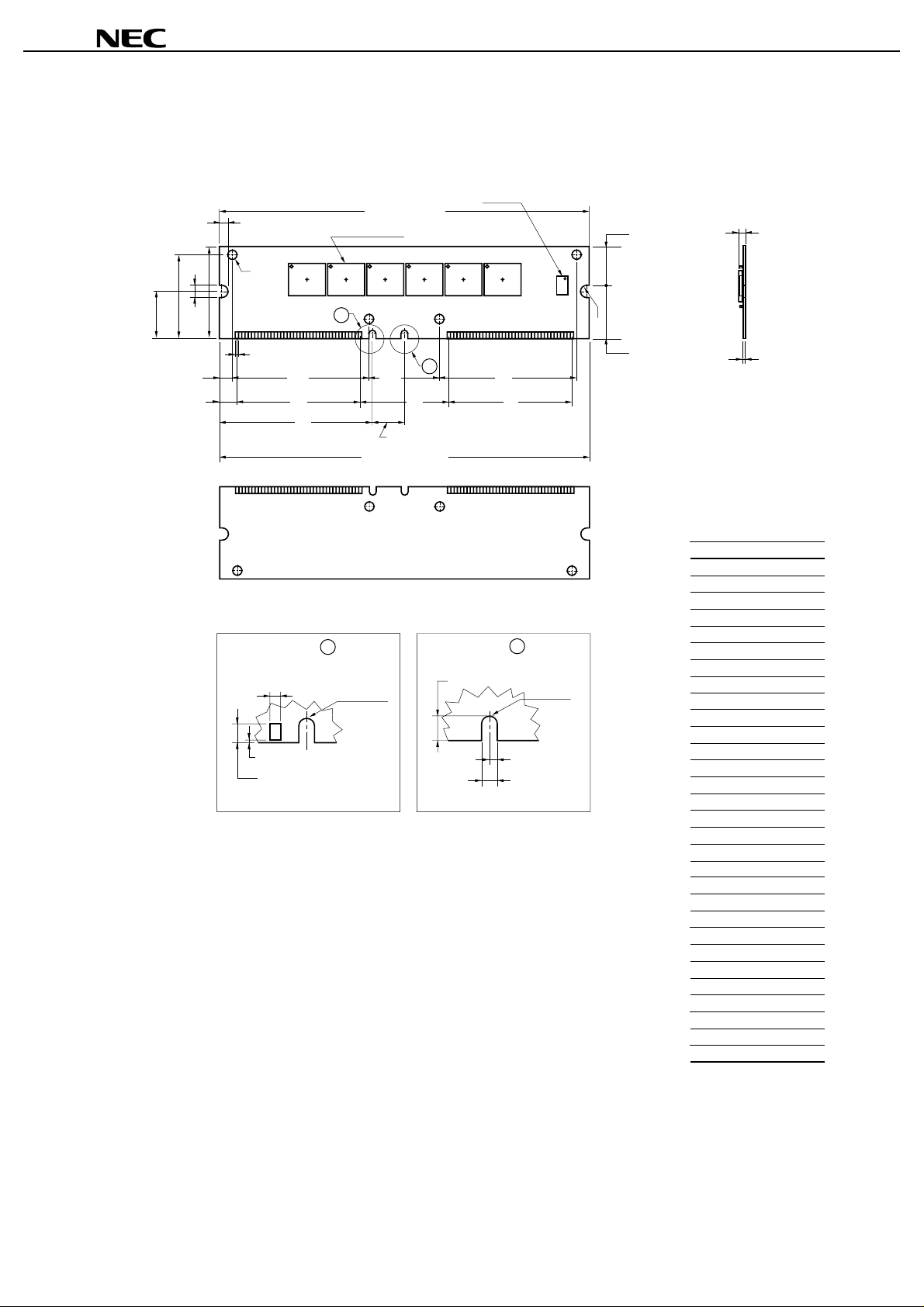
Package Drawings
[MC-4R96CEE6B]
184 EDGE CONNECTOR PADS RIMM (SOCKET TYPE)
EEPROM
R
A (AREA B)
128 M Direct RDRAM
MC-4R96CEE6B, 4R96CEE6C
M1 (AREA B)
V
P
ON M
K
G
S
L
H
B
detail of A part
W
Y
X
A
A1 (AREA A)
R1.00
Q
B
I
J
M2 (AREA A)
T
FDE
C
ITEM MILLIMETERS
133.35 TYP.
A
133.35±0.13
A1
55.175
B
1.00±0.10
B1
11.50
detail of B part
C1
B1
Z
R1.00
C
C1
D
E
F
G
H
I
J
K
L
M
M1
M2
N
O
P
Q
R
S
T
V
W
X
Y
Z
3.00±0.10
45.00
32.00
45.00
5.675
47.625
25.40
47.625
6.35
1.00 TYP.
31.75±0.13
11.97
19.78
29.21
17.78
4.00±0.10
R 2.00
3.00±0.10
φ
2.44
1.27±0.10
2.24 MAX.
0.80±0.10
2.99
0.15
2.00±0.10
12
Preliminary Data Sheet M14538EJ1V1DS00
[MC-4R96CEE6C]
184 EDGE CONNECTOR PADS RIMM (SOCKET TYPE)
EEPROM
R
A (AREA B)
128 M Direct RDRAM
MC-4R96CEE6B, 4R96CEE6C
M1 (AREA B)
V
P
ON M
K
G
S
L
H
B
detail of A part
W
Y
X
A
A1 (AREA A)
R1.00
Q
B
I
J
M2 (AREA A)
T
FDE
C
ITEM MILLIMETERS
133.35 TYP.
A
133.35±0.13
A1
55.175
B
1.00±0.10
B1
11.50
detail of B part
C1
B1
Z
R1.00
C
C1
D
E
F
G
H
I
J
K
L
M
M1
M2
N
O
P
Q
R
S
T
V
W
X
Y
Z
3.00±0.10
45.00
32.00
45.00
5.675
47.625
25.40
47.625
6.35
1.00 TYP.
31.75±0.13
11.97
19.78
29.21
17.78
4.00±0.10
R 2.00
3.00±0.10
φ
2.44
1.27±0.10
2.43 MAX.
0.80±0.10
2.99
0.15
2.00±0.10
Preliminary Data Sheet M14538EJ1V1DS00
13

[MC-4R96CEE6B, MC-4R96CEE6C]
★
184 EDGE CONNECTOR PADS RIMM (SOCKET TYPE)
A
MC-4R96CEE6B, 4R96CEE6C
B
E
Pad A1 Pad A92
C C
D
ITEM
A
B
C
D
E
F
G
H
DESCRIPTION
PCB length
PCB height for 1.25" RIMM Module
Center-center pad width from pad A1 to A46,
A47 to A92, B1 to B46 or B47 to B92
Spacing from PCB left edge to connector key notch
Spacing from contact pad PCB edge
to side edge retainer notch
PCB thickness
Heat spreader thickness from PCB surface (one side) to
heat spreader top surface
RIMM thickness
MIN.
133.22
31.62
44.95
-
-
1.17
-
-
TYP.
133.35
31.75
45.00
55.175
17.78
1.27
-
-
MAX.
133.48
31.88
45.05
-
-
1.37
3.09
4.46
G
F
H
UNIT
mm
mm
mm
mm
mm
mm
mm
mm
14
Preliminary Data Sheet M14538EJ1V1DS00

MC-4R96CEE6B, 4R96CEE6C
NOTES FOR CMOS DEVICES
1 PRECAUTION AGAINST ESD FOR SEMICONDUCTORS
Note:
Strong electric field, when exposed to a MOS device, can cause destruction of the gate oxide and
ultimately degrade the device operation. Steps must be taken to stop generation of static electricity
as much as possible, and quickly dissipate it once, when it has occurred. Environmental control
must be adequate. When it is dry, humidifier should be used. It is recommended to avoid using
insulators that easily build static electricity. Semiconductor devices must be stored and transported
in an anti-static container, static shielding bag or conductive material. All test and measurement
tools including work bench and floor should be grounded. The operator should be grounded using
wrist strap. Semiconductor devices must not be touched with bare hands. Similar precautions need
to be taken for PW boards with semiconductor devices on it.
2 HANDLING OF UNUSED INPUT PINS FOR CMOS
Note:
No connection for CMOS device inputs can be cause of malfunction. If no connection is provided
to the input pins, it is possible that an internal input level may be generated due to noise, etc., hence
causing malfunction. CMOS devices behave differently than Bipolar or NMOS devices. Input levels
of CMOS devices must be fixed high or low by using a pull-up or pull-down circuitry. Each unused
DD
pin should be connected to V
being an output pin. All handling related to the unused pins must be judged device by device and
related specifications governing the devices.
or GND with a resistor, if it is considered to have a possibility of
3 STATUS BEFORE INITIALIZATION OF MOS DEVICES
Note:
Power-on does not necessarily define initial status of MOS device. Production process of MOS
does not define the initial operation status of the device. Immediately after the power source is
turned ON, the devices with reset function have not yet been initialized. Hence, power-on does
not guarantee out-pin levels, I/O settings or contents of registers. Device is not initialized until the
reset signal is received. Reset operation must be executed immediately after power-on for devices
having reset function.
Preliminary Data Sheet M14538EJ1V1DS00
15

MC-4R96CEE6B, 4R96CEE6C
Rambus, RDRAM and the Rambus Logo are registered trademarks of Rambus Inc.
DirectRambus, DirectRDRAM, RIMM, RModule and RSocket are trademarks of Rambus Inc.
BGA is a registered trademark of Tessera Inc.
µµµµ
D2BGA is a trademark of NEC Corporation.
CAUTION FOR HANDLING MEMORY MODULES
When handling or inserting memory modules, be sure not to touch any components on the modules, such as
the memory IC, chip capacitors and chip resistors. It is necessary to avoid undue mechanical stress on these
components to prevent damaging them.
When re-packing memory modules, be sure the modules are NOT touching each other. Modules in contact
with other modules may cause excessive mechanical stress, which may damage the modules.
• The information in this document is subject to change without notice. Before using this document, please
confirm that this is the latest version.
• No part of this document may be copied or reproduced in any form or by any means without the prior written
consent of NEC Corporation. NEC Corporation assumes no responsibility for any errors which may appear in
this document.
• NEC Corporation does not assume any liability for infringement of patents, copyrights or other intellectual property
rights of third parties by or arising from use of a device described herein or any other liability arising from use
of such device. No license, either express, implied or otherwise, is granted under any patents, copyrights or other
intellectual property rights of NEC Corporation or others.
• Descriptions of circuits, software, and other related information in this document are provided for illustrative
purposes in semiconductor product operation and application examples. The incorporation of these circuits,
software, and information in the design of the customer's equipment shall be done under the full responsibility
of the customer. NEC Corporation assumes no responsibility for any losses incurred by the customer or third
parties arising from the use of these circuits, software, and information.
• While NEC Corporation has been making continuous effort to enhance the reliability of its semiconductor devices,
the possibility of defects cannot be eliminated entirely. To minimize risks of damage or injury to persons or
property arising from a defect in an NEC semiconductor device, customers must incorporate sufficient safety
measures in its design, such as redundancy, fire-containment, and anti-failure features.
• NEC devices are classified into the following three quality grades:
"Standard", "Special", and "Specific". The Specific quality grade applies only to devices developed based on a
customer designated "quality assurance program" for a specific application. The recommended applications of
a device depend on its quality grade, as indicated below. Customers must check the quality grade of each device
before using it in a particular application.
Standard: Computers, office equipment, communications equipment, test and measurement equipment,
audio and visual equipment, home electronic appliances, machine tools, personal electronic
equipment and industrial robots
Special: Transportation equipment (automobiles, trains, ships, etc.), traffic control systems, anti-disaster
systems, anti-crime systems, safety equipment and medical equipment (not specifically designed
for life support)
Specific: Aircraft, aerospace equipment, submersible repeaters, nuclear reactor control systems, life
support systems or medical equipment for life support, etc.
The quality grade of NEC devices is "Standard" unless otherwise specified in NEC's Data Sheets or Data Books.
If customers intend to use NEC devices for applications other than those specified for Standard quality grade,
they should contact an NEC sales representative in advance.
M7 98. 8
 Loading...