

Page 1

PART NO. 599910588
•
SERVICE MANUAL
COLOR MONITOR
MultiSync
LCD1550V
MODELS LCD1550V-1 (B)/-BK(B)
This model changed a LCD panel (manufactured by Hannstar) from the original model.
Use the applicable service manual which surely confirms the model number of the
NAME PLATE, INSTRUCTION.
Refer to the page which the point of view of the model number is mentioned in.
• Model number : LA-15R02 / LA-15R02-BK
Maintenance is performed by the original service manual (Part No.
599910571).
Model number : LA-15R02-1 / LA-15R02-1-BK
Maintenance is performed using this service manual.
NEC-MITSUBISHI ELECTRIC VISUAL SYSTEMS CORPORATION
JUNE 2002
200206
08109741
08109742
Page 2
The SERVICE PERSONNEL should have the appropriate technical training, knowledge and experience
necessary to:
• Be familiar with specialized test equipment, and
• Be careful to follow all safety procedures to minimize danger to themselves and their coworkers.
To avoid electrical shocks, this equipment should be used with an appropriate power cord.
This equipment utilized a micro-gap power switch. Turn off the set by first pushing power switch. Next,
remove the power cord from the AC outlet.
To prevent fire or shock hazards, do not expose this unit to rain or moisture.
This symbol warns the personnel that un-insulated voltage within the unit may have sufficient
magnitude to cause electric shock.
This symbol alerts the personnel that important literature concerning the operation and
maintenance of this unit has been included.
Therefore, it should be read carefully in order to avoid any problems.
WARNING
PRODUCT SAFETY CAUTION
1. When parts replacement is required for servicing, always use the manufacturer's specified replacement.
2. When replacing the component, always be certain that all the components are put back in the place.
3. As for a connector, pick and extract housing with fingers properly since a disconnection and improper
contacts may occur, when wires of the connector are led.
4. Use a proper screwdriver. If you use screwdriver that does not fit, you may damage the screws.
Page 3
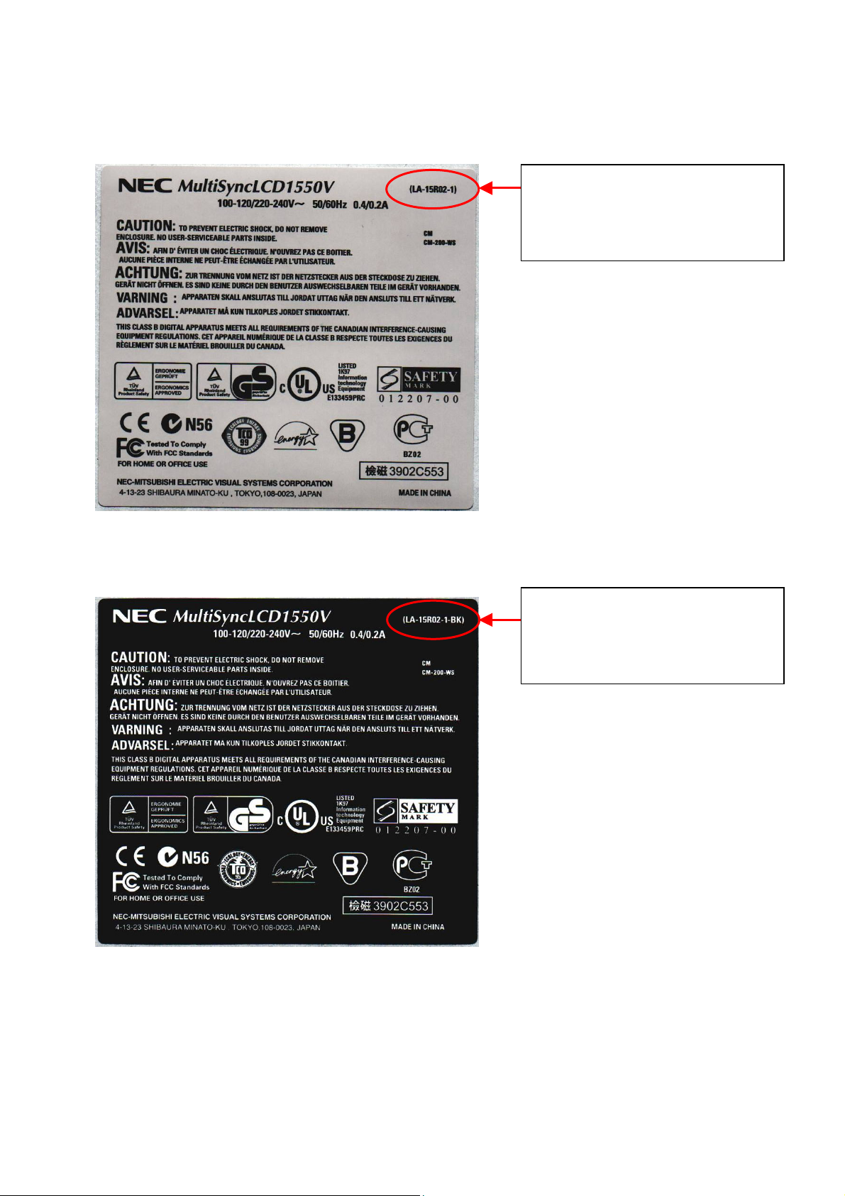
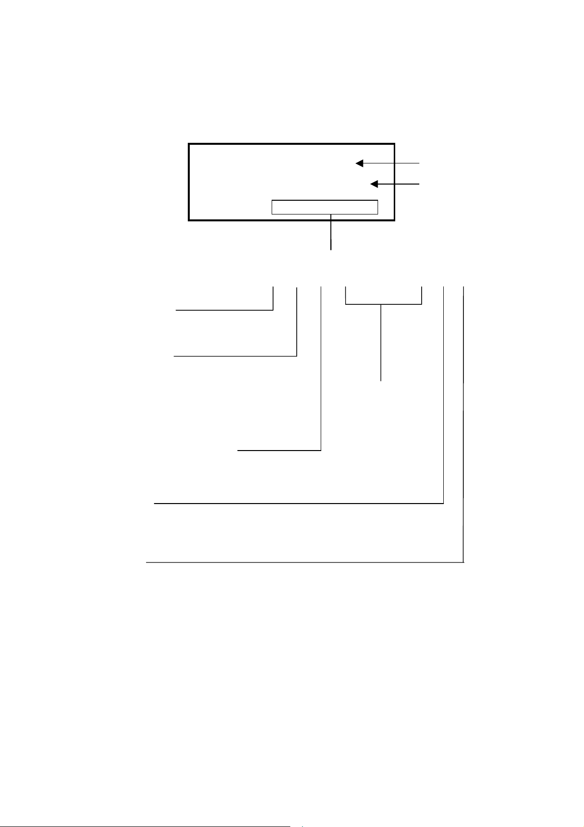
Point of view of the model number
NAME PLATE, INSTRUCTION (White model)
NAME PLATE, INSTRUCTION (Black model)
Model number
Original model: LA-15R02
Hannstar LCD model: LA-15R02-1
Model number
Original model: LA-15R02-BK
Hannstar LCD model: LA-15R02-1-BK
Page 4

CONTENTS
USER'S MANUAL ------------------------------------------------------------------- 1-1
SERIAL NUMBER INFORMATION --------------------------------------------- 2-1
DISASSEMBLY ----------------------------------------------------------------------- 3-1
ADJUSTMENT PROCEDURES -------------------------------------------------- 4-1
INSPECTION --------------------------------------------------------------------------- 5-1
TROUBLE SHOOTING ------------------------------------------------------------- 6-1
CIRCUIT DESCRIPTION ----------------------------------------------------------- 7-1
Page No.
REPLACEMENT PARTS LIST --------------------------------------------------- 8-1
BLOCK DIAGRAM ------------------------------------------------------------------- 9-1
SCHEMATIC DIAGRAMS -------------------------------------------------------- 10-1
Page 5

USER'S MANUAL
MultiSync LCD1550V
User’s Manual
UÏivatelská pfiíruãka
Bedienerhandbuch
Οδηγίες Χρήσης
Manual del usuario
Manuel Utilisateur
Manuale utente
Gebruikershandleiding
Podr´cznik u˝ytkownika
Руководство пользователя
Kullan∂c∂ Klavuzu
1-1
Page 6
Declaration
Declaration of the Manufacturer
We hereby certify that the colour monitor
MultiSync LCD1550V (LA-15R02)
MultiSync LCD1550V (LA-15R02-BK)
MultiSync LCD1550V (LA-15R02-1)
MultiSync LCD1550V (LA-15R02-1-BK)
is in compliance with
Council Directive 73/23/EEC:
Council Directive 89/336/EEC:
and marked with
– EN 60950
– EN 55022
– EN 61000-3-2
– EN 61000-3-3
– EN 55024
NEC-Mitsubishi Electric Visual Systems, Corp.
MS Shibaura Bldg., 13-23,
Shibaura 4-chome,
Minato-Ku, Tokyo 108-0023, Japan
1-2
Page 7

TCO’99
This is a translation of the original English TCO'99 document.
MultiSync LCD1550V White Model (LA-15R02 and LA-15R02-1)
Congratulations! You have just purchased a TCO’99
approved and labeled product! Your choice has
provided you with a product developed for
professional use. Your purchase has also contributed
to reducing the burden on the environment and also
to the further development of environmentally
adapted electronics products.
Why do we have environmentally labelled computers?
In many countries, environmental labelling has become an established
method for encouraging the adaptation of goods and services to the
environment. The main problem, as far as computers and other
electronics equipment are concerned, is that environmentally harmful
substances are used both in the products and during the manufacturing.
Since it has not been possible for the majority of electronics equipment
to be recycled in a satisfactory way, most of these potentially damaging
substances sooner or later enter Nature.
There are also other characteristics of a computer, such as energy
consumption levels, that are important from the viewpoints of both the
work (Internal) and natural (external) environments. Since all methods of
conventional electricity generation have a negative effect on the
environment (acidic and climate-influencing emissions, radioactive
waste, etc.), it is vital to conserve energy. Electronics equipment in
offices consume an enormous amount of energy since they are often left
running continuously.
What does labelling involve?
This product meets the requirements for the TCO’99 scheme which
provides for international and environmental labelling of personal
computers. The labelling scheme was developed as a joint effort by the
TCO (The Swedish Confederation of Professional Employees), Svenska
Naturskyddsforeningen (The Swedish Society for Nature Conservation)
and Statens Energimyndighet (The Swedish National Energy
Administration).
1-3
Page 8

The requirements cover a wide range of issues: environment,
ergonomics, usability, emission of electrical and magnetic fields, energy
consumption and electrical and fire safety.
The environmental demands concern restrictions on the presence and
use of heavy metals, brominated and chlorinated flame retardants,
CFCs (freons) and chlorinated solvents, among other things. The
product must be prepared for recycling and the manufacturer is obliged
to have an environmental plan which must be adhered to in each
country where the company implements its operational policy. The
energy requirements include a demand that the computer and/or
display, after a certain period of inactivity, shall reduce its power
consumption to a lower level in one or more stages. The length of time
to reactivate the computer shall be reasonable for the user.
Labelled products must meet strict environmental demands, for
example, in respect of the reduction of electric and magnetic fields,
physical and visual ergonomics and good usability.
Environmental Requirements
Flame retardants
Flame retardants are present in printed circuit boards, cables, wires,
casings and housings. In turn, they delay the spread of fire. Up to thirty
percent of the plastic in a computer casing can consist of flame
retardant substances. Most flame retardants contain bromine or chloride
and these are related to another group of environmental toxins, PCBs,
which are suspected to give rise to severe health effects, including
reproductive damage in fisheating birds and mammals, due to the
bioaccumulative* processes. Flame retardants have been found in
human blood and researchers fear that disturbances in foetus
development may occur.
TCO’99 demand requires that plastic components weighing more than
25 grams must not contain flame retardants with organically bound
chlorine and bromine. Flame retardants are allowed in the printed circuit
boards since no substitutes are available.
Lead**
Lead can be found in picture tubes, display screens, solders and
capacitors. Lead damages the nervous system and in higher doses,
causes lead poisoning.
TCO’99 requirement permits the inclusion of lead since no replacement
has yet been developed.
1-4
Page 9

Cadmium**
Cadmium is present in rechargeable batteries and in the
colourgenerating layers of certain computer displays. Cadmium
damages the nervous system and is toxic in high doses.
TCO’99 requirement states that batteries, the colourgenerating layers of
display screens and the electrical or electronics components must not
contain any cadmium.
Mercury**
Mercury is sometimes found in batteries, relays and switches, Mercury
damages the nervous system and is toxic in high doses.
TCO’99 requirement states that batteries may not contain any Mercury.
It also demands that no mercury is present in any of the electrical or
electronics components associated with the display unit.
CFCs (freons)
CFCs (freons) are sometimes used for washing printed circuit boards.
CFCs break down ozone and thereby damage the ozone layer in the
stratosphere, causing increased reception on Earth of ultraviolet light
with consequent increased risks of skin cancer (malignant melanoma).
The relevant TCO’99 requirement; Neither CFCs nor HCFCs may be
used during the manufacturing and assembly of the product or its
packaging.
* Bio-accumulative is defined as substances which accumulate within
living organisms.
** Lead, Cadmium and Mercury are heavy metals which are
Bioaccumulative.
To obtain complete information on the environmental criteria document,
order from:
TCO Development Unit
SE-114 94 Stockholm
SWEDEN
FAX Number: +46 8 782 92 07
E-mail (Internet): development@tco.se
You may also obtain current information on TCO’99 approved and
labelled products by visiting their website at:
http://www.tco-info.com/
1-5
Page 10

TCO’95
This is a translation of the original English TCO'95 document.
MultiSync LCD1550V Black Model (LA-15R02-BK and LA-15R02-1-BK)
Congratulations! You have just purchased a TCO’95
approved and labeled product! Your choice has
provided you with a product developed for
professional use. Your purchase has also
contributed to reducing the burden on the
environment and also, to the further development of
environmentally adapted electronics products.
Why do we have environmentally labelled computers?
In many countries, environmental labelling has become an established
method for encouraging the adaptation of goods and services to the
environment. The main problem, as far as computers and other
electronics equipment are concerned, is that environmentally harmful
substances are used both in the products and during the manufacturing.
Since it has not been possible for the majority of electronics equipment
to be recycled in a satisfactory way, most of these potentially damaging
substances sooner or later enter Nature.
There are also other characteristics of a computer, such as energy
consumption levels, that are important from the viewpoints of both the
work (Internal) and natural (external) environments. Since all methods of
conventional electricity generation have a negative effect on the
environment (acidic and climate-influencing emissions, radioactive
waste, etc.), it is vital to conserve energy. Electronics equipment in
offices consume an enormous amount of energy since they are often left
running continuously.
What does labelling involve?
This product meets the requirements for the TCO’95 scheme which
provides for international and environmental labelling of personal
computers. The labelling scheme was developed as a joint effort by the
TCO (The Swedish Confederation of Professional Employees),
Naturskyddsforeningen (The Swedish Society for Nature Conservation)
and NUTEK (The National Board for Industrial and Technical
Development in Sweden).
The requirements cover a wide range of issues: environment,
ergonomics, usability, emission of electrical and magnetic fields, energy
consumption and electrical and fire safety.
1-6
Page 11

The environmental demands concern restrictions on the presence and
use of heavy metals, brominated and chlorinated flame retardants,
CFCs (freons) and chlorinated solvents, among other things. The
product must be prepared for recycling and the manufacturer is obliged
to have an environmental plan which must be adhered to in each
country where the company implements its operational policy. The
energy requirements include a demand that the computer and/or
display, after a certain period of inactivity, shall reduce its power
consumption to a lower level in one or more stages. The length of time
to reactivate the computer shall be reasonable for the user.
Labelled products must meet strict environmental demands, for
example, in respect of the reduction of electric and magnetic fields,
physical and visual ergonomics and good usability.
TCO’95 is a co-operative project between TCO (The Swedish
Confederation of Professional Employees), Naturskyddsforeningen
(The Swedish Society for Nature Conservation) and NUTEK
(The National Board for Industrial and Technical Development in
Sweden).
Environmental Requirements
Brominated flame retardants
Brominated flame retardants are present in printed circuit boards,
cables, wires, casings and housings. In turn, they delay the spread of
fire. Up to thirty percent of the plastic in a computer casing can consist
of flame retardant substances. These are related to another group of
environmental toxins, PCBs, which are suspected to give rise to similar
harm, including reproductive damage in fisheating birds and mammals,
due to the bio-accumulative* processes. Flame retardants have been
found in human blood and researchers fear that disturbances in foetus
development may occur.
TCO’95 demand requires that plastic components weighing more than
25 grams must not contain organically bound chlorine and bromine.
Lead**
Lead can be found in picture tubes, display screens, solders and
capacitors. Lead damages the nervous system and in higher doses,
causes lead poisoning.
TCO’95 requirement permits the inclusion of lead since no replacement
has yet been developed.
1-7
Page 12

Cadmium**
Cadmium is present in rechargeable batteries and in the
colourgenerating layers of certain computer displays. Cadmium
damages the nervous system and is toxic in high doses.
TCO’95 requirement states that batteries may not contain more than
25 ppm (parts per million) of cadmium. The colourgenerating layers of
display screens must not contain any cadmium.
Mercury**
Mercury is sometimes found in batteries, relays, switches, and back-light
systems, Mercury damages the nervous system and is toxic in high
doses.
TCO’95 requirement states that batteries may not contain more than
25 ppm (parts per million) of mercury. It also demands that no mercury
is present in any of the electrical or electronics components concerned
with the display unit, except the back-light system.
CFCs (freons)
CFCs (freons) are sometimes used for washing printed circuit boards
and in the manufacturing of expanded foam for packaging. CFCs break
down ozone and thereby damage the ozone layer in the stratosphere,
causing increased reception on Earth of ultraviolet light with consequent
increased risks of skin cancer (malignant melanoma).
The relevant TCO’95 requirement; Neither CFCs nor HCFCs may be
used during the manufacturing of the product or its packaging.
* Bio-accumulative is defined as substances which accumulate within
living organisms.
** Lead, Cadmium and Mercury are heavy metals which are
Bioaccumulative.
To obtain complete information on the environmental criteria document,
order from:
TCO Development Unit
SE-114 94 Stockholm
SWEDEN
FAX Number: +46 8 782 92 07
E-mail (Internet): development@tco.se
You may also obtain current information on TCO’95 approved and
labelled products by visiting their website at:
http://www.tco-info.com/
1-8
Page 13
English
âesky
Deutsch
Ελληνικά
Español
Français
Italiano
Nederlands
Polski
Русский
Türkçe
1-9
Page 14
WARNING
TO PREVENT FIRE OR SHOCK HAZARDS, DO NOT EXPOSE THIS UNIT TO RAIN
OR MOISTURE. ALSO, DO NOT USE THIS UNIT’S POLARIZED PLUG WITH AN
EXTENSION CORD RECEPTACLE OR OTHER OUTLETS UNLESS THE PRONGS
CAN BE FULLY INSERTED.
REFRAIN FROM OPENING THE CABINET AS THERE ARE HIGH VOLTAGE
COMPONENTS INSIDE. REFER SERVICING TO QUALIFIED SERVICE PERSONNEL.
CAUTION
RISK OF ELECTRIC SHOCK • DO NOT OPEN
TO REDUCE THE RISK OF ELECTRIC SHOCK, DO NOT REMOVE COVER
CAUTION
Caution:
When operating the MultiSync LCD1550V with a 220-240V AC power source in Europe,
use the power cord provided with the monitor.
In the UK, a BS approved power cord with a moulded plug has a Black (five Amps) fuse
installed for use with this equipment. If a power cord is not supplied with this equipment
please contact your supplier.
When operating the MultiSync LCD1550V with a 220-240V AC power source in
Australia, use the power cord provided with the monitor.
For all other cases, use a power cord that matches the AC voltage of the power outlet
and has been approved by and complies with the safety standard of your particular
country.
(OR BACK). NO USER SERVICEABLE PARTS INSIDE. REFER SERVICING
TO QUALIFIED SERVICE PERSONNEL.
This symbol warns user that uninsulated voltage within the unit may have
sufficient magnitude to cause electric shock. Therefore, it is dangerous to make
any kind of contact with any part inside this unit.
This symbol alerts the user that important literature concerning the operation
and maintenance of this unit has been included. Therefore, it should be read
carefully in order to avoid any problems.
English
E
NERGYSTAR
is a U.S. trademark.
As an E
determined that this product meets the E
NERGYSTAR
The E
IBM PC/XT/AT, PS/2, MCGA, VGA, 8514/A and XGA are registered trademarks of
International Business Machines Corporation.
Apple and Macintosh are registered trademarks of Apple Computer Inc.
Microsoft and Windows are registered trademarks of the Microsoft Corporation.
NEC is a registered trademark of NEC Corporation.
All other trademarks or registered trademarks are property of their respective owners.
®
NERGYSTAR
Partner, NEC-Mitsubishi Electronics Display of America, Inc. has
emblem does not represent EPA endorsement of any product or service.
NERGYSTAR
guidelines for energy efficiency.
English-1
1-10
Page 15
Contents
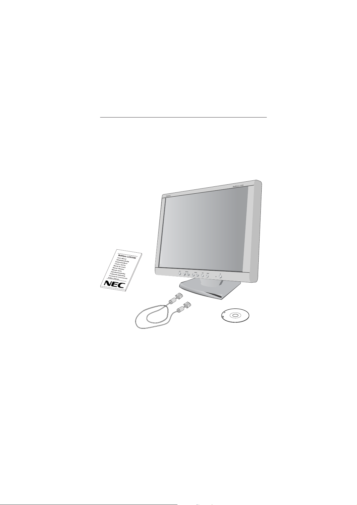
Your new NEC MultiSync LCD monitor box* should contain the following:
• MultiSync LCD1550V monitor with tilt base
• Power Cord(s)
• Video Signal Cable
• User’s Manual
• CD ROM (includes complete User’s Manual in PDF format). To see
the User’s Manual, Acrobat Reader 4.0 must be installed on your PC.
1550V
* Remember to save your original box and packing material to transport
or ship the monitor.
English-2
1-11
Page 16

Quick Start
To attach the MultiSync LCD monitor to your system, follow these
instructions:
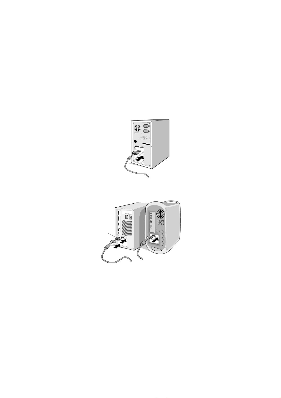
1. Turn off the power to your computer.
2. Remove connector cover and cable cover.
3. For PC: Connect the 15-pin mini D-SUB of the appropriate
signal cable to the connector for the display card in your system
(Figure A.1). Tighten all screws.
For Mac: Connect the MultiSync LCD1550V Macintosh cable
adapter to the computer (Figure B.1). Attach the 15-pin mini D-SUB
end of the appropriate signal cable to the MultiSync LCD1550V
Macintosh cable adapter (Figure B.1). Tighten all screws.
4. Connect the 15-pin mini D-SUB of the video signal cable to the
appropriate connector on the back of the monitor (Figure C.1). Place
the Video Signal Cable under Clip B.
5. Connect one end of the power cord to the MultiSync LCD Series
monitor and the other end to the power outlet. Place the video signal
cable and AC power cord under the clips (Figure C.1). Replace
connector cover and cable cover.
NOTE: Adjust the position of the cable under the clips to avoid damage
for cable or monitor.
NOTE: Please refer to Caution section of this manual for proper
selection of AC power cord.
English
6. The Vacation Switch on the right side of the monitor must be turned
on (Figure D.1). Turn on the monitor with the Power Button and the
computer.
NOTE: The Vacation Switch is a true on/off switch. If this switch is on
the OFF position, the monitor cannot be turned on using the
front button DO NOT switch on/off repeatedly.
7. No-touch auto adjust automatically adjusts the monitor to optimal
settings upon initial setup for most timings. For further adjustments,
use the following OSM controls:
• Auto Adjust Contrast
• Auto Adjust
English-3
1-12
Page 17
Refer to the Controls section of this User’s Manual for a full description
of these OSM controls.
NOTE: If you have any problems, please refer to the Troubleshooting
section of this User’s Manual.
Figure A.1
Macintosh
Cable
Adapter
(not included)
Figure B.1
English-4
1-13
Macintosh G3
and G4 do not
need a
Macintosh cable
adapter
Page 18

Figure C.1
V
0
5
5
1
Connector cover
English
Cable cover
Clip B
Power Button
Vacation Switch
Figure D.1
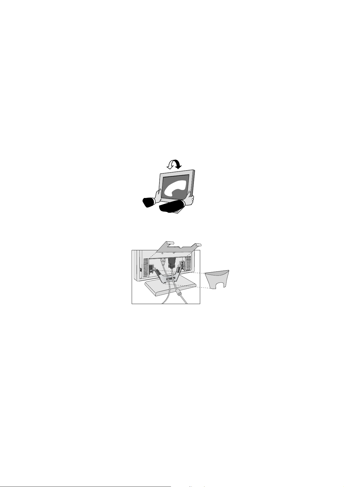
Tilt
Grasp both sides of the monitor screen with your hands and adjust the
tilt as desired (Figure TS.1).
Remove Monitor Stand for Mounting
To prepare the monitor for alternate mounting purposes:
1. Remove the connector cover and cable cover (Figure R.1).
2. Disconnect all cables.
3. Place monitor face down on a non-abrasive surface (Figure R.2).
English-5
1-14
Page 19
4. Remove the 4 screws connecting the monitor to the stand and lift off
the stand assembly (Figure R.2) the monitor is now ready for
mounting in an alternate manner.
5. Connect the AC cord and signal cable to the back of the monitor
(Figure R.3).
6. Reverse this process to reattach stand.
NOTE: Use only VESA-compatible alternative mounting method.
Figure TS.1
Figure R.1
English-6
1-15
Page 20

English
Non-abrasive
surface
Figure R.2
Figure R.3
7. This LCD monitor is designed for use with a flexible arm. Please use
the attached screws (4pcs) when mounting. To meet the safety
requirements the monitor must be mounted to an arm which
guaranties the necessary stability under consideration of the weight
of the monitor. The LCD monitor shall only be used with an approved
arm (e.g. GS mark).
English-7
1-16
Page 21
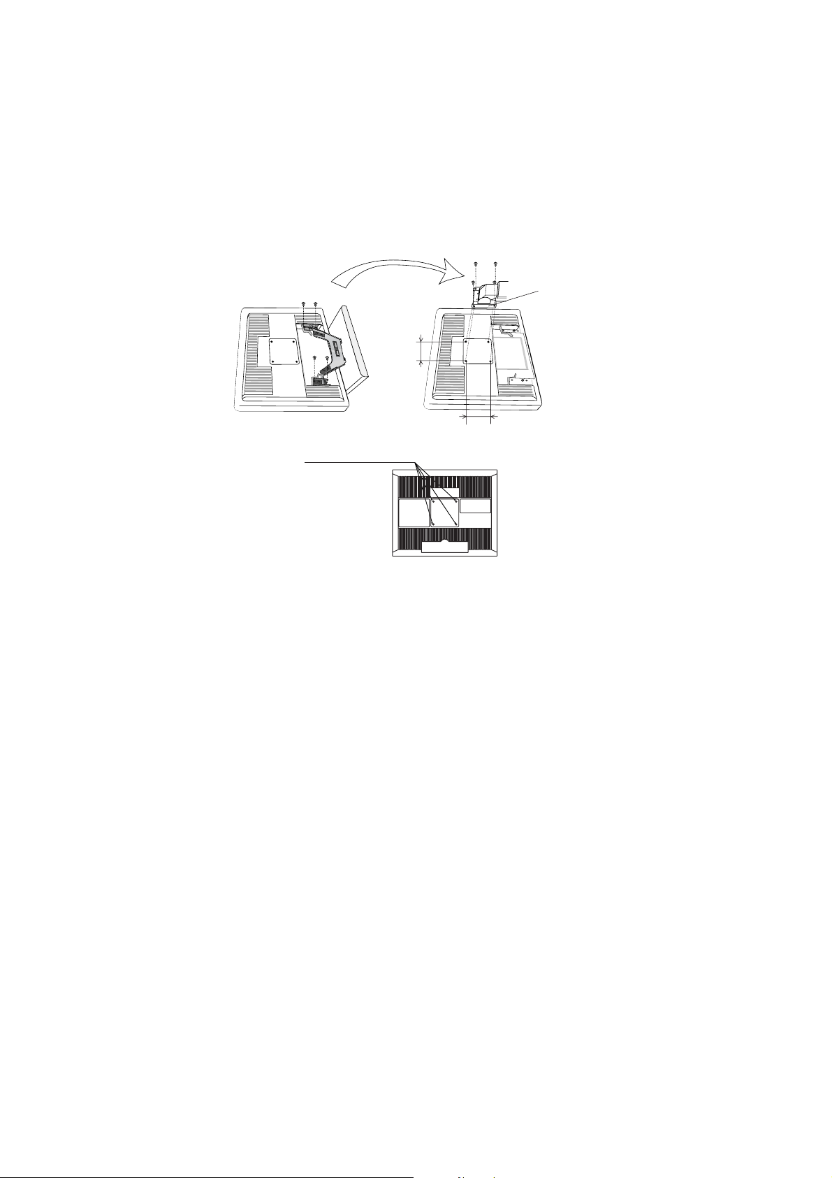
Replace screws
75 mm
75 mm
Thickness of bracket (arm)
2.0 ~ 3.2 mm
Tighten all screws
4 SCREWS (M4)
(MAX depth: 8.5 mm
If use other
screw, check
depth of hole.
)
Weight of LCD assembly: 3.2kg (MAX)
English-8
1-17
Page 22

Controls
OSM (On-Screen-Manager) Controls
The OSM controls on the front of the monitor function as follows:
To access OSM press any of the control buttons (
, , -, +, NEXT).
English
Control
EXIT
CONTROL
ADJUST -/+
NEXT
RESET
NOTE: When RESET is pressed in the main and sub-menu, a warning
window will appear allowing you to cancel the RESET function
by pressing the EXIT button.
Menu
Exits the OSM controls.
Exits to the OSM main menu.
Moves the highlighted area left/right to select control
/
menus.
Moves the highlighted area up/down to select one of the
controls.
Moves the bar left/right to increase or decrease the
adjustment.
Activates Auto Adjust function.
Enter the sub menu.
Moves the highlighted area of main menu right to select
one of the controls.
Resets the highlighted control to the factory setting.
Brightness/Contrast Controls
BRIGHTNESS
Adjusts the overall image and background screen
brightness.
CONTRAST
Adjusts the image brightness in relation to the
background.
AUTO ADJUST
Adjusts the image displayed for non-standard
video inputs.
English-9
1-18
Page 23
Auto Adjust
Automatically adjusts the Image Position, the H. Size
and Fine setting.
Position Controls
LEFT/RIGHT
Controls Horizontal Image Position within the display
area of the LCD.
DOWN/UP
Controls Vertical Image Position within the display area
of the LCD.
H. SIZE
Adjusts the horizontal size by increasing or decreasing
this setting.
FINE
Improves focus, clarity and image stability by increasing
or decreasing this setting.
Colour Control Systems
Five colour presets select the desired colour setting.
Each colour setting is adjusted at the factory.
R,G,B
Increases or decreases Red, Green or Blue colour
depending upon which is selected. The change in colour
will appear on screen and the direction (increase or
decrease) will be shown by the bars.
Tools
OSM POSITION
You can choose where you would like the OSM control
image to appear on your screen. Selecting OSM
Location allows you to manually adjust the position of
the OSM control menu left, right, down or up.
English-10
1-19
Page 24

OSM TURN OFF
The OSM control menu will stay on as long as it is use.
In the OSM Turn Off submenu, you can select how long
the monitor waits after the last touch of a button to shut
off the OSM control menu. The preset choices are 10,
20, 30, 45, 60 and 120 seconds.
OSM LOCK OUT
This control completely locks out access to all OSM
control functions. When attempting to activate OSM
controls while in the Lock Out mode, a screen will
appear indicating the OSM controls are locked out.
To activate the OSM Lock Out function, press
and hold down simultaneously. To de-activate the OSM
Lock Out, press
simultaneously.
, then and hold down
, then
RESOLUTION NOTIFIER
This optimal resolution is 1024 x 768. If ON is selected,
a message will appear on the screen after 30 seconds,
notifying you that the resolution is not at 1024 x 768.
FACTORY PRESET
Selecting Factory Preset allows you to reset all OSM
control settings back to the factory settings. The RESET
button will need to be held down for several seconds to
take effect. Individual settings can be reset by
highlighting the control to be reset and pressing the
RESET button.
English
Information
DISPLAY MODE
Indicates the current display resolution and frequency
setting of the monitor.
MONITOR INFO.
Indicates the model and serial numbers of your monitor.
English-11
1-20
Page 25

OSM Warning
OSM Warning menus disappear with Exit button.
NO SIGNAL: This function gives a warning when there
is no signal present. After power is turned on or when
there is a change of input signal or video is inactive, the
No Signal window will appear.
RESOLUTION NOTIFIER: This function gives a
warning of use with optimized resolution. After power is
turned on or when there is a change of input signal or
the video signal doesn’t have proper resolution, the
Resolution Notifier window will open. This function can
be disabled in the TOOL menu.
OUT OF RANGE: This function gives a
recommendation of the optimized resolution and refresh
rate. After the power is turned on or there is a change of
input signal or the video signal doesn’t have proper
timing, the Out Of Range menu will appear.
CHECK CABLE: This function will advise you to check
all Video Inputs on the monitor and computer to make
sure they are properly connected.
English-12
1-21
Page 26
Recommended Use
Safety Precautions and Maintenance
FOR OPTIMUM PERFORMANCE, PLEASE NOTE
THE FOLLOWING WHEN SETTING UP AND
USING THE MULTISYNC LCD COLOUR MONITOR:
• DO NOT OPEN THE MONITOR. There are no user serviceable parts
inside and opening or removing covers may expose you to dangerous
shock hazards or other risks. Refer all servicing to qualified service
personnel.
• Do not spill any liquids into the cabinet or use your monitor near water.
• Do not insert objects of any kind into the cabinet slots, as they may
touch dangerous voltage points, which can be harmful or fatal or may
cause electric shock, fire or equipment failure.
• Do not place any heavy objects on the power cord. Damage to the cord
may cause shock or fire.
• Do not place this product on a sloping or unstable cart, stand or table, as
the monitor may fall, causing serious damage to the monitor.
• Do not place any objects onto the monitor and do not use the monitor
outdoors.
• The inside of the flourescent tube located within the LCD monitor
contains mercury. Please follow the bylaws or rules of your municipality
to dispose of the tube properly.
Immediately unplug your monitor from the wall outlet and refer servicing to
qualified service personnel under the following conditions:
• When the power supply cord or plug is damaged.
• If liquid has been spilled, or objects have fallen into the monitor.
• If the monitor has been exposed to rain or water.
• If the monitor has been dropped or the cabinet damaged.
• If the monitor does not operate normally by following operating
instructions.
• Do not bend power cord.
• Do not use monitor in high temperatured, humid, dusty, or oily areas.
• Do not cover vent on monitor.
• If monitor is broken, do not come in contact with the liquid crystal.
• If glass is broken. Handle with care.
English
English-13
1-22
Page 27
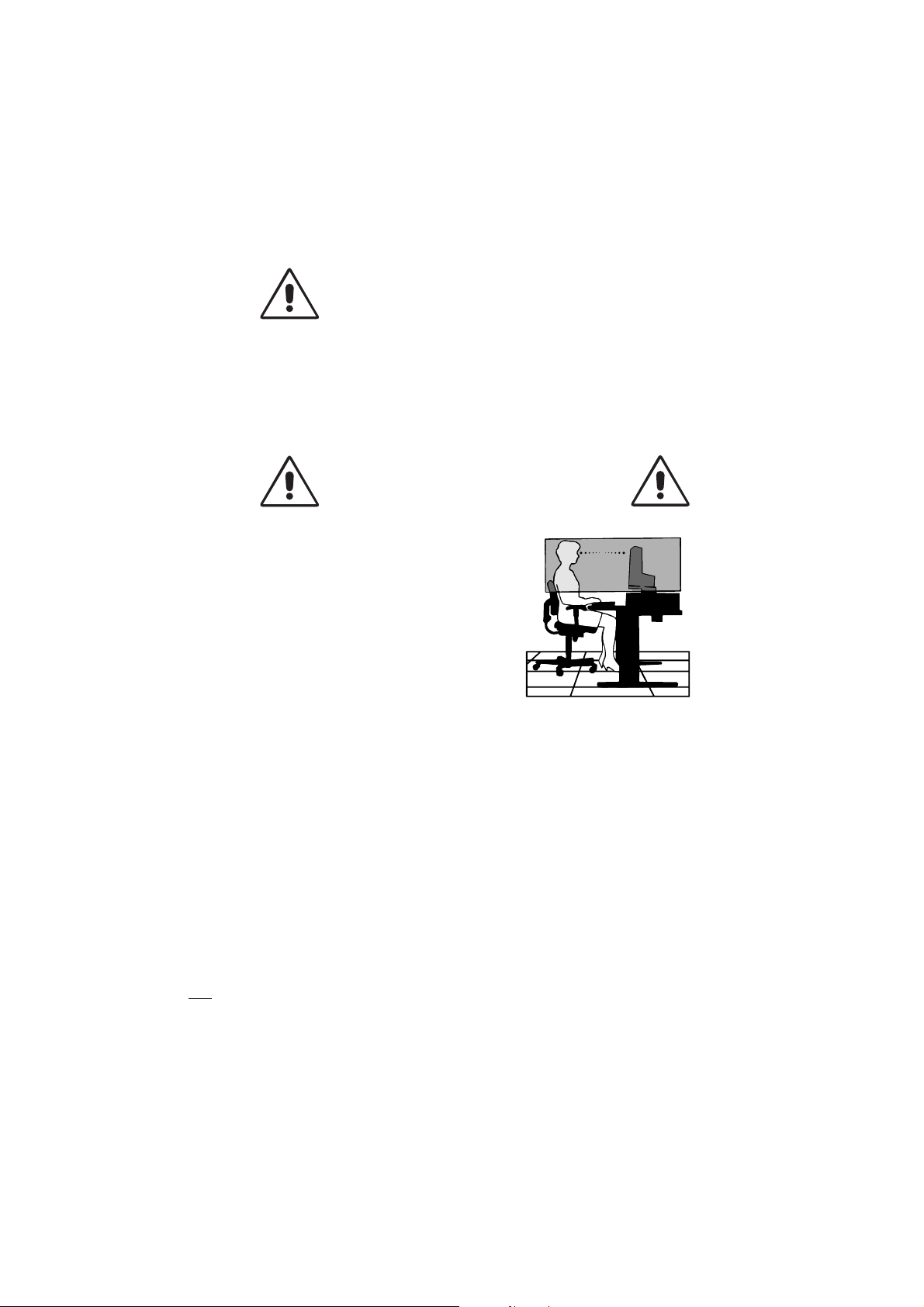
• Allow adequate ventilation around the monitor so that
heat can properly dissipate. Do not block ventilated
openings or place the monitor near a radiator or other
CAUTION
• For optimum performance, allow
20 minutes for warm-up.
• Adjust the monitor height so that the top of
the screen is at or slightly below eye level.
Your eyes should look slightly downward
when viewing the middle of the screen.
• Position your monitor no closer than 40 cm
and no further away than 70 cm from your
eyes. The optimal distance is 53 cm.
• Rest your eyes periodically by focusing on
an object at least 6 m away. Blink often.
• Position the monitor at a 90° angle to windows and other light sources to
minimize glare and reflections. Adjust the monitor tilt so that ceiling lights
do not reflect on your screen.
• If reflected light makes it hard for you to see your screen, use an
antiglare filter.
• Clean the LCD monitor surface with a lint-free, non-abrasive cloth. Avoid
using any cleaning solution or glass cleaner!
• Adjust the monitor’s brightness and contrast controls to enhance
readability.
• Use a document holder placed close to the screen.
• Position whatever you are looking at most of the time (the screen or
reference material) directly in front of you to minimize turning your head
while you are typing.
heat sources. Do not put anything on top of monitor.
• The power cable connector is the primary means of
detaching the system from the power supply. The
monitor should be installed close to a power outlet which
is easily accessible.
• Handle with care when transporting. Save packaging for
transporting.
CORRECT PLACEMENT AND ADJUSTMENT OF
THE MONITOR CAN REDUCE EYE, SHOULDER
AND NECK FATIGUE. CHECK THE FOLLOWING
WHEN YOU POSITION THE MONITOR:
English-14
1-23
Page 28

• Avoid displaying fixed patterns on the monitor for long periods of time to
avoid image persistence (after-image effects).
• Get regular eye checkups.
Ergonomics
To realize the maximum ergonomics benefits, we recommend the following:
• Use the preset Size and Position controls with standard signals.
• Use the preset Colour Setting.
• Use non-interlaced signals with a vertical refresh rate between
60-75 Hz.
• Do not use primary colour blue on a dark background, as it is difficult to
see and may produce eye fatigue to insufficient contrast.
English
English-15
1-24
Page 29

1-25
Printed in Taiwan
HD67NM55101
Page 30
Serial Number Information
r
)
Refer to the serial number information shown below.
Manufactured Year :
( Last digit )
Manufactured Month :
January to September 1 to 9
October X
November Y
December Z
Panel Code: A ~ Z (Hannstar panel)
EX.) SERIAL NUMBER LABEL
Model Name : LCD1550V-1
: LCD1550V-1-BK
SERIAL NO. :
g g g g g g g g g
Serial Number(4-digit)
(sequential numbe
at production month,
0001-9999
(White model)
(Black model)
Reference: 0~9 (LG panel)
Factory Code:
Compal Taiwan factory ...... “I”
Compal China factory ...... “T”
Control Code:
A, B
2-1
Page 31

DISASSEMBLY
g Before you disassemble the set, turn off power and pull out the power plug.
g Use the proper screwdriver. If oversize or undersize screwdriver is used, screws may be damaged.
g Assembly is the opposite process of disassembly.
SYMBOL CODE(Compal) CODE(NMV) DESCRIPTION CABINET COLOR
1 FANM5522100 79PP0619 CONNECTOR COVER NM5522 AB White
1 FANM5522200 79PP0694 CONNECTOR COVER NM5522 AB Black
2 FANM5524100 79PP0589 CABLE COVER White
2 FANM5524200 79PP0607 CABLE COVER ASSY(BK-A) Black
3 --- --- SL-CPIMS*4*12*15BF ---
1
3
2
3
3 3
3-1
Page 32

SYMBOL CODE(Compal) CODE(NMV) DESCRIPTION CABINET COLOR
4 FANM5516100 79PP0587 CABINET BACK ASSY White
4 FANM5516200 79PP0606 CABINET COVER ASSY(BK-A) Black
5 --- --- #2CPITS*3*12*3AF White
5 --- --- #2CPITS*3*12*3KF Black
4
5
5
3-2
Page 33

SYMBOL CODE(Compal) CODE(NMV) DESCRIPTION
6 --- --- CPIMS(CUP)*3*6*3AF
7 --- --- SCREW SPECIAL
8 --- --- SHIELD PCB ASSY
6
8
7
SYMBOL CODE(Compal) CODE(NMV) DESCRIPTION
5 --- --- #2CPITS*3*12*3AF
9 454A5267001 79PP0584 PCBA KEY/B VK-530 LNM555G
CN1
9
5
5
5
3-3
Page 34

SYMBOL CODE(Compal) CODE(NMV) DESCRIPTION CABINET COLOR
6 --- --- CPIMS(CUP)*3*6*3AF --10 461A7367004 79PP0860 FIRMWARE CTRL/B VL-543 LN White
10 461A7367005 79PP0868 FIRMWARE CTRL/B VL-543 LN Black
CN2
CN3
J2
6
10
J1
SYMBOL CODE(Compal) CODE DESCRIPTION CABINET COLOR
6 --- --- CPIMS(CUP)*3*6*3AF --11 --- --- SPECIAL WASHER 4*8*15BF --26 --- --- CFIMS*3*6*3KF --12 453A7367001 79PP0801 PCBA POWER/B VP-543 LNS55 --13 453A7567001 79PP0802 PCBA INVERTER/B VI-543 LN --14 DC020149900 79PP0806 H-CON SET NS555 P802-SW White
14 DC020150000 79PP0855 H-CON SET NS555 P802-SW B Black
J951
P804
6
P803
13
J901
12
J911
14
11
P802
2
3-4
Page 35

SYMBOL CODE(Compal) CODE(NMV) DESCRIPTION CABINET COLOR
5 --- --- #2CPITS*3*12*3AF --16 FANM5515100 79PP0586 CABINET FRONT ASSY White
16 FANM5515200 79PP0605 CABINET FRONT ASSY(BK-A) Black
5
16
SYMBOL CODE(Compal) CODE(NMV) DESCRIPTION
17 --- --- CPIMS*2.5**4*3AF
17
17
3-5
Page 36

SYMBOL CODE(Compal) CODE DESCRIPTION
18 AC600022900 79PP0804 LCD HSD150SX84-B 15" HANNSTAR
27 NBX40000300 79PP0808 FFC 40P G P0.5 PAD=0.5 71
27
27
18
SYMBOL CODE(Compal) CODE DESCRIPTION CABINET COLOR
19 --- --- HINGE L --20 --- --- HINGE R --21 FANM5523100 79PP0620 STAND FRONT NM5523 ABS+PC White
21 FANM5523200 79PP0695 STAND FRONT NM5523 ABS+PC Black
22 --- --- BRACKET HINGE --23 FANM5517100 79PP0618 BASE ASSY NM5517 ABS+PC M White
23 FANM5517200 79PP0693 BASE ASSY-NEC NM5517 ABS+ Black
24 --- --- SL-CPIMS*4*8*15BF --25 --- ---- SL-CPIMS*4*16*15BF ---
19
20
21
24
22
25
23
3-6
Page 37

ADJUSTMENT PROCEDURES
TABLE OF CONTENTS
Page
1. Application --------------------------------------------------------------------------------------------- 2-2
2. Adjustment conditions ------------------------------------------------------------------------------ 2-2
2.1 Time for adjustment ------------------------------------------------------------------------------- 2-2
2.2 Measuring instruments, jigs, and tools ------------------------------------------------------- 2-2
2.3 Power-supply voltage ----------------------------------------------------------------------------- 2-2
2.4 Aging -------------------------------------------------------------------------------------------------- 2-2
3. Set adjustments -------------------------------------------------------------------------------------- 2-3
3.1 Power ON -------------------------------------------------------------------------------------------- 2-3
3.2 Factory mode --------------------------------------------------------------------------------------- 2-4
3.3 Factory reset and auto contrast ---------------------------------------------------------------- 2-8
4. VG-829 Setting Method --------------------------------------------------------------------------- 2-10
2-1
Page 38

1. Application
This adjustment specification shall be applied to the adjustment of the LCD1550V (LA-15R02-1) /
LCD1550V-BK (LA-15R02-1-BK).
2. Adjustment conditions
2.1 Time for adjustment
Adjustment of a unit to be adjusted shall be carried out only at the time of the adjustment of the set as a whole.
2.2 Measuring instruments, jigs, and tools
The measuring instruments, jigs, and tools required at the time of the adjustment of the unit to be adjusted shall
be as specified below.
a. A signal generator that can generate an output of signal timing produced by the adjusted (*) VG-829 or
specified in [4. Setting method for the VG-829.] In this case, however, this signal generator shall be
capable of displaying all white and all black as a screen display pattern.
* The word “adjusted” shall mean that the amplitude of each signal R, G, B, which is output from the signal
generator, is maintained at 0.7Vp-p ± 0.05V when a load of 75Ω is connected.
b. D-SUB 15-pin signal cable
c. Video signal cable
2.3 Power-supply voltage
INPUT : 100Vac ~ 240Vac ±10%, 47~63Hz
2.4 Aging
Not required.
2-2
Page 39

3. Set adjustments
r
3.1 Power ON
1) Insert the AC power cable in a wall outlet, or press the POWER key thereafter. Confirm that the LED is lit
in amber (or that an OSM of [NO SIGNAL] is displayed).
* The product shall be regarded as an NG item unless the LED is lit in amber even when the AC power cable
is inserted in a wall outlet or the POWER key is pressed.
2) Enter an input of Signal 20. Confirm that the LED is lit in green.
* The product shall be regarded as an NG item unless the LED is lit in green at that time.
3) Press the NEXT. ADJUST or Control key, and confirm that an OSM is displayed in the LCD screen.
Information
Supplementary description
The horizontal and vertical frequency values
displayed involve the errors of ±2kHz fo
horizontal and ±2kHz for vertical.
Indicate the Input signal timing mode.
Resolution /Frequency
4
(right) : No Function
3(left) : No Function
+ (plus) : No function
- (minus) : No function
NEXT : Change tag to next right direction
RESET : No function.
EXIT : Jump to main menu
Press RESET + 3 + 4 at the same time under the condition of the above OSM to enter Factory mode.
2-3
Page 40

3.2 Factory mode
Mention the contents of the service menu letter
Warning message
How to enter Service mode
1. Open Information menu (Signal information)
2. Press “3”+”4”+”RESET”
3. Indicate warning message
4. Press Next then enter Service mode
Or Press EXIT to close OSM menu
OSM Flame is CYAN
Color of frame
Service: Cyan
How to use Service mode
Page1:
The page can check user’s HOURS RUNNING and system total’s HOURS RUNNING.
1. Press “NEXT” to move cursor on HOURS RUNNING.
2. Press “3 (LEFT)” + “RESET” at the same time can check HOURS RUNNING.
3. Press “3 (LEFT)” or “4 (RIGHT)” to move cursor on FACTORY PRESET.
4. Press “RESET” + “4 (RIGHT)” can reset all function to initial (include user’s HOURS RUNNING
and AUTO INFORMATION).
2-4
Page 41

Page2:
The page can adjust RGB offset and gain.
3
1. Press
2. Press “+” or “-“ can auto balance.
How to exit Service mode
Press exit key and then close OSM menu (Service mode)
When turn off monitor in Service mode, it should exit from Service mode.
If unplug a power cord in Service mode, it should exit from Service mode too.
: Hours Running
or 4 to move cursor on AUTO GAIN or AUTO OFFSET.
Indicate On time and Off mode (power save) time(hours, minutes).
There are two timers.
The one can be cleared and the other cannot be cleared.
Following Key operation changes the timer indication.
Select Hours Running item
RIGHT+ RESET: Indicate timer which can be cleared
LEFT+ RESET: Indicate timer which cannot be cleared
LEFT+RIGHT+RESET : Timer is cleared
The indicated number should be changed every 5minutes.
On mode time xxxH xxM
Off Mode time xxxH xxM
2-5
Page 42

Page 3
: F/W ver Indicate F/W version
: Auto ADJUST COUNT
Indicate total time that Auto Adjustment (Contrast, Auto adjust) is executed.
Value should be cleared by factory reset in Service mode menu.
: OSM Menu Change
Bar or Number of User menu should be selected in Factory mode menu.
: Factory Preset in Factory mode
When proceed key is pushed at Factory preset, Hours running and auto count is cleared.
2-6
Page 43

Page 4
In this page, it is possible to modify the display style of the OSM menu.
1) Press the 3 (left) key or the 4 (right) key to adjust the cursor to the DESTINATION, MODEL TYPE,
DESIGN, or the VCO TYPE.
2) When the + or - key is pressed, each display style is changed.
DESTINATION (The OSM menu for each destination is changed.)
0: Overseas : Shipment setting
1: (Reserve)
2: Domestic
MODEL TYPE (The MODEL name of MONITOR INFO. is changed.)
B : LCD1550V : Shipment setting
BK : LCD1550V BK : Shipment setting
M3X : RDT153X
DESIGN (The adjusting value displayed is modified into a bar or a numeral.)
BAR: The adjusting value is displayed in a bar. : Shipment setting
DBG: The adjusting value is displayed in numerals. (Debug)
VCO TYPE
CAL : Shipment setting
FIX : (For evaluation)
When finishing the factory mode:
1) When the EXIT key is pressed, the OSM menu (factory mode) is closed and the factory mode is
finished.
2) If the monitor power supply is turned off in the factory mode, the factory mode is finished.
3) Even when the power cord plug is pulled out of the wall outlet in the factory mode, the factory mode
is also finished.
2-7
Page 44

3.3 Factory reset and auto contrast
1) To display information of OSM on LCD screen.
2) Press “RIGHT” + “LEFT” + “RESET” key at same time.
3) LCD screen display warring message.
4.1) Press “exit” key will exit factory mode.
4.2) Press “NEXT” key will enter factory mode.
5) When enter factory mode and move make to FACTORY PRESET.
6) Press “PLUS” or “MINUS” key and will clear HOURS RUNNING, AUTO INFORMATION and EEPROM etc.
2-8
Page 45

7) Move make to item 2 and change input video pattern to gray scale.
8) Move make to AUTO GAIN and AUTO OFFSET.
9) Press “PLUS” or “MINUS” key can adjust RGB offset and gain.
10) Exit factory mode press “exit” key.
2-9
Page 46

4. VG-829 Setting Method
Signal VG-829
Mode
H
V
OUTPUT
PAT SEL
CHARA
PATTERN
GRAY Direction:0 L0:0 L1:17 L2:34 L3:51 L4:68 L5:85 L6:102 L7:127
DOT CLOCK [MHz] 78.75
TOTAL [DOT]
DISP [DOT]
SYNC PULSE [DOT] 96
BACK [DOT] 176
HDstrat [DOT] 0
HDwidth [DOT] 0
INTERLACE NON
TOTAL [H] 800
DISP [H] 768
SYNC PULSE [H] 3
BACK PORCH [H] 28
EQPfp [H] 0
EQPbp [H] 0
SERRATION [H] OFF
EDP [H] OFF
VDs [H] 0
VBf [H] 0
OUTPUT MODE ANALOG
NRZ/RZ NRZ
CV
HS POS
VS POS
CS NEG
HD NEG
VD NEG
RGB POS
HT POS
C NEG
VIDEO 0.70V
Set-up 0.00V
Sync 0.30V
Format
Code
Font
Cell
1312
1024
GRAY
1
82
16*16
16*16
L8:143 L9:159 LA:175 LB:191 LC:207 LD:223 LE:239
LF:255
20
2-10
Page 47

INSPECTION
1. Inspection of PLUG & PLAY communication and OSM "MONITOR INFORMATION" for model name/ serial number
1.1 A construction of System
This system should be connected as shown below.
PROGRAM
P ART No. 599910552
Signal Generator
R G B H V
AUTO ADJ I/F JIG
Part No. 599910401 (120V) (For A ver.)
Part No. 599910402 (220V) (For B ver.)
D-sub to D-Sub 15pin Signal Cable
1.2 Input Signal
Horizontal synchronization frequency : No specified.
Vertical synchronization frequency : No specified.
1.3 Programs required
PNP.EXE
PNP.INI
Program D isk
PC
Printer Cable
08109741.MDL
EDID550V.TXT
5-1
Page 48

1.4 Operational procedures
1. Start PNP.EXE from DOS mode or DOS pronto of Windows.
2. Operation key assignment
• Determine the operation mode with the F1 ~ F9 and ESC keys.
F1: (Select Model) Setting file changeover for respective models.
F4: (Read) EDID data for reading.
F5: (Write Input 1) It is not used in this model.
F8: (Write Input 2) EDID data is written in.
F9: (Write ALL) It is not used in this model.
ESC: (EXIT) End of program.
3. Press the F1 key and enter an input of setting file for the related model. Press the Enter key.
File name Model
08109741 LCD1550V
4. Writing and inspection procedures
a. Press the F8 key (Write Input 2).
b. Since the screen is changed over to the one that waits for an input of serial number, examine the serial
number of the set, enter it from the keyboard, and press the Enter key.
The message of the screen:
Model Name "LCD1550V"
Input serial number (Enter only: Use previous number)
c. EDID data writing and inspection
According to the screen commands, make connections for the connectors and change over the
signals.
The message of the screen:
Input 1 File 1 set V 42Hz N (Hit any key)
Notes: This message does not need to be followed. The D-SUB connector is connected and
arbitrary signals a received.
When the Enter key is pressed, the write and inspection of EDID data are performed.
d. Upon normal completion, a screen display is presented "OK".
e. Serial number writing for the OSM “MONITOR INFORMATION”.
* The signal cable of equipment is connected with a signal generator.
* It goes into the factory mode and returns to the user mode, without carrying out anything.
* A Display “MONITOR INFORMATION.” of the OSM, and confirm that the model name
(LCD1550V or LCD1550V BK) and serial number have been correctly written.
5-2
Page 49

1.5 EDID data file
The EDID data file text is shown below. When you write or inspect EDID for this monitor, the following table
can be used.
file name : EDID550V.TXT
0 1 2 3 4 5 6 7 8 9 A B C D E F
00 FF FF FF FF FF FF 00 38 A3 C6 65 01 01 01 01
00
25
0B
10
*1)
1E 50 54 BF EE 00 01 01 01 01 01 01 01 01 01 01
20
01 01 01 01 01 01 C3 1E 00 20 41 00 20 30 10 60
30
13 00 30 E4 10 00 00 1E 00 00 00 FD 00 37 4B 1F
40
3C 08 00 0A 20 20 20 20 20 20 00 00 00 FC 00 4E
50
45 43 20 4C 43 44 31 35 35 30 56 0A 00 00 00 FF
60
00 31
70
Note 1: address 10h Week of manufacture = Month of manufacture × 4
Note 2: address 11h Year of manufacture - 1990
01 03 08 1E 17 78 EA 7E A5 A0 58 4E 96 25
*2)
35 30 30 30 30 31 49 41 0A 20 20 20 00 49
*3)
Table 1.5 Data list
*4)
Notes 3: address 71h ~ 7Dh Serial Number (ASCII coded)
If less than 13 char, terminate with 0Ah and fill the rests with 20h.
Note 4: address 7Fh Checksum
The sum of entire 128 byte shall be equal to 00h.
5-3
Page 50

2. External inspection on the LCD module
Inspection condition is approximately 15-50cm
Viewing angle is normal to the LCD panel.
Ambient temperature is in the room temperature.
Ambient illumination is 300-500Lux.
Display characteristics
Defect type Criteria
Dark / Bright Spot
Circular Foreign Material
Visual defect
D: Diameter
N: Number
W: Horizontal width
L: Vertical high
Electrical defect
N: Number
Bright or Dark Line
Foreign Material
Polarizer / Linear Scratch
Polarizer – bubble / Peeling
Maximum Allowable Defect
Count All Types
Bright Dot Random
Bright Dot 2 Adjacent
Dark Dot Random
Dark Dot 2 Adjacent
Dark Dot 3 or More Adjacent N=0
Total Bright and Dark Dots
Minimum Distance Between Bright Dots
Minimum Distance Between Dark Dots
Minimum Distance Between Bright Dots
and Dark Dots
0.2mm≤D<0.5mm
N≤4
0.05mm≤W<0.2mm
0.3mm≤L≤3mm
N≤4
0.01mm≤W<0.2mm
1.0mm≤L≤10mm
N≤3
0.15mm≤D<0.25mm
N≤4
N≤7
N≤4
N≤2
N≤4
N≤3
N≤4
≥15mm
≥10mm
≥10mm
5-4
Page 51

Note(1): Bright dot defect description
Two adjacent
Type2
Note(2): Dark dot defect description
Two adjacent
Type2 Type3
Note(3): Dark dot defect description
Type1
Type3
Type1
Three adjacent
Type1
Type2 Type3 Type4
5-5
Page 52

Not(4): Minimum distance between dot defect
Bright dot to bright dot
<15mm
NG
Dark dot to dark dot
<10mm
NG
Bright dot to dark dot
<10mm
NG
Note(5): “Average Diameter” description
Dusts would be judged by “Average Diameter” under vertical high ≥0.1mm and horizontal width ≥0.1mm
condition.
Average Diameter D=(a+b)/2
b
a
5-6
Page 53

3. Safety Tests
Perform the following inspection tests in accordance with the standards set forth in Common Electrical
Safety Inspection Standards for Information Processing Device & Office Equipment (DSQS-009-103).
Destination : World wide
Applicable Regulations : UL1950, CSA C22.2 No 950 (C-UL), DHHS, TUV (EN60950), CE, PTB
Classification : Class I device (with safety ground), movable
Ratings : AC 100-240V, 50/60Hz,
Unless otherwise specified, rating voltage is 240V.
3.1 Ground Continuity
( It is applied to the PSU built-in set. )
Perform the test at the points indicated below and make sure that the ground continuity values are within
the prescribed range. (This test is to be performed before the electric strength test.)
1) The Ground Line of inlet shall be satisfied indicated below.
a) The color of Ground Line is spiral of green and yellow.
b) The Ground Line is connected at specified point on the chassis base with specified screw.
2) Measurement Point- Between the ground terminal of power supply cord and the chassis Screw
The standard for a decision : Less than 0.1ohm. ( Input current 25A)
3.2 Electric Strength
( It is applied to the PSU built-in set. )
Perform the tests at the points indicated below and make sure that there is no dielectric breakdown or
flashing.
Measurement Points
Make measurements between the power supply terminals (other than the ground terminal) and each
of the following points : (See note below.)
Signal cable connector shell
Chassis base
Note : The two terminals other than the ground terminal (power supply cord) must be shorted out.
The standard for a decision : Less than 10mA. ( Input voltage 1500V AC )
5-7
Page 54

3.3 Leakage Current
( It is applied to both the PSU built-in set and the set with AC adapter. )
Perform the tests at the points indicated below and make sure that the leakage current is within the
prescribed range. (This test must be performed after the electric strength test.)
Measurement Points
Make measurements between the terminals of AC inlet (other than the ground terminal) and each of
the following points :
Signal cable connector shell
Chassis base
Note : Power switch status ; "ON" and "OFF" condition.
The standard for a decision : Less than 1.5 mA. ( Input voltage 255V AC (60Hz))
Measurement condition : The leakage ammeter builds in the resistor of 1500 ohm, and uses a thing
with the bypass condenser of 0.15uF.
3.4 Insulation Resistance
( It is applied to the PSU built-in set. )
Perform the tests at the points indicated below and make sure that the insulation resistance is within the
prescribed range. (This test must be performed after the electric strength test.)
Measurement Points
Make measurements between the power supply terminals (other than the ground terminal) and each
of the following points : (See note below.)
Signal cable connector shell
Chassis base
Note : The two terminals other than the ground terminal (Power supply cord) must be shorted out.
The standard for a decision : More than 30Mohm. (Input voltage 500V DC)
5-8
Page 55

TROUBLE SHOOTING
TABLE OF CONTENTS
1. No display of screen (Screen is black, color of LED is amber) ------------------------- 6-2
2. Nothing displays on screen (Screen is black, color of LED is green) ----------------- 6-3
3. Checking the back light unit --------------------------------------------------------------------- 6-6
4. Abnormal screen ---------------------------------------------------------------------------------- 6-7
5. No OSM display ----------------------------------------------------------------------------------- 6-9
6. Abnormal Auto adjustment ---------------------------------------------------------------------- 6-10
7. Abnormal plug and play operation ------------------------------------------------------------ 6-11
7.1 Abnormal DDC2 ---------------------------------------------------------------------------------- 6-11
8. Checking the interface circuit of sync signal ------------------------------------------------ 6-12
8.1 Checking the control circuit of horizontal sync pulse ------------------------------------ 6-12
Page
8.2 Checking the control circuit of vertical sync pulse --------------------------------------- 6-13
9. Checking the resolution change IC movement --------------------------------------------- 6-14
10. No power on -------------------------------------------------------------------------------------- 6-15
11. Checking the operation of CPU --------------------------------------------------------------- 6-16
6-1
Page 56

1. No display of screen (Screen is black, color of LED is amber)
Y
Does OSM display when you
push “NEXT, Adjust or Control”
button.
When a signal isn't being inputted, it is indicated with "NO SIGNAL".
It is indicated with "OUT OF RANGE" at the time of the frequency that it
can't be distinguished.
NO
Proceed section 4 “No OSM
display”.
ES
Check if the sync signal from Computer is output
and if the video cable is connected normally.
NG
OK
Proceed section 9 “Checking the resolution
change IC movement”.
Input the sync signal of computer, or
change the cable.
6-2
Page 57

2. Nothing displays on screen (Screen is black, color of LED is green)
g
)
Does computer output RGB
video si
Check OSM menu is displayed on screen
when you push the “NEXT, Adjust or
Control” key.
Is backlight lit?
NG
OK
nals?
NG
OK
NG
Refer to section 3
“Checking the backlight unit.
Check the video cable for failure.
Check the host for output signal with all black only.
1) Change pattern of video signal output on the host.
2) Reconnect the video cable.
3
Change the video cable.
Check if the LCD video signal cable is connected
between the MAIN board and LCD module.
OK
Proceed section 4
“Abnormal screen“.
OK
Next page
NG
Failure point
The cable is disconnected.
6-3
Page 58

Continue
Is 5V-source voltage provided to pins 1 and 2 of J2 in
MAIN board.
OK
NG
Is 5V-source voltage provided to pins 1
and 2 of P803 in SW REG board.
OK
Failure point
J2 cable pulled out or disconnected
Is a dot clock being outputted under the condition that a
LCD module is connected to CN2 and CN3 pin 26?
NG
OK
Check the STH pulse of negative polarity is
output on CN2 pin 29 at TTL level.
OK
NG
Check the STV1 and STV2 of negative
polarity are ouput on CN2 pin 35, 36.
NG
OK
NG
Failure point
Error in SW REG board.
Failure point
1) U3 failure.
2) Printed wire broke between
U3 and CN2, CN3 pin26.
3)L10, R63, L11 or R64 failure
Failure point
1) U3 failure.
2) Printed wire broke between
U3 and CN2 pin 29.
3) R68 or L14 failure
Failure point
1) U3 failure.
2) Printed wire broke between
U3 and CN2 pin 35, 36.
3)R72, R73, L18 or R25 failure
next page
6-4
Page 59

Continue
Check the LOAD, POL, REV, CPV, OE of positive
polarity are ouput on CN2 pin 30, 31, 32, 37, 38.
NG
OK
Check the data signal output on CN3 and CN2 R, G,
B data pin.
NG
OK
Failure point
1) U3 failure.
2) Printed wire broke between U3 and
CN3 pin 30, 31, 32, 37, 38.
3)R69, 70, 71, 74, 75, L15,16, 17, 20
or L21 failure
Failure point
1) U3 failure.
2) Printed wire broke between
U3, CN2 and CN3 data line.
Failure point
The cable broke between CN2, CN3 and LCD module.
6-5
Page 60

3. Checking the back light unit
Is 12V-source voltage provided
to pins 1 and 2 of P804 in SW
REG board?
OK
Is 12V-source voltage provided
to pins 1 and 2 of J901 in
inverter board?
OK
Check the ON/FF signal of equal “H” at J901 pin3?
OK
Check F901 open
NG
NG
NG
Error in SW REG board.
Failure point
Inverter cable disconnection.
1) u-p failure
2) printed wire broke between u-p trace to P804 pin3
OK
NG
1) Inverter cable disconnection.
2) C915, C955 open
Failure point
F901 failure. Replace the
inverter board
NG
Failure point
Failure point
6-6
Page 61

4. Abnormal screen
p
Check the R, G, B video signal from computer
in
ut on D-Sub R,G,B connector.
OK
Check the R,B,G input signals on U3 pin 17, 24,
30,respectively that their level is 0.7Vp-p
maximum.
OK
OK
Is the pulse of the TTL level being out put to
CN2 and CN3 from the data line of U3?
OK
Check the negative STH sync pulse output to
CN2 pin 29 from U13 pin 92 at TTL level.
OK
Check the negative STV1 and STV2 sync pulse
output to CN2 pin35 from U3 pin 83, 84 at TTL
level.
OK
NG
NG
NG
NG
NG
Check the positive sync pulse output LOAD,
POL, REV, CPV, OE to CN2 pin 30, 31, 32, 37,
38 from U3 pin 91, 90, 85, 82 at TTL level.
OK
NG
Next Page
Failure point
1) No R, G and B video signal output from host
computer. Check computer.
2) Video signal cable disconnection.
Failure point
In the case of the Red signal. (A Green and
Blue signal is the same path, too.)
Printed wire broke between D-Sub(R,G,B) and
U3 pin 17,24,30.
Failure point
Printed wire broke between U3 data line and
CN2,CN3.
Failure point
Printed wire broke between U3 pin 92 and CN2
pin 29.
Failure point
Printed wire broke between U2 pin 35, 36 and
CN2 pin 25, 36.
Failure point
Printed wire broke between U3 pin 91, 90, 85,
82, 81 and CN2 pin 30, 31, 32, 37, 38.
6-7
Page 62

Continue
Check the CPH clock output to CN2 and CN3
pin 26 from U3 pin 123 at TTL level.
NG
OK
Proceed section 9 “Checking the resolution
change IC movement”.
Failure point
Printed wire broke between U3 pin 123
and CN2, CN3 pin 26.
6-8
Page 63

5. No OSM display
p
Check the output of pulse from U3 pin105 ~118 and pin 124 ~ 140
when
ress NEXT, ADJUST or CONTROL key.
NG
OK
Proceed section 9 “Checking the resolution
change IC movement”
Printed wire broke between U3 pin105 ~ 118, 124 ~
140 and CN2, CN3.
6-9
Page 64

6. Abnormal Auto adjustment
Check the input of pulse from U3 pin 49 ~ 61, 67 ~75.
OK
Proceed section 9 “Checking the resolution change IC movement”.
NG
Check the output of pulse from U6 pin 3, 4, U7 pin 3, 4, 7, 8, 13, 14, 17, 18.
OK
NG
1) Printed wire broke between U6 pin 2, 5 and U8 pin 2, 30.
2) Printed wire broke between U7 pin 2, 5, 6, 9, 12, 15, 16, 19 and
U8 pin 13~15, 17 ~ 21.
Check the output of
pulse from U3 pin
49 ~ 61, 67 ~75
Failure point
OK
Failure point
(1) Printed wire broke between
U6 pin 3,4 and U3 pin 49,
50.
(2) Printed wire broke
between U7 pin 3, 4, 7, 8,
13, 14, 17, 18 and U3 pin
51 ~ 58, 67 ~ 75.
6-10
Page 65

7. Abnormal plug and play operation
7.1 Abnormal DDC2
Confirm the output of serial data on U9 pin 6 synchronize
SCLK at TTL level.
OK
1) The host machine isn't communicating in DDC2 mode.
2) The video cable may have failed or may not to have
connections for DDC.
3) Between U19 pin 6 and CN1 pin 15 may have failed.
4) Cable failure.
NG
Failure point
U9 failure.
Failure point
6-11
Page 66

8. Checking the interface circuit of sync signal
8.1 Checking the control circuit of horizontal sync pulse
Check the horizontal sync signal on U1 pin 1 at TTL
level.
OK
Check the hovizuntal sync signal on U3 pin 206 a
TTL level.
OK
Procees section 9 “Checking the resolution change
IC movement”
NG
NG
Failure point
1) No separate sync or composite sync
output by host. (Confirm the host,
output the sync signal.)
2) Video cable may have failed.
3) Printed wire broke between CN1 pin
13 and U13 pin 30.
4) R10, R38, L14, R74 open.
5) U12 failure.
Failure point
U3 failure
6-12
Page 67

8.2 Checking the control circuit of vertical sync pulse
Check the vertical sync signal on U1 pin 11
at TTL level.
NG
OK
1) No separate sync output signal from the host.(Check the
2) Video cable may have failed.
3) Printed wire broke between CN1 pin 14 and U1 pin 11.
4) R10 open.
5) U1 failure
Proceed section 9 “Checking the resolution
change IC movement”.
Failure point
host.)
6-13
Page 68

9. Checking the resolution change IC movement
Is there +3.3V supply on U3 pins 65, 76, 86, 121, 143, 157, 167, 198, 193, 183, 179, 175, 188.
Is there +2.5V supply on U3 pins 5, 7, 10, 11, 12, 15, 18, 21, 22, 25, 28, 31, 35, 36, 42, 63, 76,
88, 119, 141, 159, 162, 163, 166, 169, 170, 189, 190, 196.
OK
Is 14.318MHz clock input to U3 pin 3, 4 at
TTL level.?
OK OK
Proceed section 11 "Checking the
operation of CPU"
NG
NG
Is 14.318MHz clock output from Y1 at TTL
level.?
Failure point
Y1 failure
Proceed section 11 "Checking the
operation of CPU"
6-14
Page 69

10. No power on
Check the +12V power provided from SW REG
board.
Check the +5V power from SW REG board.
OK
Is LED turned on in amber momentarily when
power button is pushed.
OK
Proceed section 11 "Checking the operation of
CPU".
OK
NG
NG
NG
Failure point
SW REG board failure.
Failure point
SW REG board failure.
Failure point
SW REG board failure.
6-15
Page 70

11. Checking the operation of CPU
Is there +5.0V supply on U8 pin 32.
OK
OK
NG
Printed wire broke between output J2 pin1, 2 and U8
power supply pin 32.
Is 14.318MHz clock input to U3 pin 3, 4 at TTL level?
NG
Failure point
Y1 failure.
Failure point
U3 failure.
Failure point
6-16
Page 71

CIRCUIT DESCRIPTION
TABLE OF CONTENTS
Page
1. Power Circuit ------------------------------------------------------------------------------------- 7-2
1.1 Power input block ------------------------------------------------------------------------------ 7-2
1.2 Power control block --------------------------------------------------------------------------- 7-2
2. Microcomputer Control Circuit ---------------------------------------------------------------- 7-2
2.1 Clock circuit ------------------------------------------------------------------------------------- 7-2
2.2 Microcomputer port circuit ------------------------------------------------------------------- 7-2
2.3 PIO (General-purpose port) ----------------------------------------------------------------- 7-2
3. Input Image Enlargement Display Circuit -------------------------------------------------- 7-3
3.1 Jag-D ---------------------------------------------------------------------------------------------- 7-3
4. EEPROM Control Circuit ---------------------------------------------------------------------- 7-3
4.1 Data memory ------------------------------------------------------------------------------------ 7-3
5. Auto-adjuster circuit control ------------------------------------------------------------------- 7-3
5.1 Video level adjusting function --------------------------------------------------------------- 7-3
7-1
Page 72

1. Power Circuit
1.1 Power input block (Circuit diagram: SW REG board)
A power supply for internal 12V and 5V are gained from the power connector through the voltage
supervisory circuit.
1.2 Power control block
1.2.1 Basic power control
SW REG board is used to generate the system power. It have built in PWM controllers to provide two
voltage output, one is provided for microprocessor or other TTL level IC (+5V) etc., the other one is provided
for the power of inverter (+12V). These two supply power used the same oscillation frequency, the same
start-up circuit, and the same protection circuit, so they can avoid the interference each other.
1.2.2 3.3V power control (Circuit diagram: MAIN Board P.4/5)
The U11,U10 are DC converter for the 3.3V power system. It output fixed 3.3V. The U16 is a DC converter
for 2.5V power system. It out fixed 2.5V.
3.3V power are fed to S9050,and panel. 2.5V power is only fed to S9050.
1.2.3 LCD panel 3.3V power control (Circuit diagram: MAIN Board P.5/5)
Panel power control used Q6 and U15 from S9050(pin_94) PENVDD.
When the PENVDD stays at the high level, the Panel voltage is 3.3V .
When the PENVDD stays at the low level, the Panel voltage is 0V .
(Circuit diagram:
MAIN Board)
2. Microcomputer Control Circuit
2.1 Clock circuit (Circuit diagram: MAIN Board P.3/5)
The Y1 is a crystal the microcomputer. It generates an output of 14.318MHz.
2.2 Microcomputer port circuit (Circuit diagram: MAIN Board P.3/5 and P.1/5)
S9050 has an embedded Microcontroller link to U8 Flash Rom.
2
2.2.1 I
2.2.2 S9050 and Flash ROM communication buses
C buses
U3 (PIN40) (GPIO2) SDDAT Serial data
U3 (PIN39) (GPIO1) SDCLK Serial clock
2
This is an I
U3 (PIN75) MCAD0
U3 (PIN74) MCAD1
U3 (PIN73) MCAD2
U3 (PIN72) MCAD3
U3 (PIN71) MCAD4
U3 (PIN70) MCAD5
U3 (PIN69) MCAD6
U3 (PIN68) MCAD7
U3 (PIN67) MCA8
U3 (PIN57) MCA9
U3 (PIN56) MCA10
C serial communication bus and is used for R or W data communication of U2 and U9.
U3 (PIN55) MCA11
U3 (PIN54) MCA12
U3 (PIN53) MCA13
U3 (PIN52) MCA14
U3 (PIN51) MCA15
U3 (PIN50) MCAD16
U3 (PIN49) MCAD17
U3 (PIN61) CS0#
U3 (PIN60) MCWR#
U3 (PIN59) MCRD#
7-2
Page 73

2.3 PIO (General-purpose port) (Circuit diagram: MAIN Board P.3/5)
2.3.1 Key scan status
U3 GPIO20 (pin 203) Key2-1 and GPIO 17 (pin 80) Key1-2 output pulses continuously. If Keys are pressed,
microcomputer will detect U3 signal to judge which key is pressed.
2.3.2 D-sub cable status signal
U3 GPIO5 (PIN96) CABLE-DETECT
This is an IN/OUT supervisory signal for the D-sub cable.
It is set at the low level when the cable is connected.
2.3.3 LED control
U3 GPIO3 (PIN41) LEDY
U3 GPIO19 (PIN78) LEDG
These signals are used for the LED lighting control.
When GPIO3 is high the LEDY lit and GPIO19 is low the LEDG lit.
3. Input Image Enlargement Display Circuit
3.1 S9050 (Circuit diagram: MAIN Board P.1/5)
The S9050 (U3) is controlled through the internal microcomputer.
The S9050 is provided with the analog interface D-SUB (CN1) and the digital interface.
4. EEPROM Control Circuit
4.1 Data memory (Circuit diagram: MAIN Board P.3/5)
The display control data are held by the EEPROM (U9). These display control data are accessed through
the IIC bus of the microcomputer.
5. Auto-adjuster circuit control
5.1 Video level adjusting function
Functions of VIDEO RAM are also used for the automatic contrast adjustment (video level adjustment).
For the microcomputer, a maximum value of the entered one screen or the level data in the specified area
can be used.
This readout value is used for the black level setting and white level setting (contrast setting) for the VIDEO
amplifier.
7-3
Page 74

REPLACEMENT PARTS LIST
)
V
The components specified for Model LCD1550V-1(B
SYMBOL Part No for Compal Part No forNM
*** ICS ***
U1 SA074140400 79PP0843 S IC SN74LVC14 SOP-14 INV
U10 SA011170300 79PP0842 S IC APL1117-33VC-TR SOTU11 SA010840200 79PP0841 S IC AIC1084-33CE TO252-3
U12 SA744066000 79PP0484 SM IC 74HC4066D SOP-14 AN
U13 SA011170200 79PP0626 IC APL1117-25 SOT-223 2.5
U14 SA011170200 79PP0626 IC APL1117-25 SOT-223 2.5
U15 SB923050000 79PP0846 S TR SI2305DS-T1 1P SOT-2
U2 SA024210300 79PP0627 IC EE 128X8 SOP-8 24LC21A
U3 SA090500000 79PP0844 S IC S9050-100 QFP-208
U4 SA007810010 79PP0840 FS781 BZB SOP-8 SPREAD CL
U5 SA008100300 79PP0625 IC LM810M3X-4.38 SOT-23
U6 SA7437382T2 79PP0845 S IC 74HCT373 (SSOP-20)
U7 SA7437382T2 79PP0845 S IC 74HCT373 (SSOP-20)
U8 SA002610000 79PP0839 S IC EPROM PLCC-32 MX26C1
U800 AB008170000 79PP5290 IC LTV-817M-B DIP-4 PHOTO
U801 AB038420404 79PP5021 IC KA3842A DIP-8 PWM
U802 AB0043101T3 79PP5289 IC KA431Z TO-92 REGULATOR
U9 SA024160008 79PP0359 IC EE 16K SO-8 C
U901 SA097410000 79PP0632 IC BA9741F SOP-16 PWM
DESCRIPTION
*** TRANSISTORS ***
Q1 SBX012400T0 79PP0058 TR DTC124EK (SOT-23)
Q2 SBX012400T0 79PP0058 TR DTC124EK (SOT-23)
Q3 SB7700200T5 79PP0189 TR 2N7002
Q4 SB1103600T3 79PP0055 TR 2SA1036K (SOT-23)
Q5 SB7700200T5 79PP0189 TR 2N7002
Q6 SBX012400T0 79PP0058 TR DTC124EK (SOT-23)
Q801 BB527610001 79PP5310 TRANSISTOR 2SK2761-01MR 1
Q802 BB3014500T7 79PP0735 TR HTL145 NPN TO-92
Q803 BB30945P1T5 79PP5028 TRANSISTOR 2SC945-P
Q804 BC9T169D0T7 79PP5323 SCR BT169D TO-92
Q901 SB3241100T8 79PP0057 TR 2SC2411K (SOT-23)
Q902 SB8A12400T1 79PP0635 TR DTA124EK (SM)
Q911 SB3241100T8 79PP0057 TR 2SC2411K (SOT-23)
Q912 SB8A12400T1 79PP0635 TR DTA124EK (SM)
Q913 SB3467200T3 79PP0634 TR 2SC4672 (SOT-89)
Q914 SB3467200T3 79PP0634 TR 2SC4672 (SOT-89)
Q915 SB7700200T5 79PP0189 TR 2N7002
Q916 SB934570000 79PP0636 TR SI3457DV-T1 1P TSOP-6
Q951 SB3241100T8 79PP0057 TR 2SC2411K (SOT-23)
Q952 SB8A12400T1 79PP0635 TR DTA124EK (SM)
8-1
Page 75

SYMBOL Part No for Compal Part No forNM
V
DESCRIPTION
Q953 SB3467200T3 79PP0634 TR 2SC4672 (SOT-89)
Q954 SB3467200T3 79PP0634 TR 2SC4672 (SOT-89)
Q955 SB7700200T5 79PP0189 TR 2N7002
Q956 SB934570000 79PP0636 TR SI3457DV-T1 1P TSOP-6
*** DIODES ***
BD801 BC3BP08M100 79PP0814 DIO (BR) 2KBP08M PANJIT
D1 SC10QS041T4 79PP0061 DIODE EC10QS04
D2 SC10QS041T4 79PP0061 DIODE EC10QS04
D3 SC4LZ56B0T5 79PP0380 ZENER DIODE RLZ5.6B(LL-34
D4 SC4LZ56B0T5 79PP0380 ZENER DIODE RLZ5.6B(LL-34
D5 SC4LZ56B0T5 79PP0380 ZENER DIODE RLZ5.6B(LL-34
D6 SC4LZ56B0T5 79PP0380 ZENER DIODE RLZ5.6B(LL-34
D801 BC1PS1010T0 79PP0832 DIO PS1010R DO-41 PANJIT
D802 BC1PS1040T0 79PP0833 DIO PS104R DO-41 PANJIT
D803 BC11N4148T8 79PP0258 DIODE 1N4148
D804 BC11N4148T8 79PP0258 DIODE 1N4148
D805 BC11N4148T8 79PP0258 DIODE 1N4148
D806 BC11N4148T8 79PP0258 DIODE 1N4148
D841 BC1ER100200 79PP0736 DIODE ER1002F T0-220F
D842 BC1SB5600N0 79PP0813 DIO SB560-F17 DO-201AD P2
D901 SC11N4148T8 79PP0062 DIODE 1N4148 (SM)
D910 SC11N4148T8 79PP0062 DIODE 1N4148 (SM)
D911 SC10QS042T4 79PP0825 S DIO EC10QS04
D912 SC6BAV99100 79PP0826 S DIO ROW BAV99(JE) 2P SO
D950 SC11N4148T8 79PP0062 DIODE 1N4148 (SM)
D951 SC10QS042T4 79PP0825 S DIO EC10QS04
D952 SC6BAV99100 79PP0826 S DIO ROW BAV99(JE) 2P SO
LED401 BC5G2093000 79PP0331 LED LYG2093 YEL/GRN 3D
ZD1 SC1LC208000 79PP0376 DIODE DALC208SC6 SOT23-6
ZD801 BC4HZ2020T7 79PP0834 ZEN DIO HZ20-2
*** TRANSFORMERS ***
T801 DG100015100 79PP0771 X'FORMER NM555 POWER EFD2
T911 SP051006200 79PP0831 S X'FORM NS555 EFD20 POWE
T951 SP051006200 79PP0831 S X'FORM NS555 EFD20 POWE
*** VARIABLE RESISTORS ***
VR801 CF210010201 79PP5233 VR 1/10W 1KB VZ068TL1-B1K
*** RELAYS & SWITCHES ***
SW1 DE611001500 79PP0615 TACT SW NM555 SKHHBW2720
SW2 DE611001500 79PP0615 TACT SW NM555 SKHHBW2720
SW3 DE611001500 79PP0615 TACT SW NM555 SKHHBW2720
SW4 DE611001500 79PP0615 TACT SW NM555 SKHHBW2720
SW5 DE611001500 79PP0615 TACT SW NM555 SKHHBW2720
SW6 DE611001500 79PP0615 TACT SW NM555 SKHHBW2720
SW7 DE611001500 79PP0615 TACT SW NM555 SKHHBW2720
8-2
Page 76

SYMBOL Part No for Compal Part No forNM
V
DESCRIPTION
SW8 DE611001500 79PP0615 TACT SW NM555 SKHHBW2720
*** PWB ASSYS ***
CTRLBD 461A7367004 79PP0860 FIRMWARE CTRL/B VL-543 LN
INVBD 453A7567001 79PP0802 PCBA INVERTER/B VI-543 LN
KEYBD 454A5267001 79PP0584 PCBA KEY/B VK-530 LNM555G
POWBD 453A7367001 79PP0801 PCBA POWER/B VP-543 LNS55
*** COILS & FILTERS ***
CORE DC150010200 79PP0807 CORE KC K5B FS 25.5X4.5X
L1 SM010014200 79PP0491 SSUPPRE KC FBM-L11-160808
L12 SM060000500 79PP0668 SUPPRE NWE STC222B
L13 SM010006300 79PP0447 CHIP MURATA BLM21P300S
L2 SM010014200 79PP0491 SSUPPRE KC FBM-L11-160808
L22 SM010007200 79PP0136 COIL BLM21P221SG
L3 SM010014200 79PP0491 SSUPPRE KC FBM-L11-160808
L4 SM010007200 79PP0136 COIL BLM21P221SG
L5 SM010007200 79PP0136 COIL BLM21P221SG
L6 SM010007200 79PP0136 COIL BLM21P221SG
L7 SM010007200 79PP0136 COIL BLM21P221SG
L8 SM010007200 79PP0136 COIL BLM21P221SG
L801 CL900006805 79PP0769 LINE FILT BJ350 5MH 1.2A
L802 CL900006805 79PP0769 LINE FILT BJ350 5MH 1.2A
L803 DC1510009T0 79PP5278 BEAD NWE W5 3.5X6X1.0+T
L841 CL300003600 79PP0768 CHOK COIL NM555 2.9UH +-3
L842 CL300003600 79PP0768 CHOK COIL NM555 2.9UH +-3
L9 SM010006300 79PP0447 CHIP MURATA BLM21P300S
L911 CL310011600 79PP0613 CHOK COIL NM555 245UH K
L951 CL310011600 79PP0613 CHOK COIL NM555 245UH K
*** ELECTRICAL PARTS & MISCELLANEOUS PARTS ***
CABLAS DC190020600 79PP0614 CB ASY NM555 20276/2CORE
CABLCT DC020145400 79PP0699 H-CON SET NM555 CTRL-KEY
CABLSW DC020149900 79PP0806 H-CON SET NS555 P802-SW
CN2 SP02E002100 79PP0670 W-CONN E&T 98210-4011 40P
CN3 SP02E002100 79PP0670 W-CONN E&T 98210-4011 40P
F801 DX202P02135 79PP0772 FUSE 2AH 250V S UL/SENKO/
F901 SP0402P3000 79PP0830 S FUSE 2.3A 50V UL/CSA FA
FFC NBX40000300 79PP0808 FFC 40P G P0.5 PAD=0.5 71
P801 DC040011700 79PP0791 SOCKET POWER SA-4S-066
PWRC GA020000160 79PP0674 PWR CORD SP022X2.0MXIS14
VA801 DC350001700 79PP0770 ABSORBER PANASONIC ERVZ07
Y1 BD114P3M010 79PP0610 CRYSTAL 14.31818MHZ HC-49
LCD AC600022900 79PP0804 LCD HSD150SX84-B 15" HANNSTAR
*** APPEARANCE PARTS ***
BASE FANM5517100 79PP0618 BASE ASSY NM5517 ABS+PC M
CABB FANM5516100 79PP0587 CABINET BACK ASSY
8-3
Page 77

SYMBOL Part No for Compal Part No forNM
V
DESCRIPTION
CABCV FANM5524100 79PP0589 CABLE COVER
CABF FANM5515100 79PP0586 CABINET FRONT ASSY
CONCV FANM5522100 79PP0619 CONNECTOR COVER NM5522 AB
STAF FANM5523100 79PP0620 STAND FRONT NM5523 ABS+PC
CHASS EENS5518100 79PP0817 CHASSIS BASE ASSY NM5518
*** PRINTED & PACKING MATERIALS ***
CART HB4NM555810 79PP0863 CARTON C-NM555-J67 FOR B/
CAUTI HF6NM555500 79PP0678 CAUTION SHEET F-NM555-J67
CDD LC55NM55A10 79PP0865 CD DISK NM555-J67 FOR B/B
MANU HD67NM55110 79PP0862 USER'S MANUAL U-NM555-J67
PEBAG HK3NJ350000 79PP0295 PE BAG
RAT EJ4NS550200 79PP0861 RATING NP N-NS555-J67 TCO
SALES HF6NJ350120 79PP0864 SALES OFFICE LIST F-NJ350
SETUP HF6NM555100 79PP0677 SET UP SHEET F-NM555-J67
SPB FJNM5515400 79PP0716 SPACER B
SPT FJNM5515300 79PP0715 SPACER T
*** RESISTORS ***
L10 SD013220AT4 79PP0101 R,CHIP 22H 1/16W +-5%
L11 SD013220AT4 79PP0101 R,CHIP 22H 1/16W +-5%
L14 SD0130000T4 79PP0092 R,CHIP 0H 1/16W +5%
L15 SD0130000T4 79PP0092 R,CHIP 0H 1/16W +5%
L16 SD0130000T4 79PP0092 R,CHIP 0H 1/16W +5%
L17 SD0130000T4 79PP0092 R,CHIP 0H 1/16W +5%
L18 SD0130000T4 79PP0092 R,CHIP 0H 1/16W +5%
L19 SD0130000T4 79PP0092 R,CHIP 0H 1/16W +5%
L20 SD0130000T4 79PP0092 R,CHIP 0H 1/16W +5%
L21 SD0130000T4 79PP0092 R,CHIP 0H 1/16W +5%
R1 SD014100009 79PP0850 S RES 1/16W 100 +-1% 0603
R10 SD014100009 79PP0850 S RES 1/16W 100 +-1% 0603
R11 SD0132201T1 79PP0100 R,CHIP 2.2K 1/16W +-5%
R12 SD0132201T1 79PP0100 R,CHIP 2.2K 1/16W +-5%
R13 SD013270202 79PP0394 CHIP RES 1/16W 27K +-5%
R14 SD0134702T5 79PP0102 R,CHIP 47K 1/16W +-5%
R15 SD0131002T3 79PP0096 R,CHIP 10K 1/16W +-5%
R16 SD014100009 79PP0850 S RES 1/16W 100 +-1% 0603
R17 SD014100009 79PP0850 S RES 1/16W 100 +-1% 0603
R18 SD013220AT4 79PP0101 R,CHIP 22H 1/16W +-5%
R19 SD013220AT4 79PP0101 R,CHIP 22H 1/16W +-5%
R2 SD014750A03 79PP0415 CHIP RES 1/16W 75 +-1%
R20 SD0131002T3 79PP0096 R,CHIP 10K 1/16W +-5%
R21 SD0131004T8 79PP0190 CHIP RES 1/16W 1M +-5% 06
R22 SD0131001T6 79PP0095 R,CHIP 1K 1/16W +-5%
R23 SD0131001T6 79PP0095 R,CHIP 1K 1/16W +-5%
R24 SD013470A07 79PP0849 S RES 1/16W 47 +-5% 0603
R25 SD0130000T4 79PP0092 R,CHIP 0H 1/16W +5%
R26 SD013100AT9 79PP0098 R,CHIP 10H 1/16W +-5%
8-4
Page 78

SYMBOL Part No for Compal Part No forNM
V
DESCRIPTION
R27 SD013100AT9 79PP0098 R,CHIP 10H 1/16W +-5%
R28 SD0131002T3 79PP0096 R,CHIP 10K 1/16W +-5%
R29 SD0131002T3 79PP0096 R,CHIP 10K 1/16W +-5%
R3 SD014100009 79PP0850 S RES 1/16W 100 +-1% 0603
R30 SD013220AT4 79PP0101 R,CHIP 22H 1/16W +-5%
R31 SD0133301T1 79PP0395 CHIP RES 1/16W 3.3K +-5%
R33 SD0131002T3 79PP0096 R,CHIP 10K 1/16W +-5%
R34 SD0131002T3 79PP0096 R,CHIP 10K 1/16W +-5%
R35 SD0131002T3 79PP0096 R,CHIP 10K 1/16W +-5%
R36 SD0131002T3 79PP0096 R,CHIP 10K 1/16W +-5%
R37 SD0131002T3 79PP0096 R,CHIP 10K 1/16W +-5%
R38 SD0131002T3 79PP0096 R,CHIP 10K 1/16W +-5%
R39 SD0131002T3 79PP0096 R,CHIP 10K 1/16W +-5%
R4 SD014750A03 79PP0415 CHIP RES 1/16W 75 +-1%
R40 SD0131002T3 79PP0096 R,CHIP 10K 1/16W +-5%
R41 SD014200208 79PP0198 CHIP RES 1/16W 20K +-1% 0
R42 SD0131001T6 79PP0095 R,CHIP 1K 1/16W +-5%
R43 SD0131002T3 79PP0096 R,CHIP 10K 1/16W +-5%
R44 SD0131002T3 79PP0096 R,CHIP 10K 1/16W +-5%
R45 SD0131002T3 79PP0096 R,CHIP 10K 1/16W +-5%
R46 SD0131002T3 79PP0096 R,CHIP 10K 1/16W +-5%
R47 SD0131002T3 79PP0096 R,CHIP 10K 1/16W +-5%
R48 SD0131002T3 79PP0096 R,CHIP 10K 1/16W +-5%
R5 SD0131002T3 79PP0096 R,CHIP 10K 1/16W +-5%
R50 SD0011800T0 79PP0847 S RES 1/8W 180 +-5% 1206
R51 SD0134701T8 79PP0194 CHIP RES 1/16W 4.7K +-5%
R52 SD0011800T0 79PP0847 S RES 1/8W 180 +-5% 1206
R53 SD0134701T8 79PP0194 CHIP RES 1/16W 4.7K +-5%
R54 SD014100009 79PP0850 S RES 1/16W 100 +-1% 0603
R57 SD014100009 79PP0850 S RES 1/16W 100 +-1% 0603
R58 SD0131002T3 79PP0096 R,CHIP 10K 1/16W +-5%
R59 SD0131002T3 79PP0096 R,CHIP 10K 1/16W +-5%
R6 SD014100009 79PP0850 S RES 1/16W 100 +-1% 0603
R60 SD0134701T8 79PP0194 CHIP RES 1/16W 4.7K +-5%
R61 SD0134701T8 79PP0194 CHIP RES 1/16W 4.7K +-5%
R62 SD014100009 79PP0850 S RES 1/16W 100 +-1% 0603
R63 SD0130000T4 79PP0092 R,CHIP 0H 1/16W +5%
R64 SD0130000T4 79PP0092 R,CHIP 0H 1/16W +5%
R65 SD0131001T6 79PP0095 R,CHIP 1K 1/16W +-5%
R66 SD0131004T8 79PP0190 CHIP RES 1/16W 1M +-5% 06
R67 SD0131003T1 79PP0097 R,CHIP 100K 1/16W +-5%
R68 SD013220AT4 79PP0101 R,CHIP 22H 1/16W +-5%
R69 SD013220AT4 79PP0101 R,CHIP 22H 1/16W +-5%
R7 SD014100009 79PP0850 S RES 1/16W 100 +-1% 0603
R70 SD013220AT4 79PP0101 R,CHIP 22H 1/16W +-5%
R71 SD013220AT4 79PP0101 R,CHIP 22H 1/16W +-5%
R72 SD013220AT4 79PP0101 R,CHIP 22H 1/16W +-5%
R73 SD013220AT4 79PP0101 R,CHIP 22H 1/16W +-5%
8-5
Page 79

SYMBOL Part No for Compal Part No forNM
V
DESCRIPTION
R74 SD013220AT4 79PP0101 R,CHIP 22H 1/16W +-5%
R75 SD013220AT4 79PP0101 R,CHIP 22H 1/16W +-5%
R8 SD014750A03 79PP0415 CHIP RES 1/16W 75 +-1%
R800 CC002A471T2 79PP5133 RES(FUSE)1W 0.2 +-5%
R801 SD011510300 79PP0824 S RES 1/4W 510K +-5% 1206
R802 SD011510300 79PP0824 S RES 1/4W 510K +-5% 1206
R803 SD011510300 79PP0824 S RES 1/4W 510K +-5% 1206
R804 SD011510300 79PP0824 S RES 1/4W 510K +-5% 1206
R805 CC3302491T1 79PP5209 RES(MOF) 1W 33K +-5%
R806 CC1003591N0 79PP0758 RES MOF 2W 100K +-5%
R807 CC0100011T8 79PP0753 RES 1/2W 10 +-5%
R808 SD0114703T5 79PP0823 S RES 1/4W 470K +-5% 1206
R809 CC1004211T6 79PP5387 RESISTOR 1/8W 1M +-5%
R810 CC1002211T7 79PP5171 RES 1/8W 10K +-5%
R811 CC4701211T7 79PP5419 RESISTOR 1/8W 4.7K +-5%
R812 CC3161225T0 79PP0836 RES MF 1/8W 3.16K +-1%
R814 CC1002211T7 79PP5171 RES 1/8W 10K +-5%
R815 CC0220211T9 79PP0756 RES 1/8W 22 +-5%
R816 CC0240171T0 79PP0757 RES FUSE 1/4W 24 +-5%
R817 CC1002211T7 79PP5171 RES 1/8W 10K +-5%
R818 CC1001171T0 79PP5167 RES(FUSE)1/4W 1K +-5%
R819 CC013AL91M0 79PP0755 RES MOF 3W 1.3 +-5% S
R820 CC013AL91M0 79PP0755 RES MOF 3W 1.3 +-5% S
R821 CC0240171T0 79PP0757 RES FUSE 1/4W 24 +-5%
R823 CC2002211T9 79PP5190 RES 1/8W 20K +-5%
R824 SD0114703T5 79PP0823 S RES 1/4W 470K +-5% 1206
R841 CC1000071T5 79PP5383 RESISTOR(FUSE) 1/2W 100 +
R842 CC0100071T6 79PP0754 RES(FUSE) 1/2W 10 +-5%
R843 CC4700491T4 79PP0763 RES MOF 1W 470 +-5%
R846 CC5600211T1 79PP0764 RES 1/8W 560 +-5%
R847 CC2201211T0 79PP0760 RES 1/8W 2.2K +-5%
R848 CC3651225T0 79PP0762 RES MF 1/8W 3.65K +-1%
R849 CC6342225T0 79PP0765 RES MF 1/8W 63.4K +-1%
R850 CC0470211T2 79PP5376 RESISTOR 1/8W 47 +-5%
R851 CC2201211T0 79PP0760 RES 1/8W 2.2K +-5%
R9 SD013120006 79PP0848 S RES 1/16W 120 +-5% 0603
R901 SD014243306 79PP0646 RES 1/16W 243K +-1%
R902 SD014681206 79PP0650 RES 1/16W 68.1K +-1%
R903 SD014750101 79PP0651 RES 1/16W 7.5K +-1%
R904 SD0131004T8 79PP0190 CHIP RES 1/16W 1M +-5% 06
R910 SD014316300 79PP0647 RES 1/16W 316K +-1%
R911 SD014442300 79PP0648 RES 1/16W 442K +-1%
R912 SD014549201 79PP0649 RES 1/16W 54.9K +-1%
R913 SD013510106 79PP0642 RES 1/16W 5.1K +-5%
R914 SD014200208 79PP0198 CHIP RES 1/16W 20K +-1% 0
R915 SD014130300 79PP0644 RES 1/16W 130K +-1%
R916 SD0111001T9 79PP0384 CHIP RES 1/4W 1K +-5%
R917 SD0131002T3 79PP0096 R,CHIP 10K 1/16W +-5%
8-6
Page 80

SYMBOL Part No for Compal Part No forNM
V
DESCRIPTION
R918 SD013200409 79PP0639 RES 1/16W 2M +-5%
R919 SD0114700T3 79PP0091 R,CHIP 470H 1/4W +-5%
R920 SD0112000T6 79PP0638 RES 1/4W 200 +-5%
R921 SD014210000 79PP0645 RES 1/16W 210 +-1%
R950 SD014316300 79PP0647 RES 1/16W 316K +-1%
R951 SD014442300 79PP0648 RES 1/16W 442K +-1%
R952 SD014549201 79PP0649 RES 1/16W 54.9K +-1%
R953 SD013510106 79PP0642 RES 1/16W 5.1K +-5%
R954 SD014200208 79PP0198 CHIP RES 1/16W 20K +-1% 0
R955 SD014130300 79PP0644 RES 1/16W 130K +-1%
R956 SD0111001T9 79PP0384 CHIP RES 1/4W 1K +-5%
R957 SD0131002T3 79PP0096 R,CHIP 10K 1/16W +-5%
R958 SD013200409 79PP0639 RES 1/16W 2M +-5%
R959 SD0114700T3 79PP0091 R,CHIP 470H 1/4W +-5%
R960 SD0112000T6 79PP0638 RES 1/4W 200 +-5%
R961 SD014210000 79PP0645 RES 1/16W 210 +-1%
RP1 SD302220A00 79PP0105 R,CHIP 22H 1/16W +-5%
RP2 SD302220A00 79PP0105 R,CHIP 22H 1/16W +-5%
RP3 SD302220A00 79PP0105 R,CHIP 22H 1/16W +-5%
RP4 SD302220A00 79PP0105 R,CHIP 22H 1/16W +-5%
RP5 SD302220A00 79PP0105 R,CHIP 22H 1/16W +-5%
RP6 SD302220A00 79PP0105 R,CHIP 22H 1/16W +-5%
RP7 SD302220A00 79PP0105 R,CHIP 22H 1/16W +-5%
RP8 SD302220A00 79PP0105 R,CHIP 22H 1/16W +-5%
RP9 SD302220A00 79PP0105 R,CHIP 22H 1/16W +-5%
RT801 CC008086700 79PP0752 RES NTC 5A 8 +-15% SCK-08
*** CAPACITORS ***
C10 SE027104NT0 79PP0119 C,CERAMIC 0.1U 16V -20+80
C100 SE024100FT1 79PP0114 C,CERAMIC 10P 50V +-1PF
C101 SE024100FT1 79PP0114 C,CERAMIC 10P 50V +-1PF
C102 SE024100FT1 79PP0114 C,CERAMIC 10P 50V +-1PF
C103 SE024101JT8 79PP0115 C,CARAMIC 100P 50V +-5%
C104 SE024101JT8 79PP0115 C,CARAMIC 100P 50V +-5%
C105 CB10003M110 79PP0866 ELE CAP 100U 16V +-20% 10
C11 SE027104NT0 79PP0119 C,CERAMIC 0.1U 16V -20+80
C12 SE027104NT0 79PP0119 C,CERAMIC 0.1U 16V -20+80
C13 SE024220JT7 79PP0116 C,CERAMIC 22P 50V +-5%
C14 SE024220JT7 79PP0116 C,CERAMIC 22P 50V +-5%
C15 SE027104NT0 79PP0119 C,CERAMIC 0.1U 16V -20+80
C16 SE027104NT0 79PP0119 C,CERAMIC 0.1U 16V -20+80
C17 SE027104NT0 79PP0119 C,CERAMIC 0.1U 16V -20+80
C18 SE027104NT0 79PP0119 C,CERAMIC 0.1U 16V -20+80
C19 SE025102K04 79PP0118 C,CERAMIC 1000P 50V
C20 SE027104NT0 79PP0119 C,CERAMIC 0.1U 16V -20+80
C21 SE027104NT0 79PP0119 C,CERAMIC 0.1U 16V -20+80
C22 SE027104NT0 79PP0119 C,CERAMIC 0.1U 16V -20+80
C23 SE027104NT0 79PP0119 C,CERAMIC 0.1U 16V -20+80
8-7
Page 81

SYMBOL Part No for Compal Part No forNM
V
DESCRIPTION
C24 SE027104NT0 79PP0119 C,CERAMIC 0.1U 16V -20+80
C25 SE025102K04 79PP0118 C,CERAMIC 1000P 50V
C26 SE053106Z00 79PP0851 S CER CAP 10U 10V Z Y5V 0
C27 SE053106Z00 79PP0851 S CER CAP 10U 10V Z Y5V 0
C28 SE027104NT0 79PP0119 C,CERAMIC 0.1U 16V -20+80
C29 SE027104NT0 79PP0119 C,CERAMIC 0.1U 16V -20+80
C30 SE027104NT0 79PP0119 C,CERAMIC 0.1U 16V -20+80
C31 SE027104NT0 79PP0119 C,CERAMIC 0.1U 16V -20+80
C32 SE027104NT0 79PP0119 C,CERAMIC 0.1U 16V -20+80
C33 CB02206M110 79PP0837 ELE CAP 22U 50V +-20% 105
C34 SE053106Z00 79PP0851 S CER CAP 10U 10V Z Y5V 0
C35 SE027104NT0 79PP0119 C,CERAMIC 0.1U 16V -20+80
C36 SE027104NT0 79PP0119 C,CERAMIC 0.1U 16V -20+80
C37 SE027104NT0 79PP0119 C,CERAMIC 0.1U 16V -20+80
C38 SE027104NT0 79PP0119 C,CERAMIC 0.1U 16V -20+80
C39 SE027104NT0 79PP0119 C,CERAMIC 0.1U 16V -20+80
C4 SE027104NT0 79PP0119 C,CERAMIC 0.1U 16V -20+80
C40 SE027104NT0 79PP0119 C,CERAMIC 0.1U 16V -20+80
C41 SE027104NT0 79PP0119 C,CERAMIC 0.1U 16V -20+80
C42 SE027104NT0 79PP0119 C,CERAMIC 0.1U 16V -20+80
C43 SE027104NT0 79PP0119 C,CERAMIC 0.1U 16V -20+80
C44 SE027104NT0 79PP0119 C,CERAMIC 0.1U 16V -20+80
C45 SE027104NT0 79PP0119 C,CERAMIC 0.1U 16V -20+80
C46 SE027104NT0 79PP0119 C,CERAMIC 0.1U 16V -20+80
C47 SE027104NT0 79PP0119 C,CERAMIC 0.1U 16V -20+80
C48 SE027104NT0 79PP0119 C,CERAMIC 0.1U 16V -20+80
C49 SE027104NT0 79PP0119 C,CERAMIC 0.1U 16V -20+80
C5 SE027104NT0 79PP0119 C,CERAMIC 0.1U 16V -20+80
C50 SE027104NT0 79PP0119 C,CERAMIC 0.1U 16V -20+80
C51 SE053106Z00 79PP0851 S CER CAP 10U 10V Z Y5V 0
C52 SE053106Z00 79PP0851 S CER CAP 10U 10V Z Y5V 0
C53 SE027104NT0 79PP0119 C,CERAMIC 0.1U 16V -20+80
C54 SE024471JT0 79PP0429 C,CERAMIC 470P 50V +-5% N
C56 SE027104NT0 79PP0119 C,CERAMIC 0.1U 16V -20+80
C57 SE027104NT0 79PP0119 C,CERAMIC 0.1U 16V -20+80
C58 SE027104NT0 79PP0119 C,CERAMIC 0.1U 16V -20+80
C59 SE027104NT0 79PP0119 C,CERAMIC 0.1U 16V -20+80
C6 SE024820JT4 79PP0554 S CER CAP 82P 50V +-5%
C60 SE027104NT0 79PP0119 C,CERAMIC 0.1U 16V -20+80
C61 SE027104NT0 79PP0119 C,CERAMIC 0.1U 16V -20+80
C62 SE027104NT0 79PP0119 C,CERAMIC 0.1U 16V -20+80
C63 SE027104NT0 79PP0119 C,CERAMIC 0.1U 16V -20+80
C64 SE027104NT0 79PP0119 C,CERAMIC 0.1U 16V -20+80
C65 SE025103KT4 79PP0203 CHIP CER,CAP. 0.01U 50V +
C66 SE027104NT0 79PP0119 C,CERAMIC 0.1U 16V -20+80
C67 SE027104NT0 79PP0119 C,CERAMIC 0.1U 16V -20+80
C68 SE027104NT0 79PP0119 C,CERAMIC 0.1U 16V -20+80
C69 CB02206M110 79PP0837 ELE CAP 22U 50V +-20% 105
8-8
Page 82

SYMBOL Part No for Compal Part No forNM
V
DESCRIPTION
C7 SE024820JT4 79PP0554 S CER CAP 82P 50V +-5%
C71 SE027104NT0 79PP0119 C,CERAMIC 0.1U 16V -20+80
C72 CB02206M110 79PP0837 ELE CAP 22U 50V +-20% 105
C73 CB10003M110 79PP0866 ELE CAP 100U 16V +-20% 10
C74 SE027104NT0 79PP0119 C,CERAMIC 0.1U 16V -20+80
C75 SE027104NT0 79PP0119 C,CERAMIC 0.1U 16V -20+80
C77 CB10003M110 79PP0866 ELE CAP 100U 16V +-20% 10
C78 SE025103KT4 79PP0203 CHIP CER,CAP. 0.01U 50V +
C79 SE027104NT0 79PP0119 C,CERAMIC 0.1U 16V -20+80
C8 SE027104NT0 79PP0119 C,CERAMIC 0.1U 16V -20+80
C80 SE027104NT0 79PP0119 C,CERAMIC 0.1U 16V -20+80
C800 CA022DBMYH0 79PP0745 CER CAP 2200P 250VAC M E
C801 CJ033BXMXN0 79PP0767 FILM CAP 0.33U 275V AC M
C802 CJ033BXMXN0 79PP0767 FILM CAP 0.33U 275V AC M
C803 CA010DBMY00 79PP5088 CAP(Y1)1000P 250VAC M Z5U
C804 CA010DBMY00 79PP5088 CAP(Y1)1000P 250VAC M Z5U
C805 CB1000FM1R0 79PP0749 ELE CAP 100U 400V M B P7.
C806 CA010CEZ000 79PP0744 CER CAP 0.01U 1KV Z E P7.
C808 CB02204M0TH 79PP0747 ELE CAP 22U 25V M B P5(TM
C809 CB10004M3T0 79PP0748 ELE CAP 100U 25V M B P5 L
C81 SE025103KT4 79PP0203 CHIP CER,CAP. 0.01U 50V +
C810 CA010C6ZHT0 79PP0743 CER CAP 0.01U 50V Z Y5V P
C811 CB01006M1T0 79PP5344 ELE CAP 10U 50V M B P5
C812 CJ010C6JNT1 79PP5439 FILM CAP 0.01U 50V J PPN
C813 CJ010C6JNT1 79PP5439 FILM CAP 0.01U 50V J PPN
C814 CJ010D6JNT1 79PP0766 FILM CAP 0.001U 50V J PEN
C815 CA022E601T4 79PP0746 CER CAP 220P 50V +-5% NPO
C816 CB02204M0TH 79PP0747 ELE CAP 22U 25V M B P5(TM
C817 CA001A601T8 79PP0277 CERAMIC CAP. 0.1U 50V Z Y
C818 CA010CEZ000 79PP0744 CER CAP 0.01U 1KV Z E P7.
C82 CB02206M110 79PP0837 ELE CAP 22U 50V +-20% 105
C83 CB10003M110 79PP0866 ELE CAP 100U 16V +-20% 10
C84 SE027104NT0 79PP0119 C,CERAMIC 0.1U 16V -20+80
C841 CA010DEK0T0 79PP5329 CERAMIC CAP. 1000P 1KV K
C842 CA010C6ZHT0 79PP0743 CER CAP 0.01U 50V Z Y5V P
C843 CB47004M2T0 79PP0751 ELE CAP 470U 25V M B P5 L
C844 CB47004M2T0 79PP0751 ELE CAP 470U 25V M B P5 L
C845 CB47004M2T0 79PP0751 ELE CAP 470U 25V M B P5 L
C846 CA001A601T8 79PP0277 CERAMIC CAP. 0.1U 50V Z Y
C847 CB10012M4T0 79PP0750 ELE CAP 1000U 10V M B P5
C848 CB10012M4T0 79PP0750 ELE CAP 1000U 10V M B P5
C849 CA001A601T8 79PP0277 CERAMIC CAP. 0.1U 50V Z Y
C85 SE027104NT0 79PP0119 C,CERAMIC 0.1U 16V -20+80
C850 CJ022B6JNT0 79PP5445 FILM CAP 0.22U 50V J MEF
C852 CA001A601T8 79PP0277 CERAMIC CAP. 0.1U 50V Z Y
C853 CA001A601T8 79PP0277 CERAMIC CAP. 0.1U 50V Z Y
C86 SE027104NT0 79PP0119 C,CERAMIC 0.1U 16V -20+80
C87 CB02206M110 79PP0837 ELE CAP 22U 50V +-20% 105
8-9
Page 83

SYMBOL Part No for Compal Part No forNM
V
DESCRIPTION
C88 CB10003M110 79PP0866 ELE CAP 100U 16V +-20% 10
C89 SE027104NT0 79PP0119 C,CERAMIC 0.1U 16V -20+80
C9 SE027104NT0 79PP0119 C,CERAMIC 0.1U 16V -20+80
C90 SE027104NT0 79PP0119 C,CERAMIC 0.1U 16V -20+80
C901 CB220034204 79PP0612 ELE CAP 220U 16V M B P3.5
C902 SE056225K01 79PP0660 CER CAP 2.2U 16V K X7R
C903 SE030105K08 79PP0435 C,CERAMIC 1U 16V K X7R
C904 SE001471JH0 79PP0653 CER CAP 470P 50V J NPO
C905 SE080474K00 79PP0441 CER CAP 0.47U 10V K X7R
C906 SE026104K01 79PP0432 C,CERAMIC 0.1U 16V K X7R
C91 SE024100FT1 79PP0114 C,CERAMIC 10P 50V +-1PF
C910 SE026104K01 79PP0432 C,CERAMIC 0.1U 16V K X7R
C911 SE025103KT4 79PP0203 CHIP CER,CAP. 0.01U 50V +
C912 SE030105K08 79PP0435 C,CERAMIC 1U 16V K X7R
C913 SE043104K05 79PP0659 CER CAP 0.1U 25V K X7R
C914 SK1515BAK00 79PP0663 FIL CAP 0.15U 100V K PPS
C915 CA033FWJ000 79PP0815 CERAMIC 33P 6.3KV +-5% P1
C916 SE056225K01 79PP0660 CER CAP 2.2U 16V K X7R
C92 SE024100FT1 79PP0114 C,CERAMIC 10P 50V +-1PF
C93 SE027104NT0 79PP0119 C,CERAMIC 0.1U 16V -20+80
C94 CB10003M110 79PP0866 ELE CAP 100U 16V +-20% 10
C95 SE025102K04 79PP0118 C,CERAMIC 1000P 50V
C950 SE026104K01 79PP0432 C,CERAMIC 0.1U 16V K X7R
C951 SE025103KT4 79PP0203 CHIP CER,CAP. 0.01U 50V +
C952 SE030105K08 79PP0435 C,CERAMIC 1U 16V K X7R
C953 SE043104K05 79PP0659 CER CAP 0.1U 25V K X7R
C954 SK1515BAK00 79PP0663 FIL CAP 0.15U 100V K PPS
C955 CA033FWJ000 79PP0815 CERAMIC 33P 6.3KV +-5% P1
C956 SE056225K01 79PP0660 CER CAP 2.2U 16V K X7R
C96 SE027104NT0 79PP0119 C,CERAMIC 0.1U 16V -20+80
C97 SE024100FT1 79PP0114 C,CERAMIC 10P 50V +-1PF
C98 SE024101JT8 79PP0115 C,CARAMIC 100P 50V +-5%
C99 SE024101JT8 79PP0115 C,CARAMIC 100P 50V +-5%
CP1 SI102470K40 79PP0852 S ROW CAP 47P 50V NPO 120
CP2 SI102470K40 79PP0852 S ROW CAP 47P 50V NPO 120
CP3 SI102470K40 79PP0852 S ROW CAP 47P 50V NPO 120
CP4 SI102470K40 79PP0852 S ROW CAP 47P 50V NPO 120
CP5 SI102470K40 79PP0852 S ROW CAP 47P 50V NPO 120
CP6 SI102470K40 79PP0852 S ROW CAP 47P 50V NPO 120
CP7 SI102470K40 79PP0852 S ROW CAP 47P 50V NPO 120
CP8 SI102470K40 79PP0852 S ROW CAP 47P 50V NPO 120
CP9 SI102470K40 79PP0852 S ROW CAP 47P 50V NPO 120
8-10
Page 84

REPLACEMENT PARTS LIST
)
The components specified for Model LCD1550V-1-BK(B
SYMBOL Part No for Compal Part No for NMV DESCRIPTION
*** ICS ***
U1 SA074140400 79PP0843 S IC SN74LVC14 SOP-14 INV
U10 SA011170300 79PP0842 S IC APL1117-33VC-TR SOTU11 SA010840200 79PP0841 S IC AIC1084-33CE TO252-3
U12 SA744066000 79PP0484 SM IC 74HC4066D SOP-14 AN
U13 SA011170200 79PP0626 IC APL1117-25 SOT-223 2.5
U14 SA011170200 79PP0626 IC APL1117-25 SOT-223 2.5
U15 SB923050000 79PP0846 S TR SI2305DS-T1 1P SOT-2
U2 SA024210300 79PP0627 IC EE 128X8 SOP-8 24LC21A
U3 SA090500000 79PP0844 S IC S9050-100 QFP-208
U4 SA007810010 79PP0840 FS781 BZB SOP-8 SPREAD CL
U5 SA008100300 79PP0625 IC LM810M3X-4.38 SOT-23
U6 SA7437382T2 79PP0845 S IC 74HCT373 (SSOP-20)
U7 SA7437382T2 79PP0845 S IC 74HCT373 (SSOP-20)
U8 SA002610000 79PP0839 S IC EPROM PLCC-32 MX26C1
U800 AB008170000 79PP5290 IC LTV-817M-B DIP-4 PHOTO
U801 AB038420404 79PP5021 IC KA3842A DIP-8 PWM
U802 AB0043101T3 79PP5289 IC KA431Z TO-92 REGULATOR
U9 SA024160008 79PP0359 IC EE 16K SO-8 C
U901 SA097410000 79PP0632 IC BA9741F SOP-16 PWM
*** TRANSISTORS ***
Q1 SBX012400T0 79PP0058 TR DTC124EK (SOT-23)
Q2 SBX012400T0 79PP0058 TR DTC124EK (SOT-23)
Q3 SB7700200T5 79PP0189 TR 2N7002
Q4 SB1103600T3 79PP0055 TR 2SA1036K (SOT-23)
Q5 SB7700200T5 79PP0189 TR 2N7002
Q6 SBX012400T0 79PP0058 TR DTC124EK (SOT-23)
Q801 BB527610001 79PP5310 TRANSISTOR 2SK2761-01MR 1
Q802 BB3014500T7 79PP0735 TR HTL145 NPN TO-92
Q803 BB30945P1T5 79PP5028 TRANSISTOR 2SC945-P
Q804 BC9T169D0T7 79PP5323 SCR BT169D TO-92
Q901 SB3241100T8 79PP0057 TR 2SC2411K (SOT-23)
Q902 SB8A12400T1 79PP0635 TR DTA124EK (SM)
Q911 SB3241100T8 79PP0057 TR 2SC2411K (SOT-23)
Q912 SB8A12400T1 79PP0635 TR DTA124EK (SM)
Q913 SB3467200T3 79PP0634 TR 2SC4672 (SOT-89)
Q914 SB3467200T3 79PP0634 TR 2SC4672 (SOT-89)
Q915 SB7700200T5 79PP0189 TR 2N7002
Q916 SB934570000 79PP0636 TR SI3457DV-T1 1P TSOP-6
Q951 SB3241100T8 79PP0057 TR 2SC2411K (SOT-23)
Q952 SB8A12400T1 79PP0635 TR DTA124EK (SM)
8-11
Page 85

SYMBOL Part No for Compal Part No for NMV DESCRIPTION
Q953 SB3467200T3 79PP0634 TR 2SC4672 (SOT-89)
Q954 SB3467200T3 79PP0634 TR 2SC4672 (SOT-89)
Q955 SB7700200T5 79PP0189 TR 2N7002
Q956 SB934570000 79PP0636 TR SI3457DV-T1 1P TSOP-6
*** DIODES ***
BD801 BC3BP08M100 79PP0814 DIO (BR) 2KBP08M PANJIT
D1 SC10QS041T4 79PP0061 DIODE EC10QS04
D2 SC10QS041T4 79PP0061 DIODE EC10QS04
D3 SC4LZ56B0T5 79PP0380 ZENER DIODE RLZ5.6B(LL-34
D4 SC4LZ56B0T5 79PP0380 ZENER DIODE RLZ5.6B(LL-34
D5 SC4LZ56B0T5 79PP0380 ZENER DIODE RLZ5.6B(LL-34
D6 SC4LZ56B0T5 79PP0380 ZENER DIODE RLZ5.6B(LL-34
D801 BC1PS1010T0 79PP0832 DIO PS1010R DO-41 PANJIT
D802 BC1PS1040T0 79PP0833 DIO PS104R DO-41 PANJIT
D803 BC11N4148T8 79PP0258 DIODE 1N4148
D804 BC11N4148T8 79PP0258 DIODE 1N4148
D805 BC11N4148T8 79PP0258 DIODE 1N4148
D806 BC11N4148T8 79PP0258 DIODE 1N4148
D841 BC1ER100200 79PP0736 DIODE ER1002F T0-220F
D842 BC1SB5600N0 79PP0813 DIO SB560-F17 DO-201AD P2
D901 SC11N4148T8 79PP0062 DIODE 1N4148 (SM)
D910 SC11N4148T8 79PP0062 DIODE 1N4148 (SM)
D911 SC10QS042T4 79PP0825 S DIO EC10QS04
D912 SC6BAV99100 79PP0826 S DIO ROW BAV99(JE) 2P SO
D950 SC11N4148T8 79PP0062 DIODE 1N4148 (SM)
D951 SC10QS042T4 79PP0825 S DIO EC10QS04
D952 SC6BAV99100 79PP0826 S DIO ROW BAV99(JE) 2P SO
LED401 BC5G2093000 79PP0331 LED LYG2093 YEL/GRN 3D
ZD1 SC1LC208000 79PP0376 DIODE DALC208SC6 SOT23-6
ZD801 BC4HZ2020T7 79PP0834 ZEN DIO HZ20-2
*** TRANSFORMERS ***
T801 DG100015100 79PP0771 X'FORMER NM555 POWER EFD2
T911 SP051006200 79PP0831 S X'FORM NS555 EFD20 POWE
T951 SP051006200 79PP0831 S X'FORM NS555 EFD20 POWE
*** VARIABLE RESISTORS ***
VR801 CF210010201 79PP5233 VR 1/10W 1KB VZ068TL1-B1K
*** RELAYS & SWITCHES ***
SW1 DE611001500 79PP0615 TACT SW NM555 SKHHBW2720
SW2 DE611001500 79PP0615 TACT SW NM555 SKHHBW2720
SW3 DE611001500 79PP0615 TACT SW NM555 SKHHBW2720
SW4 DE611001500 79PP0615 TACT SW NM555 SKHHBW2720
SW5 DE611001500 79PP0615 TACT SW NM555 SKHHBW2720
SW6 DE611001500 79PP0615 TACT SW NM555 SKHHBW2720
SW7 DE611001500 79PP0615 TACT SW NM555 SKHHBW2720
8-12
Page 86

SYMBOL Part No for Compal Part No for NMV DESCRIPTION
SW8 DE611001500 79PP0615 TACT SW NM555 SKHHBW2720
*** PWB ASSYS ***
CTRLBD 461A7367005 79PP0868 FIRMWARE CTRL/B VL-543 LN
INV 453A7567001 79PP0802 PCBA INVERTER/B VI-543 LN
KEYBD 454A5267001 79PP0584 PCBA KEY/B VK-530 LNM555G
POWBD 453A7367001 79PP0801 PCBA POWER/B VP-543 LNS55
*** COILS & FILTERS ***
CORE DC150010200 79PP0807 CORE KC K5B FS 25.5X4.5X
L1 SM010014200 79PP0491 SSUPPRE KC FBM-L11-160808
L12 SM060000500 79PP0668 SUPPRE NWE STC222B
L13 SM010006300 79PP0447 CHIP MURATA BLM21P300S
L2 SM010014200 79PP0491 SSUPPRE KC FBM-L11-160808
L22 SM010007200 79PP0136 COIL BLM21P221SG
L3 SM010014200 79PP0491 SSUPPRE KC FBM-L11-160808
L4 SM010007200 79PP0136 COIL BLM21P221SG
L5 SM010007200 79PP0136 COIL BLM21P221SG
L6 SM010007200 79PP0136 COIL BLM21P221SG
L7 SM010007200 79PP0136 COIL BLM21P221SG
L8 SM010007200 79PP0136 COIL BLM21P221SG
L801 CL900006805 79PP0769 LINE FILT BJ350 5MH 1.2A
L802 CL900006805 79PP0769 LINE FILT BJ350 5MH 1.2A
L803 DC1510009T0 79PP5278 BEAD NWE W5 3.5X6X1.0+T
L841 CL300003600 79PP0768 CHOK COIL NM555 2.9UH +-3
L842 CL300003600 79PP0768 CHOK COIL NM555 2.9UH +-3
L9 SM010006300 79PP0447 CHIP MURATA BLM21P300S
L911 CL310011600 79PP0613 CHOK COIL NM555 245UH K
L951 CL310011600 79PP0613 CHOK COIL NM555 245UH K
*** ELECTRICAL PARTS & MISCELLANEOUS PARTS ***
CABLE DC190020700 79PP0691 CB ASY NM555 20276/2CORE
CN2 SP02E002100 79PP0670 W-CONN E&T 98210-4011 40P
CN3 SP02E002100 79PP0670 W-CONN E&T 98210-4011 40P
CONCTR DC020145400 79PP0699 H-CON SET NM555 CTRL-KEY
CONSW DC020150000 79PP0855 H-CON SET NS555 P802-SW B
F801 DX202P02135 79PP0772 FUSE 2AH 250V S UL/SENKO/
F901 SP0402P3000 79PP0830 S FUSE 2.3A 50V UL/CSA FA
FFC NBX40000300 79PP0808 FFC 40P G P0.5 PAD=0.5 71
P801 DC040011700 79PP0791 SOCKET POWER SA-4S-066
POWCOD GA020000170 79PP0867 PWR CORD SP022X2.0MXIS14
VA801 DC350001700 79PP0770 ABSORBER PANASONIC ERVZ07
Y1 BD114P3M010 79PP0610 CRYSTAL 14.31818MHZ HC-49
LCD AC600022900 79PP0804 LCD HSD150SX84-B 15" HANNSTAR
*** APPEARANCE PARTS ***
BASE FANM5517200 79PP0693 BASE ASSY-NEC NM5517 ABS+
CABCV FANM5516200 79PP0606 CABINET COVER ASSY(BK-A)
8-13
Page 87

SYMBOL Part No for Compal Part No for NMV DESCRIPTION
CABF FANM5515200 79PP0605 CABINET FRONT ASSY(BK-A)
CABLCV FANM5524200 79PP0607 CABLE COVER ASSY(BK-A)
CONCV FANM5522200 79PP0694 CONNECTOR COVER NM5522 AB
STAF FANM5523200 79PP0695 STAND FRONT NM5523 ABS+PC
CHASS EENS5518100 79PP0817 CHASSIS BASE ASSY NM5518
*** PRINTED & PACKING MATERIALS ***
SPT FJNM5515300 79PP0715 SPACER T
SPB FJNM5515400 79PP0716 SPACER B
CARTN HB4NM555810 79PP0863 CARTON C-NM555-J67 FOR B/
CAUT HF6NM555500 79PP0678 CAUTION SHEET F-NM555-J67
CDD LC55NM55A10 79PP0865 CD DISK NM555-J67 FOR B/B
MANU HD67NM55110 79PP0862 USER'S MANUAL U-NM555-J67
PEBAG HK3NJ350000 79PP0295 PE BAG
RATING EJ4NS550300 79PP0869 RATING NP N-NS555-J67 TCO
SALS HF6NJ350120 79PP0864 SALES OFFICE LIST F-NJ350
SETUP HF6NM555100 79PP0677 SET UP SHEET F-NM555-J67
*** RESISTORS ***
L10 SD013220AT4 79PP0101 R,CHIP 22H 1/16W +-5%
L11 SD013220AT4 79PP0101 R,CHIP 22H 1/16W +-5%
L14 SD0130000T4 79PP0092 R,CHIP 0H 1/16W +5%
L15 SD0130000T4 79PP0092 R,CHIP 0H 1/16W +5%
L16 SD0130000T4 79PP0092 R,CHIP 0H 1/16W +5%
L17 SD0130000T4 79PP0092 R,CHIP 0H 1/16W +5%
L18 SD0130000T4 79PP0092 R,CHIP 0H 1/16W +5%
L19 SD0130000T4 79PP0092 R,CHIP 0H 1/16W +5%
L20 SD0130000T4 79PP0092 R,CHIP 0H 1/16W +5%
L21 SD0130000T4 79PP0092 R,CHIP 0H 1/16W +5%
R1 SD014100009 79PP0850 S RES 1/16W 100 +-1% 0603
R10 SD014100009 79PP0850 S RES 1/16W 100 +-1% 0603
R11 SD0132201T1 79PP0100 R,CHIP 2.2K 1/16W +-5%
R12 SD0132201T1 79PP0100 R,CHIP 2.2K 1/16W +-5%
R13 SD013270202 79PP0394 CHIP RES 1/16W 27K +-5%
R14 SD0134702T5 79PP0102 R,CHIP 47K 1/16W +-5%
R15 SD0131002T3 79PP0096 R,CHIP 10K 1/16W +-5%
R16 SD014100009 79PP0850 S RES 1/16W 100 +-1% 0603
R17 SD014100009 79PP0850 S RES 1/16W 100 +-1% 0603
R18 SD013220AT4 79PP0101 R,CHIP 22H 1/16W +-5%
R19 SD013220AT4 79PP0101 R,CHIP 22H 1/16W +-5%
R2 SD014750A03 79PP0415 CHIP RES 1/16W 75 +-1%
R20 SD0131002T3 79PP0096 R,CHIP 10K 1/16W +-5%
R21 SD0131004T8 79PP0190 CHIP RES 1/16W 1M +-5% 06
R22 SD0131001T6 79PP0095 R,CHIP 1K 1/16W +-5%
R23 SD0131001T6 79PP0095 R,CHIP 1K 1/16W +-5%
R24 SD013470A07 79PP0849 S RES 1/16W 47 +-5% 0603
R25 SD0130000T4 79PP0092 R,CHIP 0H 1/16W +5%
R26 SD013100AT9 79PP0098 R,CHIP 10H 1/16W +-5%
8-14
Page 88

SYMBOL Part No for Compal Part No for NMV DESCRIPTION
R27 SD013100AT9 79PP0098 R,CHIP 10H 1/16W +-5%
R28 SD0131002T3 79PP0096 R,CHIP 10K 1/16W +-5%
R29 SD0131002T3 79PP0096 R,CHIP 10K 1/16W +-5%
R3 SD014100009 79PP0850 S RES 1/16W 100 +-1% 0603
R30 SD013220AT4 79PP0101 R,CHIP 22H 1/16W +-5%
R31 SD0133301T1 79PP0395 CHIP RES 1/16W 3.3K +-5%
R33 SD0131002T3 79PP0096 R,CHIP 10K 1/16W +-5%
R34 SD0131002T3 79PP0096 R,CHIP 10K 1/16W +-5%
R35 SD0131002T3 79PP0096 R,CHIP 10K 1/16W +-5%
R36 SD0131002T3 79PP0096 R,CHIP 10K 1/16W +-5%
R37 SD0131002T3 79PP0096 R,CHIP 10K 1/16W +-5%
R38 SD0131002T3 79PP0096 R,CHIP 10K 1/16W +-5%
R39 SD0131002T3 79PP0096 R,CHIP 10K 1/16W +-5%
R4 SD014750A03 79PP0415 CHIP RES 1/16W 75 +-1%
R40 SD0131002T3 79PP0096 R,CHIP 10K 1/16W +-5%
R41 SD014200208 79PP0198 CHIP RES 1/16W 20K +-1% 0
R42 SD0131001T6 79PP0095 R,CHIP 1K 1/16W +-5%
R43 SD0131002T3 79PP0096 R,CHIP 10K 1/16W +-5%
R44 SD0131002T3 79PP0096 R,CHIP 10K 1/16W +-5%
R45 SD0131002T3 79PP0096 R,CHIP 10K 1/16W +-5%
R46 SD0131002T3 79PP0096 R,CHIP 10K 1/16W +-5%
R47 SD0131002T3 79PP0096 R,CHIP 10K 1/16W +-5%
R48 SD0131002T3 79PP0096 R,CHIP 10K 1/16W +-5%
R5 SD0131002T3 79PP0096 R,CHIP 10K 1/16W +-5%
R50 SD0011800T0 79PP0847 S RES 1/8W 180 +-5% 1206
R51 SD0134701T8 79PP0194 CHIP RES 1/16W 4.7K +-5%
R52 SD0011800T0 79PP0847 S RES 1/8W 180 +-5% 1206
R53 SD0134701T8 79PP0194 CHIP RES 1/16W 4.7K +-5%
R54 SD014100009 79PP0850 S RES 1/16W 100 +-1% 0603
R57 SD014100009 79PP0850 S RES 1/16W 100 +-1% 0603
R58 SD0131002T3 79PP0096 R,CHIP 10K 1/16W +-5%
R59 SD0131002T3 79PP0096 R,CHIP 10K 1/16W +-5%
R6 SD014100009 79PP0850 S RES 1/16W 100 +-1% 0603
R60 SD0134701T8 79PP0194 CHIP RES 1/16W 4.7K +-5%
R61 SD0134701T8 79PP0194 CHIP RES 1/16W 4.7K +-5%
R62 SD014100009 79PP0850 S RES 1/16W 100 +-1% 0603
R63 SD0130000T4 79PP0092 R,CHIP 0H 1/16W +5%
R64 SD0130000T4 79PP0092 R,CHIP 0H 1/16W +5%
R65 SD0131001T6 79PP0095 R,CHIP 1K 1/16W +-5%
R66 SD0131004T8 79PP0190 CHIP RES 1/16W 1M +-5% 06
R67 SD0131003T1 79PP0097 R,CHIP 100K 1/16W +-5%
R68 SD013220AT4 79PP0101 R,CHIP 22H 1/16W +-5%
R69 SD013220AT4 79PP0101 R,CHIP 22H 1/16W +-5%
R7 SD014100009 79PP0850 S RES 1/16W 100 +-1% 0603
R70 SD013220AT4 79PP0101 R,CHIP 22H 1/16W +-5%
R71 SD013220AT4 79PP0101 R,CHIP 22H 1/16W +-5%
R72 SD013220AT4 79PP0101 R,CHIP 22H 1/16W +-5%
R73 SD013220AT4 79PP0101 R,CHIP 22H 1/16W +-5%
8-15
Page 89

SYMBOL Part No for Compal Part No for NMV DESCRIPTION
R74 SD013220AT4 79PP0101 R,CHIP 22H 1/16W +-5%
R75 SD013220AT4 79PP0101 R,CHIP 22H 1/16W +-5%
R8 SD014750A03 79PP0415 CHIP RES 1/16W 75 +-1%
R800 CC002A471T2 79PP5133 RES(FUSE)1W 0.2 +-5%
R801 SD011510300 79PP0824 S RES 1/4W 510K +-5% 1206
R802 SD011510300 79PP0824 S RES 1/4W 510K +-5% 1206
R803 SD011510300 79PP0824 S RES 1/4W 510K +-5% 1206
R804 SD011510300 79PP0824 S RES 1/4W 510K +-5% 1206
R805 CC3302491T1 79PP5209 RES(MOF) 1W 33K +-5%
R806 CC1003591N0 79PP0758 RES MOF 2W 100K +-5%
R807 CC0100011T8 79PP0753 RES 1/2W 10 +-5%
R808 SD0114703T5 79PP0823 S RES 1/4W 470K +-5% 1206
R809 CC1004211T6 79PP5387 RESISTOR 1/8W 1M +-5%
R810 CC1002211T7 79PP5171 RES 1/8W 10K +-5%
R811 CC4701211T7 79PP5419 RESISTOR 1/8W 4.7K +-5%
R812 CC3161225T0 79PP0836 RES MF 1/8W 3.16K +-1%
R814 CC1002211T7 79PP5171 RES 1/8W 10K +-5%
R815 CC0220211T9 79PP0756 RES 1/8W 22 +-5%
R816 CC0240171T0 79PP0757 RES FUSE 1/4W 24 +-5%
R817 CC1002211T7 79PP5171 RES 1/8W 10K +-5%
R818 CC1001171T0 79PP5167 RES(FUSE)1/4W 1K +-5%
R819 CC013AL91M0 79PP0755 RES MOF 3W 1.3 +-5% S
R820 CC013AL91M0 79PP0755 RES MOF 3W 1.3 +-5% S
R821 CC0240171T0 79PP0757 RES FUSE 1/4W 24 +-5%
R823 CC2002211T9 79PP5190 RES 1/8W 20K +-5%
R824 SD0114703T5 79PP0823 S RES 1/4W 470K +-5% 1206
R841 CC1000071T5 79PP5383 RESISTOR(FUSE) 1/2W 100 +
R842 CC0100071T6 79PP0754 RES(FUSE) 1/2W 10 +-5%
R843 CC4700491T4 79PP0763 RES MOF 1W 470 +-5%
R846 CC5600211T1 79PP0764 RES 1/8W 560 +-5%
R847 CC2201211T0 79PP0760 RES 1/8W 2.2K +-5%
R848 CC3651225T0 79PP0762 RES MF 1/8W 3.65K +-1%
R849 CC6342225T0 79PP0765 RES MF 1/8W 63.4K +-1%
R850 CC0470211T2 79PP5376 RESISTOR 1/8W 47 +-5%
R851 CC2201211T0 79PP0760 RES 1/8W 2.2K +-5%
R9 SD013120006 79PP0848 S RES 1/16W 120 +-5% 0603
R901 SD014243306 79PP0646 RES 1/16W 243K +-1%
R902 SD014681206 79PP0650 RES 1/16W 68.1K +-1%
R903 SD014750101 79PP0651 RES 1/16W 7.5K +-1%
R904 SD0131004T8 79PP0190 CHIP RES 1/16W 1M +-5% 06
R910 SD014316300 79PP0647 RES 1/16W 316K +-1%
R911 SD014442300 79PP0648 RES 1/16W 442K +-1%
R912 SD014549201 79PP0649 RES 1/16W 54.9K +-1%
R913 SD013510106 79PP0642 RES 1/16W 5.1K +-5%
R914 SD014200208 79PP0198 CHIP RES 1/16W 20K +-1% 0
R915 SD014130300 79PP0644 RES 1/16W 130K +-1%
R916 SD0111001T9 79PP0384 CHIP RES 1/4W 1K +-5%
R917 SD0131002T3 79PP0096 R,CHIP 10K 1/16W +-5%
8-16
Page 90

SYMBOL Part No for Compal Part No for NMV DESCRIPTION
R918 SD013200409 79PP0639 RES 1/16W 2M +-5%
R919 SD0114700T3 79PP0091 R,CHIP 470H 1/4W +-5%
R920 SD0112000T6 79PP0638 RES 1/4W 200 +-5%
R921 SD014210000 79PP0645 RES 1/16W 210 +-1%
R950 SD014316300 79PP0647 RES 1/16W 316K +-1%
R951 SD014442300 79PP0648 RES 1/16W 442K +-1%
R952 SD014549201 79PP0649 RES 1/16W 54.9K +-1%
R953 SD013510106 79PP0642 RES 1/16W 5.1K +-5%
R954 SD014200208 79PP0198 CHIP RES 1/16W 20K +-1% 0
R955 SD014130300 79PP0644 RES 1/16W 130K +-1%
R956 SD0111001T9 79PP0384 CHIP RES 1/4W 1K +-5%
R957 SD0131002T3 79PP0096 R,CHIP 10K 1/16W +-5%
R958 SD013200409 79PP0639 RES 1/16W 2M +-5%
R959 SD0114700T3 79PP0091 R,CHIP 470H 1/4W +-5%
R960 SD0112000T6 79PP0638 RES 1/4W 200 +-5%
R961 SD014210000 79PP0645 RES 1/16W 210 +-1%
RP1 SD302220A00 79PP0105 R,CHIP 22H 1/16W +-5%
RP2 SD302220A00 79PP0105 R,CHIP 22H 1/16W +-5%
RP3 SD302220A00 79PP0105 R,CHIP 22H 1/16W +-5%
RP4 SD302220A00 79PP0105 R,CHIP 22H 1/16W +-5%
RP5 SD302220A00 79PP0105 R,CHIP 22H 1/16W +-5%
RP6 SD302220A00 79PP0105 R,CHIP 22H 1/16W +-5%
RP7 SD302220A00 79PP0105 R,CHIP 22H 1/16W +-5%
RP8 SD302220A00 79PP0105 R,CHIP 22H 1/16W +-5%
RP9 SD302220A00 79PP0105 R,CHIP 22H 1/16W +-5%
RT801 CC008086700 79PP0752 RES NTC 5A 8 +-15% SCK-08
*** CAPACITORS ***
C10 SE027104NT0 79PP0119 C,CERAMIC 0.1U 16V -20+80
C100 SE024100FT1 79PP0114 C,CERAMIC 10P 50V +-1PF
C101 SE024100FT1 79PP0114 C,CERAMIC 10P 50V +-1PF
C102 SE024100FT1 79PP0114 C,CERAMIC 10P 50V +-1PF
C103 SE024101JT8 79PP0115 C,CARAMIC 100P 50V +-5%
C104 SE024101JT8 79PP0115 C,CARAMIC 100P 50V +-5%
C105 CB10003M110 79PP0866 ELE CAP 100U 16V +-20% 10
C11 SE027104NT0 79PP0119 C,CERAMIC 0.1U 16V -20+80
C12 SE027104NT0 79PP0119 C,CERAMIC 0.1U 16V -20+80
C13 SE024220JT7 79PP0116 C,CERAMIC 22P 50V +-5%
C14 SE024220JT7 79PP0116 C,CERAMIC 22P 50V +-5%
C15 SE027104NT0 79PP0119 C,CERAMIC 0.1U 16V -20+80
C16 SE027104NT0 79PP0119 C,CERAMIC 0.1U 16V -20+80
C17 SE027104NT0 79PP0119 C,CERAMIC 0.1U 16V -20+80
C18 SE027104NT0 79PP0119 C,CERAMIC 0.1U 16V -20+80
C19 SE025102K04 79PP0118 C,CERAMIC 1000P 50V
C20 SE027104NT0 79PP0119 C,CERAMIC 0.1U 16V -20+80
C21 SE027104NT0 79PP0119 C,CERAMIC 0.1U 16V -20+80
C22 SE027104NT0 79PP0119 C,CERAMIC 0.1U 16V -20+80
C23 SE027104NT0 79PP0119 C,CERAMIC 0.1U 16V -20+80
8-17
Page 91

SYMBOL Part No for Compal Part No for NMV DESCRIPTION
C24 SE027104NT0 79PP0119 C,CERAMIC 0.1U 16V -20+80
C25 SE025102K04 79PP0118 C,CERAMIC 1000P 50V
C26 SE053106Z00 79PP0851 S CER CAP 10U 10V Z Y5V 0
C27 SE053106Z00 79PP0851 S CER CAP 10U 10V Z Y5V 0
C28 SE027104NT0 79PP0119 C,CERAMIC 0.1U 16V -20+80
C29 SE027104NT0 79PP0119 C,CERAMIC 0.1U 16V -20+80
C30 SE027104NT0 79PP0119 C,CERAMIC 0.1U 16V -20+80
C31 SE027104NT0 79PP0119 C,CERAMIC 0.1U 16V -20+80
C32 SE027104NT0 79PP0119 C,CERAMIC 0.1U 16V -20+80
C33 CB02206M110 79PP0837 ELE CAP 22U 50V +-20% 105
C34 SE053106Z00 79PP0851 S CER CAP 10U 10V Z Y5V 0
C35 SE027104NT0 79PP0119 C,CERAMIC 0.1U 16V -20+80
C36 SE027104NT0 79PP0119 C,CERAMIC 0.1U 16V -20+80
C37 SE027104NT0 79PP0119 C,CERAMIC 0.1U 16V -20+80
C38 SE027104NT0 79PP0119 C,CERAMIC 0.1U 16V -20+80
C39 SE027104NT0 79PP0119 C,CERAMIC 0.1U 16V -20+80
C4 SE027104NT0 79PP0119 C,CERAMIC 0.1U 16V -20+80
C40 SE027104NT0 79PP0119 C,CERAMIC 0.1U 16V -20+80
C41 SE027104NT0 79PP0119 C,CERAMIC 0.1U 16V -20+80
C42 SE027104NT0 79PP0119 C,CERAMIC 0.1U 16V -20+80
C43 SE027104NT0 79PP0119 C,CERAMIC 0.1U 16V -20+80
C44 SE027104NT0 79PP0119 C,CERAMIC 0.1U 16V -20+80
C45 SE027104NT0 79PP0119 C,CERAMIC 0.1U 16V -20+80
C46 SE027104NT0 79PP0119 C,CERAMIC 0.1U 16V -20+80
C47 SE027104NT0 79PP0119 C,CERAMIC 0.1U 16V -20+80
C48 SE027104NT0 79PP0119 C,CERAMIC 0.1U 16V -20+80
C49 SE027104NT0 79PP0119 C,CERAMIC 0.1U 16V -20+80
C5 SE027104NT0 79PP0119 C,CERAMIC 0.1U 16V -20+80
C50 SE027104NT0 79PP0119 C,CERAMIC 0.1U 16V -20+80
C51 SE053106Z00 79PP0851 S CER CAP 10U 10V Z Y5V 0
C52 SE053106Z00 79PP0851 S CER CAP 10U 10V Z Y5V 0
C53 SE027104NT0 79PP0119 C,CERAMIC 0.1U 16V -20+80
C54 SE024471JT0 79PP0429 C,CERAMIC 470P 50V +-5% N
C56 SE027104NT0 79PP0119 C,CERAMIC 0.1U 16V -20+80
C57 SE027104NT0 79PP0119 C,CERAMIC 0.1U 16V -20+80
C58 SE027104NT0 79PP0119 C,CERAMIC 0.1U 16V -20+80
C59 SE027104NT0 79PP0119 C,CERAMIC 0.1U 16V -20+80
C6 SE024820JT4 79PP0554 S CER CAP 82P 50V +-5%
C60 SE027104NT0 79PP0119 C,CERAMIC 0.1U 16V -20+80
C61 SE027104NT0 79PP0119 C,CERAMIC 0.1U 16V -20+80
C62 SE027104NT0 79PP0119 C,CERAMIC 0.1U 16V -20+80
C63 SE027104NT0 79PP0119 C,CERAMIC 0.1U 16V -20+80
C64 SE027104NT0 79PP0119 C,CERAMIC 0.1U 16V -20+80
C65 SE025103KT4 79PP0203 CHIP CER,CAP. 0.01U 50V +
C66 SE027104NT0 79PP0119 C,CERAMIC 0.1U 16V -20+80
C67 SE027104NT0 79PP0119 C,CERAMIC 0.1U 16V -20+80
C68 SE027104NT0 79PP0119 C,CERAMIC 0.1U 16V -20+80
C69 CB02206M110 79PP0837 ELE CAP 22U 50V +-20% 105
8-18
Page 92

SYMBOL Part No for Compal Part No for NMV DESCRIPTION
C7 SE024820JT4 79PP0554 S CER CAP 82P 50V +-5%
C71 SE027104NT0 79PP0119 C,CERAMIC 0.1U 16V -20+80
C72 CB02206M110 79PP0837 ELE CAP 22U 50V +-20% 105
C73 CB10003M110 79PP0866 ELE CAP 100U 16V +-20% 10
C74 SE027104NT0 79PP0119 C,CERAMIC 0.1U 16V -20+80
C75 SE027104NT0 79PP0119 C,CERAMIC 0.1U 16V -20+80
C77 CB10003M110 79PP0866 ELE CAP 100U 16V +-20% 10
C78 CB22003M100 79PP0334 ELE CAP 220U 16V M A P2.5
C79 SE027104NT0 79PP0119 C,CERAMIC 0.1U 16V -20+80
C8 SE027104NT0 79PP0119 C,CERAMIC 0.1U 16V -20+80
C80 SE027104NT0 79PP0119 C,CERAMIC 0.1U 16V -20+80
C800 CA022DBMYH0 79PP0745 CER CAP 2200P 250VAC M E
C801 CJ033BXMXN0 79PP0767 FILM CAP 0.33U 275V AC M
C802 CJ033BXMXN0 79PP0767 FILM CAP 0.33U 275V AC M
C803 CA010DBMY00 79PP5088 CAP(Y1)1000P 250VAC M Z5U
C804 CA010DBMY00 79PP5088 CAP(Y1)1000P 250VAC M Z5U
C805 CB1000FM1R0 79PP0749 ELE CAP 100U 400V M B P7.
C806 CA010CEZ000 79PP0744 CER CAP 0.01U 1KV Z E P7.
C808 CB02204M0TH 79PP0747 ELE CAP 22U 25V M B P5(TM
C809 CB10004M3T0 79PP0748 ELE CAP 100U 25V M B P5 L
C81 SE025103KT4 79PP0203 CHIP CER,CAP. 0.01U 50V +
C810 CA010C6ZHT0 79PP0743 CER CAP 0.01U 50V Z Y5V P
C811 CB01006M1T0 79PP5344 ELE CAP 10U 50V M B P5
C812 CJ010C6JNT1 79PP5439 FILM CAP 0.01U 50V J PPN
C813 CJ010C6JNT1 79PP5439 FILM CAP 0.01U 50V J PPN
C814 CJ010D6JNT1 79PP0766 FILM CAP 0.001U 50V J PEN
C815 CA022E601T4 79PP0746 CER CAP 220P 50V +-5% NPO
C816 CB02204M0TH 79PP0747 ELE CAP 22U 25V M B P5(TM
C817 CA001A601T8 79PP0277 CERAMIC CAP. 0.1U 50V Z Y
C818 CA010CEZ000 79PP0744 CER CAP 0.01U 1KV Z E P7.
C82 CB02206M110 79PP0837 ELE CAP 22U 50V +-20% 105
C83 CB10003M110 79PP0866 ELE CAP 100U 16V +-20% 10
C84 SE027104NT0 79PP0119 C,CERAMIC 0.1U 16V -20+80
C841 CA010DEK0T0 79PP5329 CERAMIC CAP. 1000P 1KV K
C842 CA010C6ZHT0 79PP0743 CER CAP 0.01U 50V Z Y5V P
C843 CB47004M2T0 79PP0751 ELE CAP 470U 25V M B P5 L
C844 CB47004M2T0 79PP0751 ELE CAP 470U 25V M B P5 L
C845 CB47004M2T0 79PP0751 ELE CAP 470U 25V M B P5 L
C846 CA001A601T8 79PP0277 CERAMIC CAP. 0.1U 50V Z Y
C847 CB10012M4T0 79PP0750 ELE CAP 1000U 10V M B P5
C848 CB10012M4T0 79PP0750 ELE CAP 1000U 10V M B P5
C849 CA001A601T8 79PP0277 CERAMIC CAP. 0.1U 50V Z Y
C85 SE027104NT0 79PP0119 C,CERAMIC 0.1U 16V -20+80
C850 CJ022B6JNT0 79PP5445 FILM CAP 0.22U 50V J MEF
C852 CA001A601T8 79PP0277 CERAMIC CAP. 0.1U 50V Z Y
C853 CA001A601T8 79PP0277 CERAMIC CAP. 0.1U 50V Z Y
C86 SE027104NT0 79PP0119 C,CERAMIC 0.1U 16V -20+80
C87 CB02206M110 79PP0837 ELE CAP 22U 50V +-20% 105
8-19
Page 93

SYMBOL Part No for Compal Part No for NMV DESCRIPTION
C88 CB10003M110 79PP0866 ELE CAP 100U 16V +-20% 10
C89 SE027104NT0 79PP0119 C,CERAMIC 0.1U 16V -20+80
C9 SE027104NT0 79PP0119 C,CERAMIC 0.1U 16V -20+80
C90 SE027104NT0 79PP0119 C,CERAMIC 0.1U 16V -20+80
C901 CB220034204 79PP0612 ELE CAP 220U 16V M B P3.5
C902 SE056225K01 79PP0660 CER CAP 2.2U 16V K X7R
C903 SE030105K08 79PP0435 C,CERAMIC 1U 16V K X7R
C904 SE001471JH0 79PP0653 CER CAP 470P 50V J NPO
C905 SE080474K00 79PP0441 CER CAP 0.47U 10V K X7R
C906 SE026104K01 79PP0432 C,CERAMIC 0.1U 16V K X7R
C91 SE024100FT1 79PP0114 C,CERAMIC 10P 50V +-1PF
C910 SE026104K01 79PP0432 C,CERAMIC 0.1U 16V K X7R
C911 SE025103KT4 79PP0203 CHIP CER,CAP. 0.01U 50V +
C912 SE030105K08 79PP0435 C,CERAMIC 1U 16V K X7R
C913 SE043104K05 79PP0659 CER CAP 0.1U 25V K X7R
C914 SK1515BAK00 79PP0663 FIL CAP 0.15U 100V K PPS
C915 CA033FWJ000 79PP0815 CERAMIC 33P 6.3KV +-5% P1
C916 SE056225K01 79PP0660 CER CAP 2.2U 16V K X7R
C92 SE024100FT1 79PP0114 C,CERAMIC 10P 50V +-1PF
C93 SE027104NT0 79PP0119 C,CERAMIC 0.1U 16V -20+80
C94 CB10003M110 79PP0866 ELE CAP 100U 16V +-20% 10
C95 SE025102K04 79PP0118 C,CERAMIC 1000P 50V
C950 SE026104K01 79PP0432 C,CERAMIC 0.1U 16V K X7R
C951 SE025103KT4 79PP0203 CHIP CER,CAP. 0.01U 50V +
C952 SE030105K08 79PP0435 C,CERAMIC 1U 16V K X7R
C953 SE043104K05 79PP0659 CER CAP 0.1U 25V K X7R
C954 SK1515BAK00 79PP0663 FIL CAP 0.15U 100V K PPS
C955 CA033FWJ000 79PP0815 CERAMIC 33P 6.3KV +-5% P1
C956 SE056225K01 79PP0660 CER CAP 2.2U 16V K X7R
C96 SE027104NT0 79PP0119 C,CERAMIC 0.1U 16V -20+80
C97 SE024100FT1 79PP0114 C,CERAMIC 10P 50V +-1PF
C98 SE024101JT8 79PP0115 C,CARAMIC 100P 50V +-5%
C99 SE024101JT8 79PP0115 C,CARAMIC 100P 50V +-5%
CP1 SI102470K40 79PP0852 S ROW CAP 47P 50V NPO 120
CP2 SI102470K40 79PP0852 S ROW CAP 47P 50V NPO 120
CP3 SI102470K40 79PP0852 S ROW CAP 47P 50V NPO 120
CP4 SI102470K40 79PP0852 S ROW CAP 47P 50V NPO 120
CP5 SI102470K40 79PP0852 S ROW CAP 47P 50V NPO 120
CP6 SI102470K40 79PP0852 S ROW CAP 47P 50V NPO 120
CP7 SI102470K40 79PP0852 S ROW CAP 47P 50V NPO 120
CP8 SI102470K40 79PP0852 S ROW CAP 47P 50V NPO 120
CP9 SI102470K40 79PP0852 S ROW CAP 47P 50V NPO 120
8-20
Page 94

BLOCK DIAGRAM LCD1550V / LCD1550V-BK (LA-15R02-1 / LA-15R02-1-BK)
INTERFACE BOARD
12V
9-1
Page 95

ESD PROTECTION
MODEL LCD1550V-1 / LCD1550V-1-BK (LA-15R02-1 / LA-15R02-1-BK) FIRMWARE CTRL/B SCHEMATIC DIAGRAM (1/5)
10-1
5VCC
CABLE
DDC_SDA
DDC_SCL
HSYNC
VSYNC
1 2
C4 0.1uF
1 2
ZD1 DALC208SC6
1
3
D3
D4
Z5.6V
Z5.6V
1 2
PC_R and PC_B swap
(for layout).
5V_DDC
CABLE
DDC_SDA
HSYNC
VSYNC
DDC_SCL
6
PC_GPC_R
52
4
PC_B
D6
D5
Z5.6V
Z5.6V
1 2
1 2
PC_R
PC_G
CN1
1
9
2
10
3
11
12
13
14
15
PC_B
4
5
6
RGNDA
7
GGNDA
8
BGNDA
L1 FBM-L11-160808-280LMT
1 2
R2
75 1%
1 2
L2 FBM-L11-160808-280LMT
1 2
R4
75 1%
1 2
L3 FBM-L11-160808-280LMT
1 2
R8
75 1%
1 2
12
R1 100 1%
12
R3 100 1%
12
R7 100 1%
RIN_P
C1
2.2pF#
1 2
RIN_N
GIN_P
C2
2.2pF#
1 2
GIN_N
BIN_P
C3
2.2pF#
1 2
BIN_N
RIN_P
RIN_N
GIN_P
GIN_N
BIN_P
BIN_N
CABLE
R6 100
1 2
L4 BLM21P221SG
1 2
5VCC
12
R5
10K
CABLE-DETECT
3.3VCCA3.3V
Analog ground plane.
A3.3V
C5
1 2
0.1uF
AHSYNC
AVSYNC
AHSYNC
AVSYNC
DDC_SCL
DDC_SDA
DDC_SCL
DDC_SDA
R15
10K
1 2
1 2
R16 100
1 2
R17 100
R13
27K
EDID
12
DDC_VCC
D1 EC10QS04
1 2
5V_DDC
12
R14
47K
8
7
6
5
U2
VCC
VCLK
SCL
SDA
24LC21A
GND
1
NC
2
NC
3
NC
4
D2 EC10QS04
12
C8
0.1uF
12
5VCC
HSYNC
VSYNC
R9 100
1 2
R10 100
1 2
C6
R12
R11
2.2K
2.2K
1 2
1 2
Modify C6 and C7 to 82pF for
blinking issue.
82pF
C7
1 2
1 2
82pF
U1
1
A1
VCC
3
A2
5
A3
9
A4
11
A5
13
A6
7
GND
SN74LVC14PWR
14
2
Y1
4
Y2
6
Y3
8
Y4
10
Y5
12
Y6
Analog ground plane.
Page 96

L5 BLM21P221SG
MODEL LCD1550V-1 / LCD1550V-1-BK (LA-15R02-1 / LA-15R02-1-BK) FIRMWARE CTRL/B SCHEMATIC DIAGRAM (2/5)
10-2
1 2
VDD_D_CORE1
VDD_D_CORE2
VDD_D_CORE3
VDD_D_CORE4
VDD_D_CORE5
VDD_D_CORE6
VDD_D_CORE7
VDD_D_CORE8
VDD_D_CORE9
VDD_A_PNLPLL
VDD_A_MCPLL
TM_VDD25_PLL
TM_DVDD1
TM_DVDD2
3.3VCC
TM_AVDD
TM_VDD0
TM_VDD1
TM_VDD2
TM_VDDC
2.5VCC
1 2
1 2
1 2
1 2
1 2
1 2
1 2
1 2
1 2
1 2
1 2
12
C45 0.1uF
12
C47 0.1uF
12
C49 0.1uF
1 2
C35 0.1uF
1 2
C37 0.1uF
1 2
C38 0.1uF
1 2
C39 0.1uF
1 2
C40 0.1uF
VSS_D_CORE1
VSS_D_CORE2
VSS_D_CORE3
VSS_D_CORE4
VSS_D_CORE5
VSS_D_CORE6
VSS_D_CORE7
VSS_D_CORE8
VSS_D_CORE9
VSS_A_PNLPLL
VSS_A_MCPLL
C9 0.1uF
C10 0.1uF
C11 0.1uF
C12 0.1uF
C15 0.1uF
C16 0.1uF
C17 0.1uF
C18 0.1uF
C20 0.1uF
C24 0.1uF
C27 10uF/10V
TM_VSS25_PLL
TM_DVSS1
TM_DVSS2
TM_AVSS
TM_VSS0
TM_VSS1
TM_VSS2
TM_VSSC
1. R24 33 ohm change to 47 ohm and R25 33 ohm change to
0 ohm => to solve H. SIZE move issue. (Sage FAE suggestion)
2. Add L22 bead to separate S9050 pin12 from power and
a 2.5V. => Sage FAE suggestion.
Y1 14.318MHz
C13 22pF
L7
BLM21P221SG
A2.5V
1 2
VDD_A
VDD_A
VDD_A
VDD_A
L22 BLM21P221SG
1 2
1 2
L6 BLM21P221SG
C19 1000pF
C21 0.1uF
1 2
C28 0.1uF
1 2
C30 0.1uF
1 2
C31 0.1uF
1 2
C32 0.1uF
1 2
C33 22uF/50V
1 2
1 2
+
12
VSS_A
VSS_A
VSS_A
VSS_A
R21
crystal ground plane.
R25 0
1 2
C23 0.1uF
1 2
C25 1000pF
Analog ground plane.
L8 BLM21P221SG
PNL_CLKO
1 2
VDD_D_IO1
VDD_D_IO2
VDD_D_IO3
VDD_D_IO4
VDD_D_IO5
VDD_D_IO6
VDD_D_IO7
To change FS781 POWER => 5VCC change
to 3.3VCC. (EMI better)
1 2
R30 22
1 2
R31 3.3K
12
C54
470pF
C55
0.1uF#
3.3VCC
1 2
C41 0.1uF
1 2
C42 0.1uF
1 2
C43 0.1uF
1 2
C44 0.1uF
1 2
C46 0.1uF
1 2
C48 0.1uF
1 2
C50 0.1uF
1 2
C51 10uF/10V
C52
10uF/10V
U4
1
XIN
2
XOUT
3
S1
4
LF
FS781
12
VSS_D_IO1
VSS_D_IO2
VSS_D_IO3
VSS_D_IO4
VSS_D_IO5
VSS_D_IO6
VSS_D_IO7
12
12
VDD
S0
FSOUT
VSS
C53
0.1uF
8
7
6
5
12
12
M
1
R24 47
1 2
1 2
R29
10K
1 2
PNL_CLKI
1 2
R32 1K#
C14 22pF
C22 0.1uF
1 2
C26 10uF/10V
12
C29 0.1uF
12
1 2
R26 10
C34 10uF/10V
12
C36 0.1uF
12
1 2
R27 10
12
RST#
KEY2-4
KEY2-3
KEY2-2
KEY2-1
DDC_SCL
DDC_SDA
AHSYNC
AVSYNC
RIN_N
RIN_P
GIN_N
GIN_P
BIN_N
BIN_P
PWM0
SCL
SDA
LEDY
TXD
RXD
MCAD[16..17]
MCA[8..15]
RST#
KEY2-4
KEY2-3
KEY2-2
KEY2-1
DDC_SCL
DDC_SDA
AHSYNC
AVSYNC
1 2
R22 1K
1 2
R23 1K
VDD_A_PLL1
VSS_A_PLL
VDD_A_PLL2
VSS_A_PLL
VSS_A_PLL
VDD_D_PLL
VDD_D_PLL
DVDD
DVSS
VSS_A
VDD_A
RIN_N
RIN_P
VDD_A
VSS_A
VSS_A
VDD_A
GIN_N
GIN_P
VDD_A
VSS_A
VSS_A
VDD_A
BIN_N
BIN_P
VDD_A
VSS_A
VSS_A
VDD_D_CORE1
VSS_D_CORE1
PWM0
SCL
SDA
LEDY
VDD_D_CORE2
VSS_D_CORE3
TXD
RXD
R28 10 K
1 2
MCAD17
MCAD16
MCA15
MCA14
MCA13
MCA12
MCA11
MCA10
MCA9
MCA8
1 2
R18 22
1 2
R19 22
1 2
R20 10K
U3
1
MCOP1
2
MCOP2
3
XTALIN
4
XTALOUT
5
VDD_A_PLL
6
VSS_A_PLL
7
VDD_A_PLL
8
VSS_A_PLL
9
VSS_A_PLL
10
VDD_D_PLL
11
VDD_D_PLL
12
DVDD
13
DVSS
14
VSS_A
15
VDD_A
16
RIN_N
17
RIN_P
18
VDD_A
19
VSS_A
20
VSS_A
21
VDD_A
22
VDD_A
23
GIN_N
24
GIN_P
25
VDD_A
26
VSS_A
27
VSS_A
28
VDD_A
29
BIN_N
30
BIN_P
31
VDD_A
32
VSS_A
33
VSS_A
34
VSS_A
35
VDD_A
36
VDD_D_CORE1
37
VSS_D_CORE1
38
GPIO0
39
GPIO1
40
GPIO2
41
GPIO3
42
VDD_D_CORE2
43
VSS_D_CORE2
44
MCTX
45
MCRX
46
INTR
47
MCA19
48
MCA18
49
MCA17
50
MCA16
51
MCA15
52
MCA14
s9050
MCALE
MCRD#
MCWR#
CS0#
MCAD[0..7]
VSS_D_IO7
VDD_D_IO7
VDD_D_CORE9
208
207
206
205
204
203
202
201
200
199
198
197
196
VS
HS
SCL
SDA
TEST
RST#
GPIO20
GPIO21
GPIO22
GPIO23
VSS_D_IO7
VDD_D_IO7
VDD_D_CORE9
TM_VDD25_PLL
TM_VDDC
TM_VSS25_PLL
TM_VSSC
TM_VDD0
TM_VSS0
TM_VDD1
TM_VSS1
TM_VDD2
TM_VSS2
VDD_A_PNLPLL
VDD_D_IO6
VSS_A_PNLPLL
VSS_D_CORE9
TM_AVDD
TM_AVSS
TM_DVDD2
TM_DVSS2
195
194
193
192
191
190
189
188
187
186
185
184
183
182
181
180
179
178
177
176
175
174
173
172
TM_VSS0
TM_VSS1
TM_AVSS
TM_AVDD
TM_DVSS2
TM_DVDD2
TM_EXTRES
VSS_D_CORE9
TM_VSS25_PLL
TM_VDD25_PLL
TM_RX0P
TM_VDD0
TM_RX0N
TM_VDD1
TM_VSSC
TM_RXCP
TM_VDDC
TM_RXCN
TM_VSS2
TM_RX1P
TM_RX2P
TM_RX1N
TM_VDD2
TM_RX2N
VSS_A_PNLPLL
TM_DVSS1
VDD_D_CORE8
TM_DVDD1
VSS_D_CORE8
171
170
169
168
167
166
165
164
TM_DVSS1
TM_DVDD1
VDD_D_IO6
VSS_D_CORE8
VDD_D_CORE8
VSS_A_PNLPLL
VSS_A_PNLPLL
VDD_A_PNLPLL
s9050
MCA13
MCA12
MCA11
MCA10
MCA9
MCALE
MCRD#
MCWR#
MCCS#
MCCS1#
VDD_D_CORE3
VSS_D_CORE3
VDD_D_IO1
VSS_D_IO1
MCA8
MCAD7
MCAD6
MCAD5
MCAD4
MCAD3
MCAD2
MCAD1
MCAD0
VDD_D_CORE4
VSS_D_CORE4
GPIO19
GPIO18
GPIO17
GPIO16
GPIO15
GPIO14
GPIO13
GPIO12
VDD_D_IO2
VSS_D_IO2
VDD_D_CORE5
VSS_D_CORE5
GPIO11
GPIO10
GPIO9
GPIO8
GPIO7
GPIO6
GPIO5
GPIO4
5354555657585960616263646566676869707172737475767778798081828384858687888990919293949596979899
VDD_D_IO1
MCAD7
MCAD6
MCAD5
MCAD4
MCAD3
MCAD2
MCAD1
MCAD0
VDD_D_CORE3
VSS_D_CORE3
LEDG
KEY1-1
KEY1-2
VSS_D_IO1
LEDG
KEY1-1
KEY1-2
VDD_D_CORE4
VSS_D_CORE4
VDD_D_IO2
VSS_D_IO2
VDD_D_CORE5
VSS_D_CORE5
VDD_A_PNLPLL
VSS_A_MCPLL
VDD_A_MCPLL
VSS_A_MCPLL
VDD_A_MCPLL
163
162
161
160
VSS_A_MCPLL
VSS_A_MCPLL
VDD_A_MCPLL
VDD_A_PNLPLL
PNL_CLKO
PNL_CLKI
PD00
PD01
100
101
PNL_CLKI
PNL_CLKO
CABLE-DETECT
CTL-I2C
PENVDD
PENBKL
ISTH
ILOAD
IPOL
IREV
ISTV1
ISTV2
ICPV
IOE
VSS_D_IO5
VDD_D_IO5
159
158
157
VSS_D_IO5
VDD_D_IO5
VDD_A_MCPLL
VSS_D_IO4
VDD_D_IO4
VSS_D_CORE7
VDD_D_CORE7
VSS_D_IO3
VDD_D_IO3
VSS_D_CORE6
VDD_D_CORE6
PD02
PD03
PD04
102
103
104
PD47
PD46
PD45
PD44
PD43
PD42
PD41
PD40
PD39
PD38
PD37
PD36
PD35
PD34
PD33
PD32
PD31
PD30
PD29
PD28
PD27
PD26
PD25
PD24
PD23
PD22
PD21
PD20
PD19
PSCLK
PD18
PD17
PD16
PD15
PD14
PD13
PD12
PD11
PD10
PD09
PD08
PD07
PD06
PD05
CABLE-DETECT
CTL-I2C
PENVDD
PENBKL
ISTH
ILOAD
IPOL
IREV
ISTV1
ISTV2
ICPV
IOE
156
155
154
153
152
151
150
149
148
147
146
145
VSS_D_IO4
144
VDD_D_IO4
143
VSS_D_CORE7
142
VDD_D_CORE7
141
140
139
138
137
136
135
134
133
132
131
130
129
128
127
126
125
124
123
VSS_D_IO3
122
VDD_D_IO3
121
VSS_D_CORE6
120
VDD_D_CORE6
119
118
117
116
115
114
113
112
111
110
109
108
107
106
105
PD[0..35]
PD35
PD34
PD33
PD32
PD31
PD30
PD29
PD28
PD27
PD26
PD25
PD24
PD23
PD22
PD21
PD20
PD19
PD18
PD17
PD16
PD15
PD14
PD13
PD12
PD11
PD10
PD9
PD8
PD7
PD6
PD5
PD4
PD3
PD2
PD1
PD0
ICPH
Page 97

5VCC
MODEL LCD1550V-1 / LCD1550V-1-BK (LA-15R02-1 / LA-15R02-1-BK) FIRMWARE CTRL/B SCHEMATIC DIAGRAM (3/5)
10-3
J2
1
2
3
4
5
6
7
E&T_96113-0703
LEDY
U5
C57
0.1uF
1 2
LM810M3X-4.38
L9 BLM21P300S
1 2
BRIGHT
BLON
BLON high enable(3.3V)
R51
4.7K
1 2
LEDY
R57 100
VCC
Reset
GND
R42 1K
12
1
GATE
3
2
1
12
1
3
DRAIN
2N7002
SOT-23B
RST
3
VCC
LM810M3X-4.38
DIO/MA730
1
2
GND
RESET
12
C65
0.01uF
12
R52
180
1 2
3
Q3
2N7002
2
2
SOURCE
R33 10K
1 2
C66
0.1uF
PENBKL
C68
0.1uF
5VCC
5VCC
U8
C56 0.1uF
12
2010
U6
D0
VCCGND
D1
D2
D3
D4
D5
D6
D7
5VCC
2010
U7
D0
VCCGND
D1
D2
D3
D4
D5
D6
D7
D0
D1
D2
D3
D4
D5
D6
D7
2
Q0
5
Q1
6
Q2
9
Q3
12
Q4
15
Q5
16
Q6
19
Q7
111
OCG
2
Q0
5
Q1
6
Q2
9
Q3
12
Q4
15
Q5
16
Q6
19
Q7
111
OCG
3216
A0
VCCGND
A1
A2
A3
A4
A5
A6
A7
A8
A9
A10
A11
A12
A13
A14
A15
A16
A17
CE
OE
PGM
VPP
1 2
R49 0#
U9
8
VCC
5
SDA
6
SCL
4
GND
AT24LC16
MCA16
MCA17
C64 0.1uF
MCA0
MCA1
MCA2
MCA3
MCA4
MCA5
MCA6
MCA7
C105 100uF/16V
1 2
+
C67 0.1uF
12
11
10
9
8
7
6
5
27
26
23
25
4
28
29
3
2
30
22
24
31
1
C71 0.1uF
12
TEST
A2
A1
A0
12
12
MCA0
MCA1
MCA2
MCA3
MCA4
MCA5
MCA6MCAD6
MCA7
MCA8
MCA9
MCA10
MCA11
MCA12
MCA13
MCA14
MCA15
MCA16
JMCA17
CS0#
MCRD#
JMCWR#
7
3
2
1
KEY1-1
KEY1-2
KEY2-1
KEY2-2
KEY2-3
KEY2-4
MCA[0..7]
KEY1-1
KEY1-2
KEY2-1
KEY2-2
KEY2-3
KEY2-4
KEY1-1
GPIO18
KEY1-2
GPIO17
Add C105 100uF/16V => to solve AC power
on/off/on shut down issue.
MCA[8..15]
R44
10K
MCA[8..15]
R45
R47
R46
10K
10K
10K
1 2
1 2
C70
0.1uF#
1 2
1 2
12
RST#
MCAD[0..7]
MCAD[16..17]
MCAD[0..7]
MCALE
MCAD16
MCAD17
MCALE
MCAD0
MCAD1
MCAD2
MCAD3
MCAD4
MCAD5
MCAD6
MCAD7
MCALE
MCAD0
MCAD1
MCAD2
MCAD3
MCAD4
MCAD5
MCAD7
3
4
7
8
13
14
17
18
74HCT373
3
4
7
8
13
14
17
18
74HCT373
13
14
15
17
18
19
20
21
Q1
22K
2
22K
DTC124EK
1 3
3
COLLECTOR
DTC124EK
SOT-23B
2
1
BASE
EMITTER
MCAD[16..17]
5VCC
12
R40
10K
R41 20K
12
C69
22uF/50V
Q2
DTC124EK
R43 10K
22K
2
22K
1 3
12
PWM0
12
12
+
MX26C1000BQC
5VCC5VCC
R50
180
1 2
Q4
1
2
3
2SA1036K
LED-G
EP_SDA
EP_SCL
EP_SDA
EP_SCL
R58
10K
5VCC
1 2
R59
10K
1 2
LED-Y
LEDG
LEDG
R53
4.7K
1 2
R54 100
12
3
COLLECTOR
2SA1036K
SOT-23B
2
1
BASE
EMITTER
5VCC
C58
0.1uF
R34
10K
1 2
C59
0.1uF
1 2
R35
10K
1 2
0.1uF
1 2
C60
R36
10K
1 2
0.1uF
1 2
R37
10K
C61
1 2
C62
0.1uF
1 2
R38
10K
1 2
C63
0.1uF
1 2
R39
10K
1 2
LED-Y
LED-G
1 2
KEY2-1 KEY2-2 KEY2-3 KEY2-4
GPIO20 GPIO21 GPIO22 GPIO23
RESET
Powe SW
5VCC
R48
10K
1 2
DEBUG PORT
J3
HEADER 4#
MINUS
NEXT
5VCC
R55
1
2
3
4
10K#
Right SW Left SW
EXIT PLUS
MCA16
MCA17
CS0#
MCRD#
MCWR#
R56
10K#
1 2
1 2
RXD
TXD
RXD
TXD
J1
1
2
3
4
5
6
7
8
9
10
E&T_96113-1013
Page 98

5VCC
MODEL LCD1550V-1 / LCD1550V-1-BK (LA-15R02-1 / LA-15R02-1-BK) FIRMWARE CTRL/B SCHEMATIC DIAGRAM (4/5)
10-4
C82
22uF/50V
C87
22uF/50V
U10
APL1117-33
12
C74
0.1uF
C79
0.1uF
C72
+
22uF/50V
U11
AIC1084CE-3.3
12
C77
+
100uF/16V
12
12
C84
+
0.1uF
12
12
C89
+
0.1uF
12
12
VOVI
GND
1
VOVI
GND
1
U13
APL1117-25
1
U14
APL1117-25
1
GND
GND
VOVI
VOVI
23
23
23
100uF/16V
23
100uF/16V
12
12
C83
C88
C73
+
100uF/16V
C78
+
220uF/16V
12
+
12
+
3.3VCC
12
12
C75
C76
0.1uF
0.01uF
2
Vout
3.3VLCD
12
12
12
C85
0.1uF
12
C90
0.1uF
C80
0.1uF
2.5VCC
A2.5V
C81
0.01uF
APL1117-3.3
SOT-223
1 2
Vout
GND
2
Vout
AIC1084CE-3.3
TO-252
1 2
Vout
GND
2
Vout
APL1117-3.3
SOT-223
1 2
Vout
GND
3
Vin
3
Vin
3
Vin
CTL-I2C
R60
4.7K
1 2
R62 100
3
DRAIN
2N7002
SOT-23B
1 2
GATE
12
SOURCE
5VCC
R61
4.7K
1 2
3
Q5
1
2N7002
2
DDC_VCC
13
5
6
12
U12
1E
2E
3E
4E
74HC4066
C86 0.1uF
1
EP_SDA
1Y
2
SDA
1Z
4
EP_SCL
2Y
3
SCL
2Z
8
DDC_SDA
3Y
9
SDA
3Z
11
DDC_SCL
4Y
10
SCL
4Z
714
GNDVCC
12
EP_SDA
SDA
EP_SCL
SCL
DDC_SDA
DDC_SCL
Analog ground plane.
Page 99

PD[0..35]
MODEL LCD1550V-1 / LCD1550V-1-BK (LA-15R02-1 / LA-15R02-1-BK) FIRMWARE
CTRL/B SCHEMATIC DIAGRAM (5/5)
10-5
PD35
PD34
PD33
PD32
PD31
PD30
PD29
PD28
PD27
PD26
PD25
PD24
PD23
PD22
PD21
PD20
PD19
PD18
PD17
PD16
PD15
PD14
PD13
PD12
PD11
PD10
PD9
PD8
PD7
PD6
PD5
PD4
PD3
PD2
PD1
PD0
RP1 22
1
2
3
4 5
RP2 22
1
2
3
4 5
RP3 22
1
2
3
4 5
RP4 22
1
2
3
4 5
RP5 22
1
2
3
4 5
RP6 22
1
2
3
4 5
RP7 22
1
2
3
4 5
RP8 22
1
2
3
4 5
RP9 22
1
2
3
4 5
ISTH
ILOAD
IPOL
IREV
ISTV1
ISTV2
ICPV
IOE
8
7
6
8
7
6
8
7
6
8
7
6
8
7
6
8
7
6
8
7
6
8
7
6
8
7
6
ISTH
ILOAD
IPOL
IREV
ISTV1
ISTV2
ICPV
IOE
R68 22
1 2
R69 22
1 2
R70 22
1 2
R71 22
1 2
R72 22
1 2
R73 22
1 2
R74 22
1 2
R75 22
1 2
BE5
BE4
BE3
BE2
BE1
BE0
GE5
GE4
GE3
GE2
GE1
GE0
RE5
RE4
RE3
RE2
RE1
RE0
BO5
BO4
BO3
BO2
BO1
BO0
GO5
GO4
GO3
GO2
GO1
GO0
RO5
RO4
RO3
RO2
RO1
RO0
L14 0
1 2
L15 0
1 2
L16 0
1 2
L17 0
1 2
L18 0
1 2
L19 0
1 2
L20 0
1 2
L21 0
1 2
1 2
1 2
1 2
1 2
1 2
1 2
1 2
1 2
CP1 47pF
4 5
3
2
1
CP2 47pF
4 5
3
2
1
CP3 47pF
4 5
3
2
1
CP4 47pF
4 5
3
2
1
CP5 47pF
4 5
3
2
1
CP6 47pF
4 5
3
2
1
CP7 47pF
4 5
3
2
1
CP8 47pF
4 5
3
2
1
CP9 47pF
4 5
3
2
1
STH
10pF
C97
LOAD
100pF
C98
POL
100pF
C99
REV
10pF
C100
STV1
10pF
C101
STV2
10pF
C102
CPV
100pF
C103
OE
100pF
C104
CN2
1
VDD+9V
2
VDD+9V
3
GND
4
BE5
BE4
BE3
6
7
8
ICPH
3.3VLCD
3
COLLECTOR
2 1
BASE
3
SI2305DS
SOT-23
1 G 2 S
ICPH
EMITTER
D
6
7
8
6
7
8
6
7
8
6
7
8
6
7
8
6
7
8
6
7
8
6
7
8
L12 STC222B
PENVDD
R63 0
1 2
R64 0
1 2
R66
1M
12
L10 22
1 2
L11 22
1 2
C95
1000pF
R67
100K
22K
2
22K
12
12
Q6
DTC124EK
1 3
CPH1
C91
10pF
1 2
CPH2
C92
10pF
1 2
U15 SI2305DS
DS
G
LCD3.3VCC
12
C94
+
100uF/16V
12
12
R65
C96
1K
0.1uF
BE2
BE1
BE0
GE5
GE4
GE3
GE2
GE1
GE0
RE5
RE4
RE3
RE2
RE1
RE0
CPH1
CPH1
STH
LOAD
POL
REV
STV1
STV2
CPV
OE
C93 0.1uF
1 2
L13 BLM21P300S
1 2
BO5
BO4
BO3
BO2
BO1
BO0
GO5
GO4
GO3
GO2
GO1
GO0
RO5
RO4
RO3
RO2
RO1
RO0
CPH2
CPH2
GND
5
EB5
6
EB4
7
EB3
8
EB2
9
EB1
10
EB0
11
GND
12
EG5
13
EG4
14
EG3
15
EG2
16
EG1
17
EG0
18
GND
19
ER5
20
ER4
21
ER3
22
ER2
23
ER1
24
ER0
25
GND
26
CPH1
27
GND
28
GND
29
STH
30
LOAD
31
POL
32
REV
33
GND
34
GND
35
STV1
36
STV2
37
CPV
38
OE
39
GND
40
GND
E&T_98210-4011-0.50m
CN3
1
VDD
2
VDD
3
GND
4
GND
5
OB5
6
OB4
7
OB3
8
OB2
9
OB1
10
OB0
11
GND
12
OG5
13
OG4
14
OG3
15
OG2
16
OG1
17
OG0
18
GND
19
OR5
20
OR4
21
OR3
22
OR2
23
OR1
24
OR0
25
GND
26
CPH2
27
GND
28
GND
29
NC
30
NC
31
VGH
32
NC
33
VGL
34
NC
35
VGC
36
NC
37
NC
38
NC
39
GND
40
GND
E&T_98210-4011-0.50m
Page 100

P801
MODEL LCD1550V-1 / LCD1550V-1-BK (LA-15R02-1 / LA-15R02-1-BK) POWER SCHEMATIC DIAGRAM (1/1)
10-6
L841
L842
CHOKE
C847
1000uf/10V
3
2
A
+
C844
470uf/25V
R846
560
1
23
R850
47
RK
1
U802
KA431Z
CHOKE
R847
2.2K
R848
3.65K 1%
R843
470
1W
C850
224J
MEF
R851
2.2K
VR801
1K
+
C848
1000uf/10v
C849
0.1uf
R849
63.4K 1%
C853
0.1uf
+
C845
470uf/25V
C846
0.1uf
C852
0.1uf
P803
7
GND
6
ENA
5
BRI
4
GND
3
GND
2
+5V
1
+5V-
P804
6
GND
5
GND
4
BRI
3
ENA
2
+12V
1
+12V
P805
+5V
1
2
R800
-
6
OUT
ISEN
COMP
VFB
2-
+
C813
103J
PPN
Q804
BT169D
0.2 1W
fusible
ZD801
HZ20-2
R815
22 1/8W
D806
4148
3
1
A
K
R803
510K/1206
R804
510K/1206
R808
470K/1206
R824
470K/1206
D803
1N4148
-
G
C817
0.1uf
R805
33K
1W
Q801
2SK2761
R817
10K
R818
1K
1/4W
fusible
R814
10K
R823
20K
-
R806
100K
2W
R807
10 1/2W
Q802
HTL145
L803
Bead
G
R819
1.3
3W
D
C814
102J
PEN
S
C806
0.01uf/1KV
D801
PS1010R
D802
PS104R
C818
0.01uf/1KV
R820
1.3
3W
R821
24
1/4W
fusible
D805
1N4148
C816
22uf/25V
3 6
2
5
1
-
P802
D804
1N4148
R812
3.16K
MF
C812
103J
PPN
R811
4.7K
SW
ZV07D511
R810
10K
VA801
R809
1M
+
C811
10uf/50V
C809
100uf/25v
C815
221J
NPO-
+
C803
102 Y1
C804
102 Y1
Q803
2SC945
C808
22uf/25v
+
BD801
2KBP08M
-+
C805
100uf/400v
C810
103
1/4W
R816
24
fusible
7
VCC
8
VREF
U801
KA3842A
4
RT/CT
GND
5-
F801
L801
T2A/250V
CL900006805-
C801
0.33uf X2
R801
-510K/1206
R802
510K/1206
RT801
SCK085
L
N
FG
L802
CL900006805
C802
0.33uf X2
T801
EFD25
C800
222 Y1
+
R841
C841
100 1/2W
-
9,10
7,8
fusible
D841
ER1002F
D842
SB560
R842
10 1/2W
fusible
1000P/1KV
C842
103
U800
LTV-817M-B
+
C843
470uf/25V
+
4
 Loading...