

Page 1
DATA SHEET
MOS FIELD EFFECT TRANSISTOR
SWITCHING
N-CHANNEL POWER MOS FET
INDUSTRIAL USE
2SK3114
DESCRIPTION
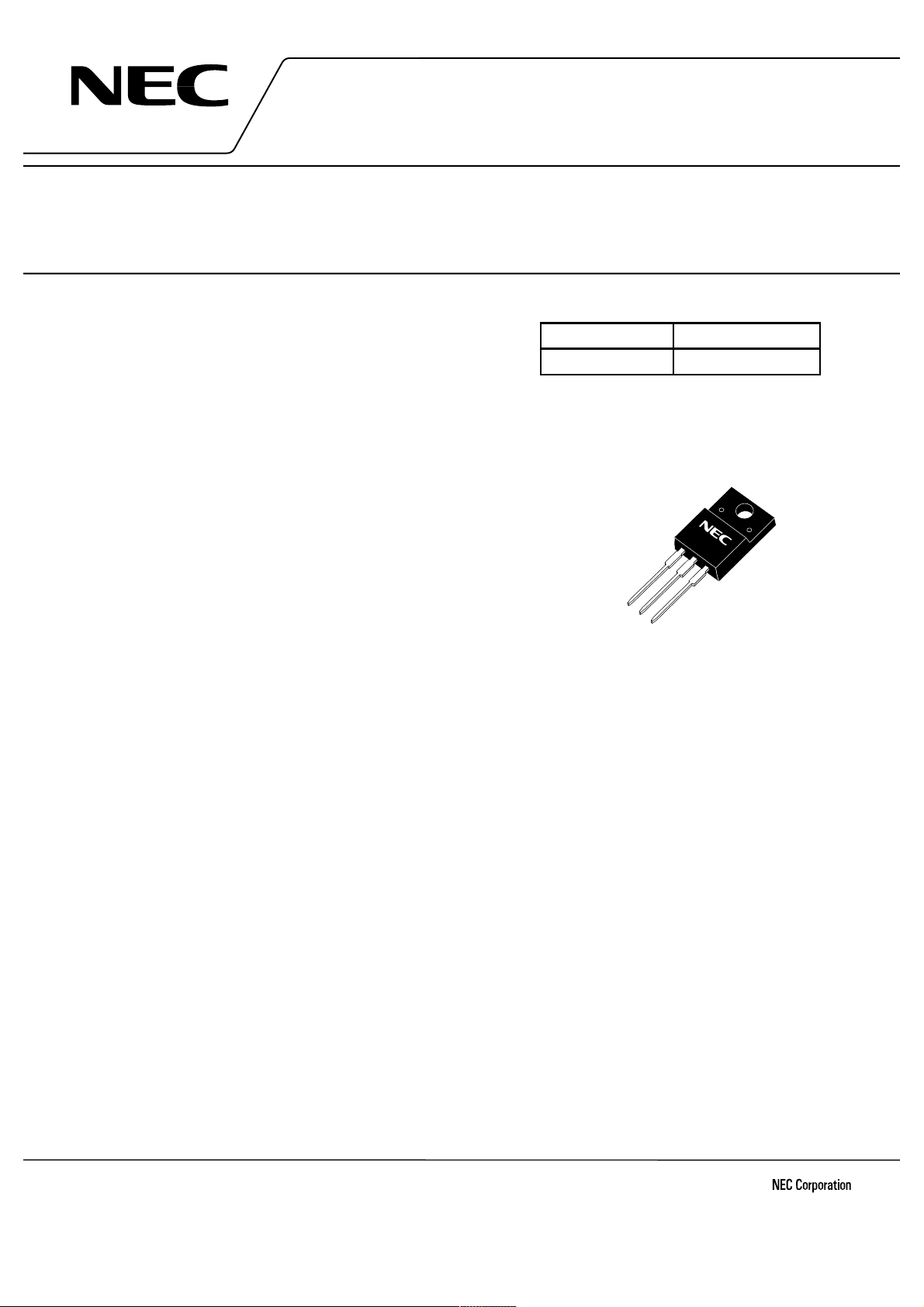
The 2SK3114 is N-channel DMOS FET device that features a
low gate charge and excellent switching characteristics, and
designed for high voltage applications such as switching power
supply, AC adapter.
FEATURES
•Low on-state resistance:
R
DS(on)
= 2.2
Ω MAX. (VGS
= 10 V, ID = 2.0 A)
•Low gate charge:
= 15 nC TYP. (VDD = 450 V, VGS = 10 V, ID = 4.0 A)
G
Q
•Gate voltage rating: ±30 V
•Avalanche capability ratings
•Isolated TO-220 package
ABSOLUTE MAXIMUM RATINGS (TA = 25°C)
GSS
D(DC)
D(pulse)
I
AS
I
E
DSS
T1
T2
ch
stg
AS
600 V
±30 V
±4.0 A
±16 A
30 W
2.0 W
150 °C
–55 to +150 °C
4.0 A
10.7 mJ
Drain to Source Voltage (VGS = 0 V) V
DS
Gate to Source Voltage (V
Drain Current (DC) (T
Drain Current (pulse)
Total Power Dissipation (T
Total Power Dissipation (T
Channel Temperature T
Storage Temperature T
Single Avalanche Current
Single Avalanche Energy
= 0 V) V
C
= 25°C) I
Note1
C
= 25°C) P
A
= 25°C) P
Note2
Note2
ORDERING INFORMATION
PART NUMBER PACKAGE
2SK3114 Isolated TO-220
★
(Isolated TO-220)
s, Duty cycle ≤ 1%
Notes 1. PW ≤ 10
2. Starting T
Document No. D13337EJ2V0DS00 (2nd edition)
Date Published January 2001 NS CP(K)
Printed in Japan
µ
= 25°C, VDD = 150 V, RG = 25 Ω, V
ch
The information in this document is subject to change without notice. Before using this document, please
confirm that this is the latest version.
Not all devices/types available in every country. Please check with local NEC representative for
availability and additional information.
= 20 → 0 V
GS
The mark ★ shows major revised points.
©
1998
Page 2
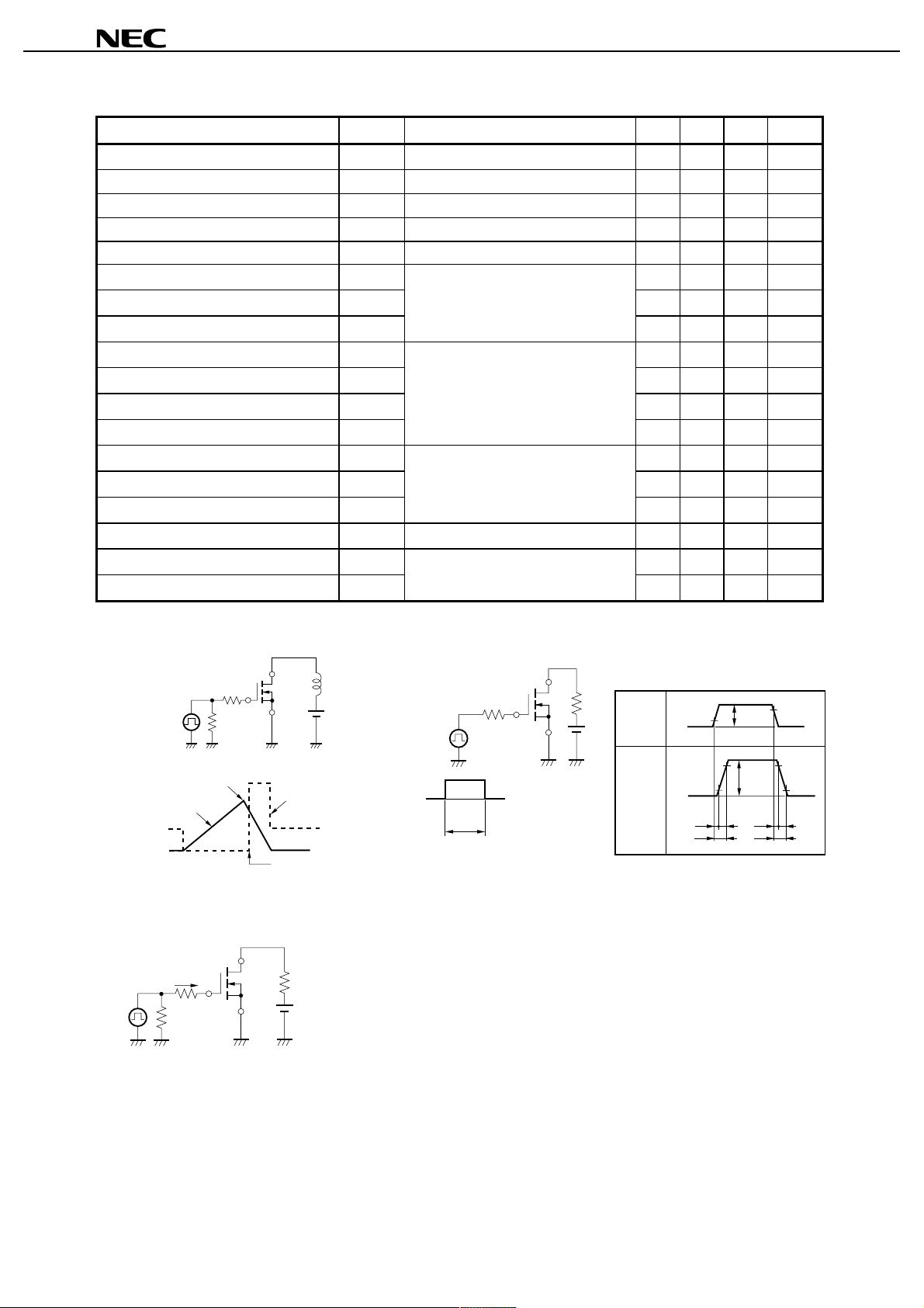
ELECTRICAL CHARACTERISTICS (TA = 25°C)
Characteristics Symbol Test Conditions MIN. TYP. MAX. Unit
2SK3114
Zero Gate Voltage Drain Current I
Gate Leakage Current I
Gate Cut-off Voltage V
DSS
VDS = 600
GSS
VGS = ±30 V, VDS = 0
GS(off)VDS
V, VGS = 0 V 100
V ±10
= 10 V, ID = 1 mA 2.5 3.5 V
A
µ
A
µ
Forward Transfer Admittance | yfs | VDS = 10 V, ID = 2.0 A1.050S
Drain to Source On-state Resistance R
Input Capacitance C
Output Capacitance C
Reverse Transfer Capacitance C
Turn-on Delay Time t
Rise Time t
Turn-off Delay Time t
Fall Time t
Total Gate Charge Q
Gate to Source Charge Q
Gate to Drain Charge Q
Body Diode Forward Voltage V
Reverse Recovery Time t
Reverse Recovery Charge Q
DS(on)VGS
iss
oss
rss
d(on)
r
d(off)
f
G
GS
GDID
F(S-D)IF
rr
rr
= 10 V, ID = 2.0
VDS = 10 V 550 pF
VGS = 0 V 115 pF
f = 1 MHz 13 pF
VDD = 150 V, ID = 2.0 A12ns
GS(on)
V
= 10 V6ns
RG = 10
Ω 35 ns
RL = 10
Ω 12 ns
VDD = 450 V15nC
VGS = 10 V4nC
= 4.0 A4.4nC
= 4.0 A, VGS = 0 V0.9V
IF = 4.0 A, VGS = 0 V1.3
di/dt = 50 A/µs4.3
A1.62.2Ω
s
µ
C
µ
TEST CIRCUIT 1 AVALANCHE CAPABILITY
D.U.T.
L
V
DD
PG.
RG = 25 Ω
50 Ω
VGS = 20 → 0 V
DSS
BV
I
AS
V
I
D
V
DD
DS
Starting T
ch
TEST CIRCUIT 3 GATE CHARGE
D.U.T.
PG.
IG = 2 mA
50 Ω
R
L
V
DD
TEST CIRCUIT 2 SWITCHING TIME
D.U.T.
L
R
R
PG.
V
GS
0
τ = 1 s
Duty Cycle ≤ 1%
G
V
DD
τ
µ
V
GS
Wave Form
I
D
Wave Form
V
GS
10%
0
I
90%
D
10%
0
t
d(on)
r
t
on
t
90%
V
GS
(on)
90%
I
D
10%
t
d(off)
t
f
t
off
2
Data Sheet D13337EJ2V0DS
Page 3
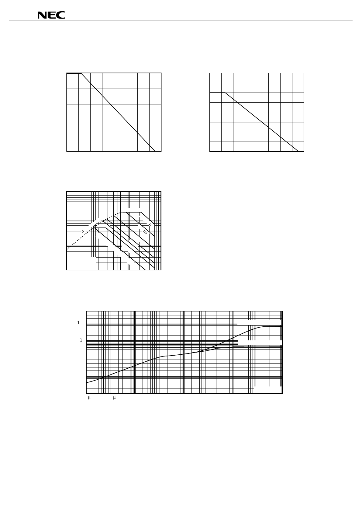
TYPICAL CHARACTERISTICS (TA = 25°C )
DERATING FACTOR OF FORWARD BIAS
SAFE OPERATING AREA
T
ch
- Channel Temperature -
˚C
dT - Percentage of Rated Power - %
04020 60 100 14080 120 160
100
80
60
40
20
0
TC - Case Temperature - ˚C
P
T
- Total Power Dissipation - W
08020 40 60 100 140120 160
40
30
20
10
TOTAL POWER DISSIPATION vs.
CASE TEMPERATURE
FORWARD BIAS SAFE OPERATING AREA
10 100 1 000
I
D
- Drain Current - A
1
V
DS
- Drain to Source Voltage - V
100
10
1
0.1
Power Dissipation Limited
100
m
s
10
ms
1
ms
100
m
s
PW
=
10
m
s
R
D
(on) Limited
ID(pulse)
ID(DC)
3
ms
TC = 25˚C
Single Pulse
2SK3114
100
10
1
0.1
0.01
10
m
rth(t) - Transient Thermal Resistance - ˚C/W
TRANSIENT THERMAL RESISTANCE vs. PULSE WIDTH
m
Data Sheet D13337EJ2V0DS
Rth(CH-A) = 62.5 ˚C/W
Rth(CH-C) = 4.17 ˚C/W
Single Pulse
100m 1 10 100 1 00010m1m100
PW - Pulse Width - s
3
Page 4
2SK3114
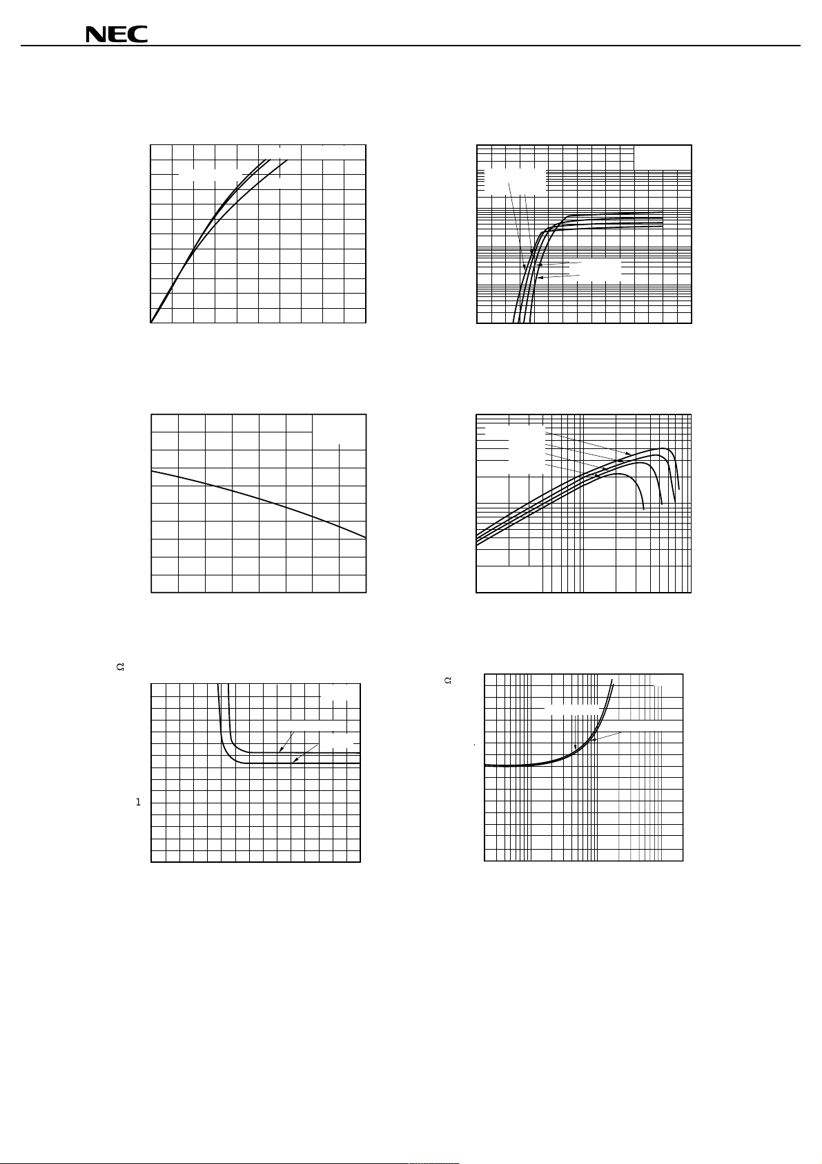
DRAIN CURRENT vs.
DRAIN TO SOURCE VOLTAGE
V
DS
- Drain to Source Voltage - V
I
D
- Drain Current - A
10 4020 30
5
10
0
6 V
VGS = 10 V
8 V
Pulsed
FORWARD TRANSFER CHARACTERISTICS
V
GS - Gate to Source Voltage - V
ID - Drain Current - A
151050
100
10
1.0
0.1
VDS = 10V
Pulsed
Tch = 125 ˚C
75 ˚C
25 ˚C
-25 ˚C
GATE TO SOURCE CUTOFF VOLTAGE
vs. CHANNEL TEMPERATURE
T
ch
- Channel Temperature -
˚C
V
GS(off)
- Gate to Source Cutoff Voltage - V
-50 0 50 100 150
5.0
4.0
3.0
2.0
1.0
0
VDS = 10 V
I
D
= 1 mA
FORWARD TRANSFER ADMITTANCE vs.
DRAIN CURRENT
1.0 10
I
D
- Drain Current - A
| y
fs
| - Forward Transfer Admittance - S
10
0.1
1.0
0.1
VDS = 10 V
Pulsed
Tch = -25 ˚C
25 ˚C
75 ˚C
125 ˚C
DRAIN TO SOURCE ON-STATE RESISTANCE vs.
GATE TO SOURCE VOLTAGE
10
2.0
V
GS
- Gate to Source Voltage - V
R
DS (on)
- Drain to Source On-State Resistance -
W
1.0
0
515
0
3.0
ID = 4.0 A
Pulsed
2.0 A
4
Data Sheet D13337EJ2V0DS
DRAIN TO SOURCE ON-STATE
RESISTANCE vs. DRAIN CURRENT
W
3.0
2.0
1.0
- Drain to Source On-State Resistance -
DS(on)
0
R
1.0
D
I
Pulsed
VGS = 10 V
VGS = 20 V
10 100
- Drain Current - A
Page 5
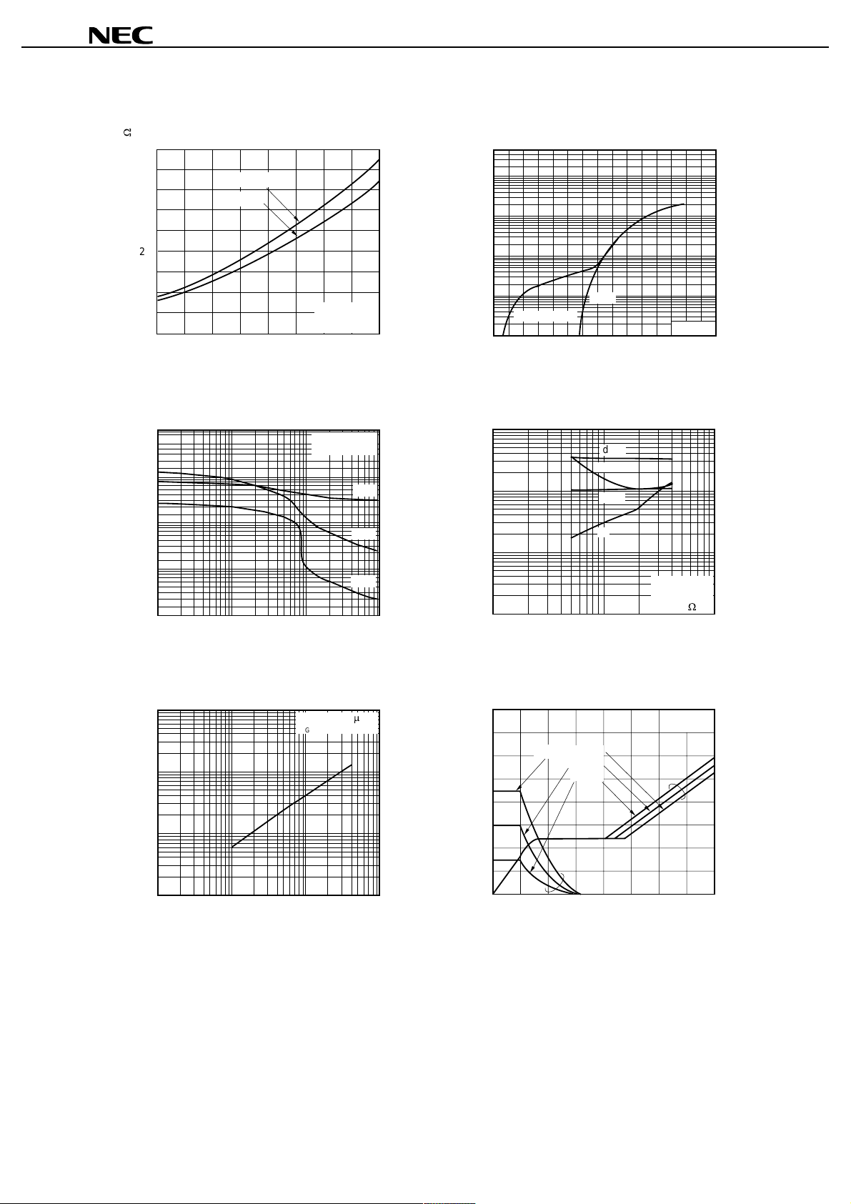
2SK3114
DRAIN TO SOURCE ON-STATE RESISTANCE vs.
CHANNEL TEMPERATURE
50 150
R
DS (on)
- Drain to Source On-State Resistance -
W
2.0
0
0 100-50
T
ch
- Channel Temperature -
˚C
3.0
1.0
VGS = 10 V
Pulsed
4.0
2.0 A
ID = 4.0 A
SOURCE TO DRAIN DIODE
FORWARD VOLTAGE
V
SD
- Source to Drain Voltage - V
I
SD
- Diode Forward Current - A
1.51.00.50
100
10
1.0
0.1
Pulsed
0 V
VGS = 10 V
1001010.1
10 000
CAPACITANCE vs. DRAIN TO
SOURCE VOLTAGE
C
iss
, C
oss
, C
rss
- Capacitance - pF
1 000
100
10
1
V
GS =
0 V
f = 1 MH
Z
C
iss
C
oss
C
rss
VDS - Drain to Source Voltage - V
SWITCHING CHARACTERISTICS
0.1 1 10
I
D
- Drain Current - A
td
(on)
,
tr,
td
(off)
,
tf
-
Switching
Time
-
ns
100
10
1
0.1
V
DD =
150 V
V
GS
= 10 V
RG = 10 W
td(off)
td(on)
tf
tr
REVERSE RECOVERY TIME vs.
DRAIN CURRENT
0.1 1 10
t
rr
- Reverse Recovery Time - ns
0.01
I
D
- Drain Current - A
10 000
1 000
100
10
di/dt = 50 A/
m
S
VGS = 0 V
Qg - Gate Charge - nC
V
DS
- Drain to Source Voltage - V
0841216
600
400
200
DYNAMIC INPUT/OUTPUT CHARACTERISTICS
V
GS
- Gate to Source Voltage - V
16
14
12
10
8
6
4
2
0
V
GS
V
DS
ID = 4 A
VDD = 450 V
300 V
150 V
Data Sheet D13337EJ2V0DS
5
Page 6
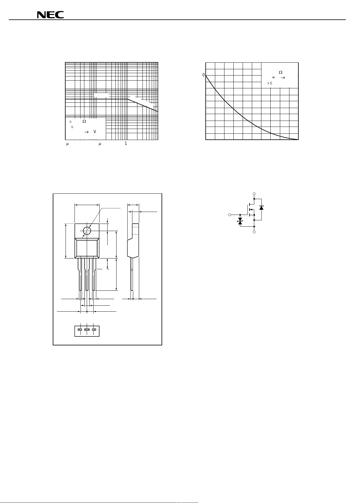
2SK3114
SINGLE AVALANCHE CURRENT vs.
INDUCTIVE LOAD
100
m
1m 10m
100
L - Inductive Load - H
I
AS
- Single Avalanche Current - A
1.0
10
0.1
10
m
RG = 25
W
V
DD
= 150 V
V
GS
= 20
®
0 V
Starting Tch = 25
˚C
E
AS
= 10.7 m
J
IAS = 4 A
SINGLE AVALANCHE ENERGY
DERATING FACTOR
75 150125
120
80
40
0
Starting Tch - Starting Channel Temperature - ˚C
Energy Derating Factor - %
50 10025
VDD =
150 V
R
G
= 25
W
V
GS
=
20 ®
0 V
I
AS
£ 4
A
100
60
20
PACKAGE DRAWINGS (Unit: mm)
Isolated TO-220 (MP-45F)
10.0±0.3
3.2±0.2
φ
3±0.1
15.0±0.3
4±0.2
0.7±0.1 1.3±0.2
1.5±0.2
2.54 TYP.2.54 TYP.
123
4.5±0.2
12.0±0.213.5 MIN.
0.65±0.1
1.Gate
2.Drain
3.Source
2.7±0.2
2.5±0.1
EQUIVALENT CIRCUIT
Drain
Body
Gate
Gate
Protection
Diode
Source
Diode
Remark
The diode connected between the gate and source of the transistor serves as a protector against ESD.
When this device actually used, an additional protection circuit is externally required if a voltage
exceeding the rated voltage may be applied to this device.
6
Data Sheet D13337EJ2V0DS
Page 7

[MEMO]
2SK3114
Data Sheet D13337EJ2V0DS
7
Page 8

2SK3114
•
The information in this document is current as of January, 2001. The information is subject to
change without notice. For actual design-in, refer to the latest publications of NEC's data sheets or
data books, etc., for the most up-to-date specifications of NEC semiconductor products. Not all
products and/or types are available in every country. Please check with an NEC sales representative
for availability and additional information.
•
No part of this document may be copied or reproduced in any form or by any means without prior
written consent of NEC. NEC assumes no responsibility for any errors that may appear in this docum e nt.
•
NEC does not assume any liability for infringement of patents, copyrights or other intellectual property rights of
third parties by or arising from the use of NEC semiconductor products listed in this document or any other
liability arising from the use of such products. No license, express, implied or otherwise, is granted under any
patents, copyrights or other intellectual property rights of NEC or others.
•
Descriptions of circuits, software and other related information in this document are provided for illustrative
purposes in semiconductor product operation and application examples. The incorporation of these
circuits, software and information in the design of customer's equipment shall be done under the full
responsibility of customer. NEC assumes no responsibility for any losses incurred by customers or third
parties arising from the use of these circuits, software and information.
•
While NEC endeavours to enhance the quality, reliability and safety of NEC semiconductor products, customers
agree and acknowledge that the possibility of defects thereof cannot be eliminated entirely. To minimize
risks of damage to property or injury (including death) to persons arising from defects in NEC
semiconductor products, customers must incorporate sufficient safety measures in their design, such as
redundancy, fire-containment, and anti-failure features.
•
NEC semiconductor products are classified into the following three quality grades:
"Standard", "Special" and "Specific". The "Specific" quality grade applies only to semiconductor products
developed based on a customer-designated "quality assurance program" for a specific application. The
recommended applications of a semiconductor product depend on its quality grade, as indicated below.
Customers must check the quality grade of each semiconductor product before using it in a particular
application.
"Standard": Computers, office equipment, communications equipment, test and measurement equipment, audio
and visual equipment, home electronic appliances, machine tools, personal electronic equipment
and industrial robots
"Spe c ial ": Transportation equipment (automobiles, trains, ships, etc.), traffic control systems, anti-disaster
systems, anti-crime systems, safety equipment and medical equipment (not specifically designed
for life support)
"Specific": Aircraft, aerospace equipment, submersible repeaters, nuclear reactor control systems, life
support systems and medical equipment for life support, etc.
The quality grade of NEC semiconductor products is "Standard" unless otherwise expressly specified in NEC's
data sheets or data books, etc. If c ustomers wish to use NEC semiconductor products in applications not
intended by NEC, they must contact an NEC sales representative in advance to determine NEC's willingness
to support a given application.
(Note)
(1) "NEC" as used in this statement means NEC Corporation and also includes its majority-owned subsidiaries.
(2) "NEC semiconductor products" means any semiconductor product developed or manufactured by or for
NEC (as defined above).
M8E 00. 4
 Loading...