DATA SHEET
2.0 ±0.2
0.65 0.65
2.1 ±0.1
0.15
+0.1
–0.05
0.3
0.9 ±0.1
0.3
+0.1
–0
0.3
+0.1
–0
2
1
3
1.25 ±0.1
Marking
0 to 1.1
MOS FIELD EFFECT TRANSISTOR
2SJ463A
P-CHANNEL MOS FIELD EFFECT TRANSISTOR
FOR HIGH SPEED SWITCHING
DESCRIPTION
The 2SJ463A is a switching device which can be driven directly
by a 2.5 V power source.
The 2SJ463A has excellent switching characteristics, and is
suitable for use as a high-speed switching device in digital circuits.
FEATURES
• Can be driven by a 2.5 V power source.
• Low Gate Cut-off Voltage.
ABSOLUTE MAXIMUM RATINGS (TA = 25 °C)
Drain to Source Voltage VDSS –30 V
Gate to Source Voltage V
Drain Current (DC) ID(DC) +0.1 A
Drain Current (pulse) ID(pulse) +0.4
Total Power Dissipation P
Channel Temperature Tch 150 °C
Storage Temperature Tstg –55 to +150 °C
µ
Note PW ≤ 10
s, Duty Cycle ≤ 1 %
GSS +20 V
Note
T 150 mW
A
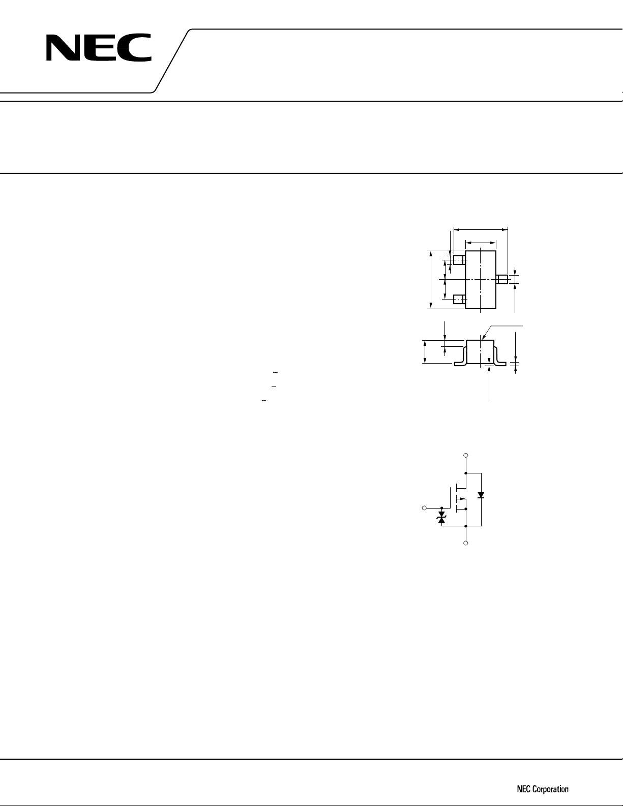
Package Drawings (unit: mm)
Equivalent Circuit
Drain
Gate
Electrode
Connection
1. Source
2. Gate
3. Drain
Internal Diode
Document No. D11198EJ1V0DS00 (1st edition)
Date Published September 1996 P
Printed in Japan
The diode connected between the gate and source of the transistor serves as a protector against ESD. When this
device is actually used, an additional protection circuit is externally required if a voltage exceeding the rated voltage
may be applied to this device.
Gate Protect
Diode
Source
Marking : H21
©
1996

ELECTRICAL CHARACTERISTICS (TA = 25 ˚C)
CHARACTERISTIC SYMBOL MIN. TYP. MAX. UNIT TEST CONDITIONS
Drain Cut-off Current IDSS –1
Gate Leakage Current IGSS +10
Gate Cut-off Voltage VGS(off) –1.0 –1.4 –1.7 V VDS = –3 V, ID = –10 µA
Forward Transfer Admittance | y fs |20 mSVDS = –3 V, ID = –10 mA
Drain to Source On-State RDS(on)1 23 60 Ω VGS = –2.5 V, ID = –1 mA
Resistance
Drain to Source On-State RDS(on)2 11 23 Ω VGS = –4 V, ID = –10 mA
Resistance
Drain to Source On-State RDS(on)3 613ΩVGS = –10 V, ID = –10 mA
Resistance
Input Capacitance Ciss 5pFVDS = –3 V
Output Capacitance Coss 15 pF VGS = 0
Reverse Transfer Capacitance Crss 1.3 pF f = 1 MHz
Turn-on Delay Time td(on) 140 ns VDD = –3 V, ID = –10 mA
Rise Time tr 330 ns VGS(on) = –4 V, RG = 10 Ω
Turn-off Delay Time td(off) 220 ns RL = 300 Ω
Fall Time tf 320 ns
µ
AVDS = –30 V, VGS = 0
µ
AVGS = +20 V, VDS = 0
2SJ463A
2

2SJ463A
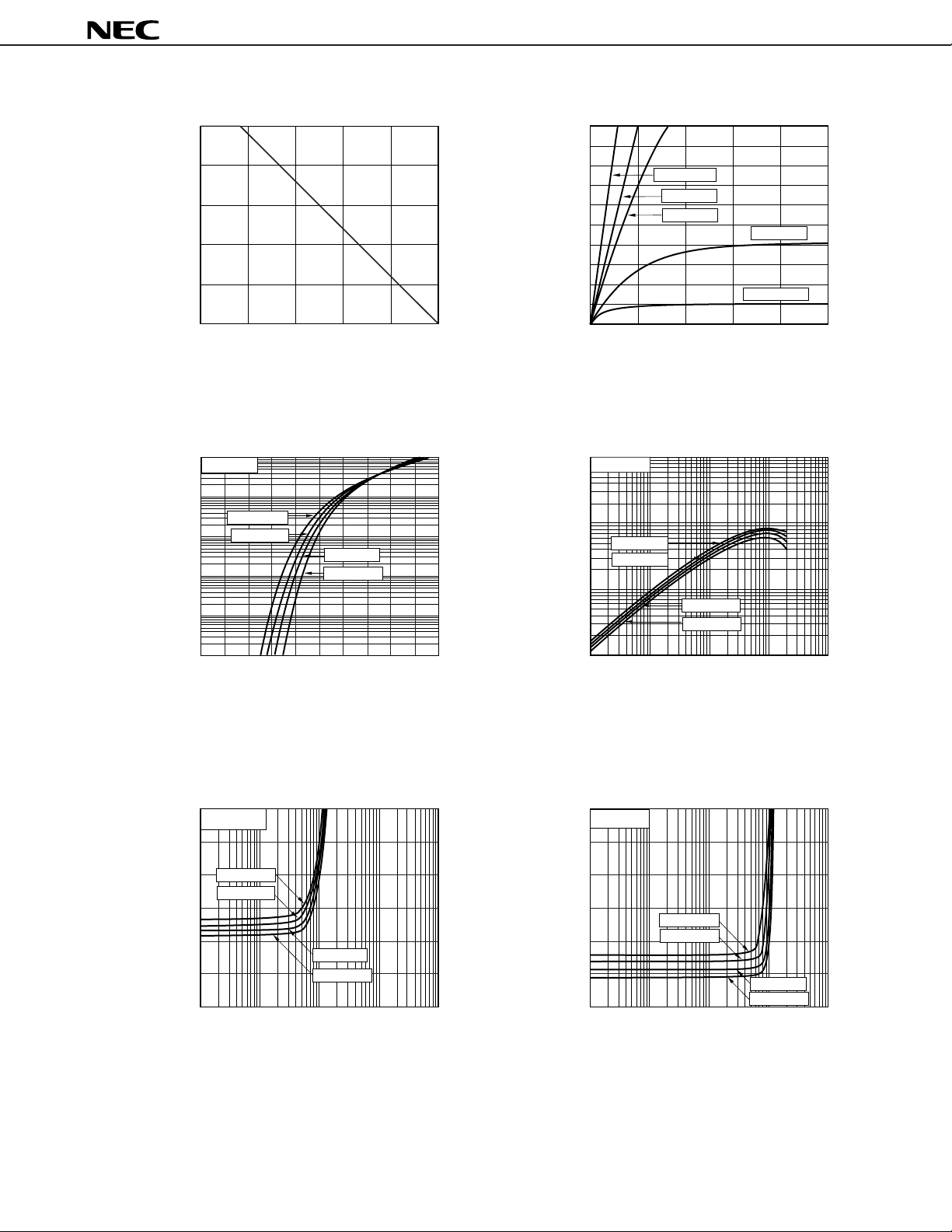
DERATING FACTOR OF FORWARD BIAS
SAFE OPERATING AREA
100
80
60
40
dT - Derating Factor - %
20
0
0 30 60 90 120 150
T
A
- Ambient Temperature - °C
TRANSFER CHARACTERISTICS
–100
V
DS
= –3 V
–10
TA = 125 °C
–1
TA = 75 °C
TA = 25 °C
–0.1
- Drain Current - mA
D
I
–0.01
TA = –25 °C
–0.001
0 –0.8 –1.6 –2.4 –3.2 –4.0
V
GS
- Gate to Source Voltage - V
DRAIN CURRENT vs.
DRAIN TO SOURCE VOLTAGE
–100
–80
–60
–40
- Drain Current - mA
D
I
–20
0
0 –1 –2 –3 –4 –5
V
GS
= –10 V
V
GS
= –6 V
V
GS
= –4 V
V
DS
- Drain to Source Voltage - V
V
V
GS
GS
= –3 V
= –2.5 V
FORWARD TRANSFER ADMITTANCE vs.
DRAIN CURRENT
1000
V
DS
= –3 V
100
TA = –25 °C
TA = 25 °C
10
TA = 75 °C
TA = 125 °C
I - Forward Transfer Admittance - mS
fs
Iy
1
–0.1 –1 –10 –100 –1000
D
- Drain Current - mA
I
DRAIN TO SOURCE ON-STATE RESISTANCE vs.
DRAIN CURRENT
60
V
GS
= –2.5 V
50
40
TA = 125 °C
TA = 75 °C
30
20
TA = 25 °C
10
- Drain to Source On-State Resistance - Ω
0
DS(on)
–0.1 –1 –10 –100 –1000
R
TA = –25 °C
ID - Drain Current - mA
DRAIN TO SOURCE ON-STATE RESISTANCE vs.
DRAIN CURRENT
60
V
GS
= –4 V
50
40
30
TA = 125 °C
20
TA = 75 °C
10
- Drain to Source On-State Resistance - Ω
0
DS(on)
–0.1 –1 –10 –100 –1000
R
I
D
- Drain Current - mA
TA = 25 °C
TA = –25 °C
3
 Loading...