DATA SHEET
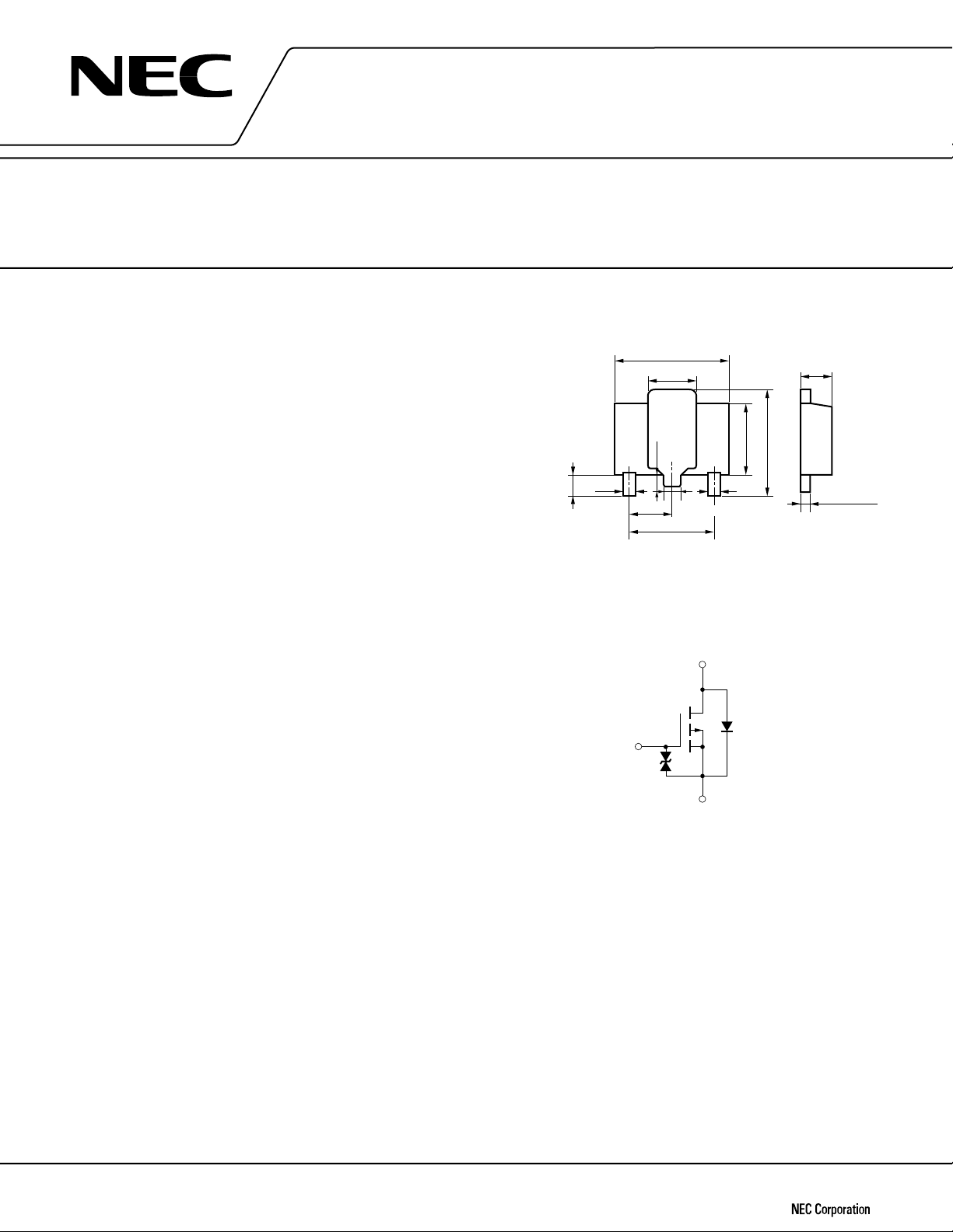
5.7 ±0.1
2.0 ±0.2
213
1.5 ±0.1
0.4 ±0.05
4.2
0.85 ±0.1
2.1
0.5 ±0.1
1.0
0.55
0.5 ±0.1
3.65 ±0.1
5.4 ±0.25
MOS FIELD EFFECT TRANSISTOR
2SJ462
P-CHANNEL MOS FIELD EFFECT TRANSISTOR
FOR HIGH SPEED SWITCHING
DESCRIPTION
The 2SJ462 is a switching device which can be driven directly
by an IC operating at 3 V.
The 2SJ462 features a low on-state resistance and can be
driven by a low voltage power source, so it is suitable for applications such as power management.
FEATURES
• Can be driven by a 2.5 V power source.
• New-type compact package.
Has advantages of packages for small signals and for power
transistors, and compensates those disadvantages.
• Low on-state resistance.
DS(ON) : 0.29 Ω MAX. @VGS = –2.5 V, ID = –0.5 A
R
RDS(ON) : 0.19 Ω MAX. @VGS = –4.0 V, ID = –1.0 A
ABSOLUTE MAXIMUM RATINGS (TA = +25 ˚C)
Drain to Source Voltage VDSS –12 V
Gate to Source Voltage V
Drain Current (DC) ID(DC) ±2.5 A
Drain Current (pulse) ID(pulse) ±5.0* A
Total Power Dissipation P
Channel Temperature Tch 150 ˚C
Storage Temperature Tstg –55 to +150 ˚C
* PW ≤ 10 ms, Duty Cycle ≤ 1 %
** Mounted on ceramic board of 7.5 cm
GSS ±8.0 V
T 2.0** W
2
× 0.7 mm
Package Drawings (unit : mm)
Equivalent Circuit
Electrode
Connection
1. Source
2. Drain
3. Gate
Internal Diode
Gate
Gate Protect
Diode
Drain
Source
Marking : UA3
Document No. D11449EJ1V0DS00 (1st edition)
Date Published April 1996 P
Printed in Japan
©
1996

ELECTRICAL SPECIFICATIONS (TA = +25 ˚C)
Parameter Symbol MIN. TYP. MAX. Unit Conditions
Drain Cut-off Current IDSS –10
Gate Leakage Current IGSS ±10
Gate Cut-off Voltage VGS(off) –0.7 –1.0 –1.3 V VDS = –3.0 V, ID = –1.0 mA
Forward Transfer Admittance |yfs| 1.5 S VDS = –3.0 V, ID = –1.0 A
Drain to Source On-State RDS(on)1 195 290 mΩ VGS = –2.5 V, ID = –0.5 A
Resistance
Drain to Source On-State RDS(on)2 135 190 mΩ VGS = –4.0, ID = –1.0 A
Resistance
Input Capacitance Ciss 940 pF VDS = –3.0 V, VGS = 0
Output Capacitance Coss 835 pF f = 1.0 MHz
Reverse Transfer Capacitance Crss 495 pF
Turn-On Delay Time td(on) 45 ns VDD = –3.0 V, ID = –1.0 A
Rise Time tr 225 ns
Turn-Off Delay Time td(off) 140 ns
Fall Time tf 195 ns
Total Gate Charge QG 12 nC VDS = –8 V, ID = –2.5 A
Gate to Source Charge QGS 2nC
Gate to Drain Charge QGD 7nC
Diode Forward Voltage VF(S–D) –0.86 V IF = –2.5 A, VGS = 0
Reverse Recovery Time trr 150 ns IF = –2.5 A, VGS = 0
Reverse Recovery Charge Qrr 160 nC
µ
AVDS = –12 V, VGS = 0
µ
AVGS = ±8.0 V, VDS = 0
VGS(on) = –3.0 V, RG = 10 Ω
RL = 3.0 Ω
VGS = –3.0 V, IG = –2 mA
di/dt = 50 A/µs
2SJ462
2
 Loading...