

Page 1
DATA SHEET
MOS FIELD EFFECT TRANSISTOR
2SJ358
P-CHANNEL MOS FET FOR HIGH-SPEED SWITCH
The 2SJ358 is a P-channel vertical MOS FET that can
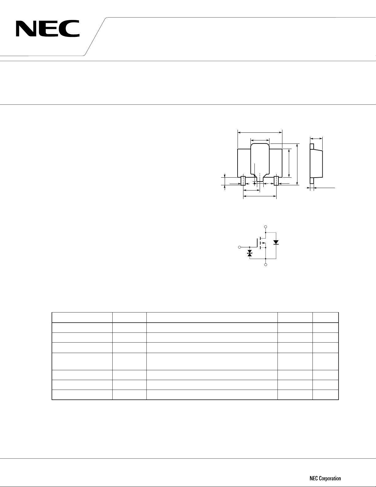
Package Drawings (unit: mm)
be used as a switching element. The 2SJ358 can be
directly driven by an IC operating at 5 V.
5.7 ±0.1
2.0 ±0.2
1.5 ±0.1
The 2SJ358 features a low on-resistance and excellent
switching characteristics, and is suitable for applications
such as actuator driver and DC/DC converter.
FEATURES
• New-type compact package
Has advantages of packages for small signals and for
0.5 ±0.1
1.0
2.1
0.55
4.2
231
0.85 ±0.1
3.65 ±0.1
0.5 ±0.1
5.4 ±0.25
power transistors, and compensates those disadvan-
tages
• Can be directly driven by an IC operating at 5 V.
• Low on-resistance
RDS(ON) = 0.40 Ω MAX. @VGS = –4 V, ID = –1.5 A
R
DS(ON) = 0.30 Ω MAX. @VGS = –10 V, ID = –1.5 A
QUALITY GRADE
Standard
Please refer to "Quality grade on NEC Semiconductor Devices" (Document number IEI-1209) published by
NEC Corporation to know the specification of quality grade on the devices and its recommended applications.
Equivalent Circuit
Drain (D)
Gate (G)
Gate Protect
Diode
Source (S)
Internal
Diode
Electrode Connection
1. Source
2. Drain
3. Gate
Marking: UA2
0.4 ±0.05
ABSOLUTE MAXIMUM RATINGS (Ta = +25 ˚C)
Parameter Symbol Conditions Ratings Unit
Drain-Source Voltage VDSS VGS = 0 –60 V
Gate-Source Voltage VGSS VDS = 0 –20/+10 V
Drain Current (DC) ID(DC) –/+3.0 A
Drain Current (Pulse) ID(pulse) PW ≤ 10 ms –/+6.0 A
Total Power Loss P
Channel Temperature Tch 150 ˚C
Storage Temperature Tstg –55 to +150 ˚C
The diode connected between the gate and source of the transistor serves as a protector against ESD. When
this device is actually used, an additional protection circuit is externally required if a voltage exceeding the
rated voltage may be applied to this device.
Document No. TC-2491
(O.D. No. TC-8011)
Date Published October 1994 P
Printed in Japan
Duty Cycle ≤ 1 %
T
The information in this document is subject to change without notice.
Mounted on ceramic board of 7.5 cm
2
× 0.7 mm 2.0 W
©
1994
Page 2
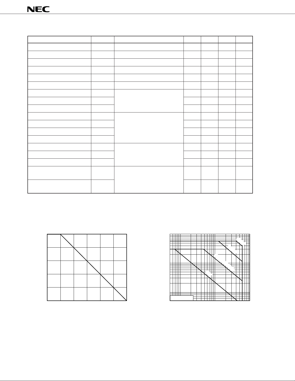
ELECTRICAL SPECIFICATIONS (Ta = +25 ˚C)
Parameter Symbol Conditions MIN. TYP. MAX. Unit
Drain Shut-down Current IDSS VDS = –60 V, VGS = 0 –10
Gate Leak Current IGSS VGS = –16/+10 V, VDS = 0 –/+10
Gate Cutoff Voltage VGS(off) VDS = –10 V, ID = –1 mA –1.0 –1.4 –2.0 V
Forward Transfer Admittance
Drain-Source On-Resistance RDS(on)1 VGS = –4 V, ID = –1.5 A 0.29 0.40 Ω
Drain-Source On-Resistance RDS(on)2 VGS = –10 V, ID = –1.5 A 0.18 0.30 Ω
Input Capacitance Ciss VDS = –10 V, VGS = 0, 600 pF
Output Capacitance Coss
Feedback Capacitance Crss 120 pF
On-Time Delay td(on) VDD = –25 V, ID = –1.5 A 6 ns
Rise Time tr
Off-Time Delay td(off)
Fall Time tf 95 ns
Gate Input Charge QG VDS = –48 V, 23.9 nC
Gate-Source Chanrge QGS
Gate-Drain Charge QGD
Internal Diode Reverse trr IF = 3.0 A 95 ns
Recovery Time di/dt = 50 A/µs
Internal Diode Reverse Qrr 118 nC
Recovery Charge
|yfs| VDS = –10 V, ID = –1.0 A 1.8 S
f = 1.0 MHz
V
= –10 V
GS(on)
R
= 10 Ω, RL = 17 Ω
G
VGS = –10 V,
ID = –3.1 A, IG = –2 mA
300 pF
35 ns
155 ns
1.5 nC
8.1 nC
2SJ358
µ
A
µ
A
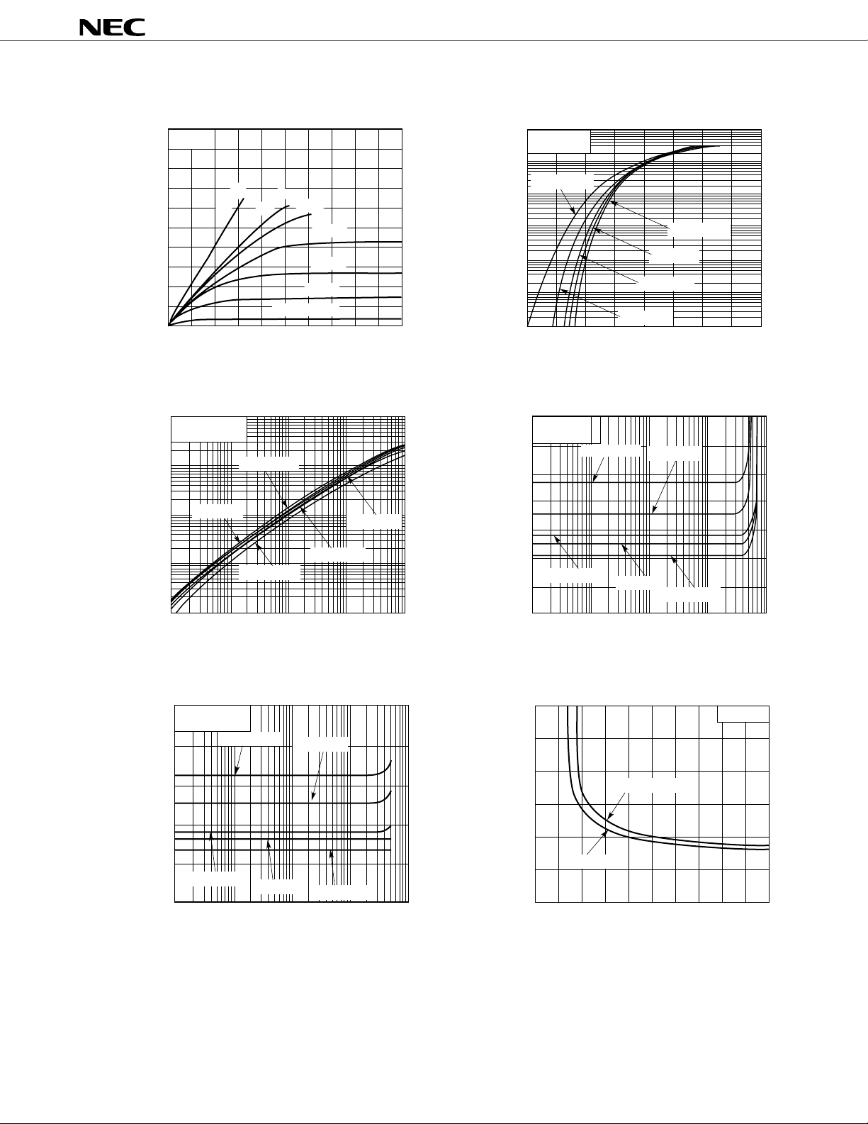
CHARACTERISTICS CURVES (Ta = +25 ˚C)
DERATING FACTOR OF FORWARD BIAS
SAFE OPERATING AREA
100
80
60
40
dT – Derating Factor – %
20
25
0 50 75 100 125 150
a – Ambient Temperature – ˚C
T
FORWARD BIAS SAFE OPERATING AREA
–10
–5
–2
–1
–0.5
ID – Drain Current – A
–0.2
–0.1
Single Pulse
–0.05
–1
–0.5 –2 –5 –10 –20 –100
DS – Drain to Source Voltage – V
V
DS
10 ms
PW = 100 ms
1 ms
–50
2
Page 3
2SJ358
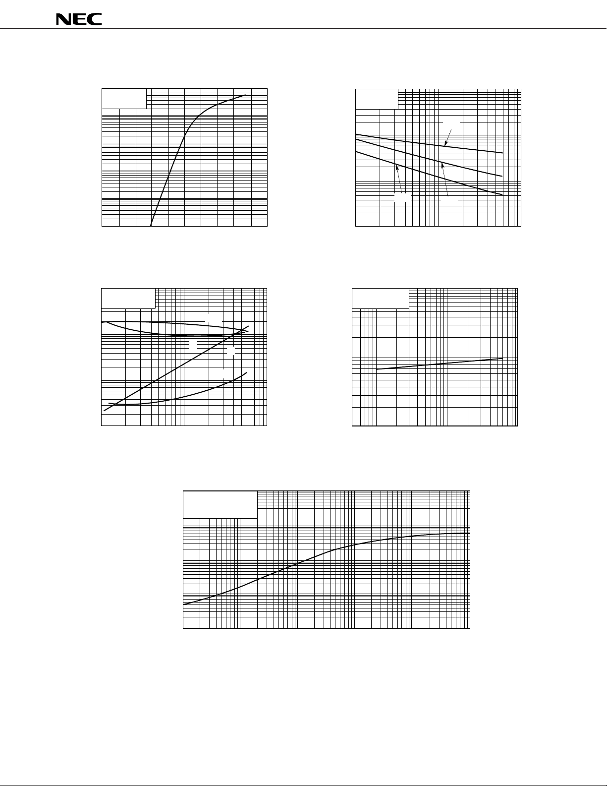
DRAIN CURRENT vs.
DRAIN TO SOURCE VOLTAGE
–10
Pulsed
–8
–6
–10 V
–4.5 V
–4.0 V
–3.5 V
–4
= –2.0 V
GS
V
–3.0 V
–2.5 V
ID – Drain Current – A
–2
0–2–3–4–5
–1
DS – Drain to Source Voltage – V
V
FORWARD TRANSFER ADMITTANCE vs.
DRAIN CURRENT
10
VDS = –10 V
Pulsed
Ta = –25 ˚C
Ta = 25 ˚C
0.1
1
Ta = 0 ˚C
–10
VDS = –10 V
Pulsed
–1
Ta = 150 ˚C
–0.1
–0.01
–0.001
ID – Drain Current –A
–0.0001
–0.00001
–1
DRAIN TO SOURCE ON-STATE RESISTANCE vs.
DRAIN CURRINT
0.7
V
GS = –4 V
Pulsed
0.6
0.5
0.4
0.3
TRANSFER CHARACTERISTICS
Ta = –25 ˚C
Ta = 0 ˚C
Ta = 25 ˚C
Ta = 75 ˚C
–2 –3
GS – Gate to Source Voltage – V
V
Ta = 150 ˚C
Ta = 75 ˚C
–4
0.01
Ta = 150 ˚C
Ta = 75 ˚C
|yfs| – Forward Transfer Admittence – S
0.001
–0.0001
–0.001
I
–0.01 –0.1 –1
D – Drain Current – A
DRAIN TO SOURCE ON-STATE RESISTANCE vs.
DRAIN CURRENT
0.5
V
GS = –10 V
Pulsed
0.4
Ta = 150 ˚C
Ta = 75 ˚C
0.3
0.2
0.1
RDS(on) – Drain to Source On-State Resistance – Ω
0
–0.001
Ta = 25 ˚C
Ta = 0 ˚C
–0.01
I
D – Drain Current – A
–0.1 –1 –10
Ta = –25 ˚C
0.2
Ta = 25 ˚C
0.1
0
–0.01
RDS(on) – Drain to Source On-State Resistance – Ω
–0.01 –0.1
Ta = 0 ˚C
Ta = –25 ˚C
D – Drain Current – A
I
DRAIN TO SOURCE ON-STATE RESISTANCE vs.
GATE TO SOURCE VOLTAGE
0.6
0.4
ID = 3.0 A
0.2
ID = 1.5 A
–2
0
RDS(on) – Drain to Source On-State Resistance – Ω
–4 –6 –8 –10 –12 –14 –16 –18 –20
V
GS – Gate to Source Voltage – V
–1
–10
Pulsed
3
Page 4
2SJ358
SOURCE TO DRAIN DIODE
FORWARD VOLTAGE
–10
VGS = 0
Pulsed
–1
–0.1
–0.01
–0.001
ISD – Diode Forward Current – A
–0.0001
–0.2
1000
100
10
–0.4 –0.6 –0.8 –1.0 –1.2
SD – Source to Drain Voltage – V
V
SWITCHING CHARACTERISTICS
VDD = –25 V
VGS(ON) = –10 V
CAPACITANCE vs.
DRAIN TO SOURCE VOLTAGE
10000
Ciss, Coss, Crss – Capacitance – pF
td(off)
tf
tr
td(on)
1000
100
10
1000
100
VGS = 0
f = 1 MHz
Crss
–1
VDS – Drain to Source Voltage – V
REVERSE RECOVERY TIME vs.
DIODE FORWARD CURRENT
VGS = 0
di/dt = 50 A/ s
µ
–10 –100
Ciss
Coss
td(on), tr, td(off), tr – Switching Time – ns
0.1
110
ID – Drain Current – A
1000
Single Pulse
Using ceramic board
of 7.5 cm
100
10
1
0.1
1 m
rth(j–a) – Transient Thermal Resistance – ˚C/W
trr – Reverse Recovery Time – ns
10
–0.1 –0.5 –5
–0.05
ID – Diode Forward Current – A
TRANSIENT THERMAL RESISTANCE vs. PULSE WIDTH
2
× 0.7 mm
10 m 1
100 m
PW – Pulse Width – s
10 100
–1 –10
4
Page 5
RELATED DOCUMENTS
Document Name Document No.
Semiconductor Device Mounting Technology Manual IEI-1207
NEC Semiconductor Device Reliability/Quality Control System TEI-1202
Guide to Quality Assurance for Semiconductor Device MEI-1202
2SJ358
5
Page 6

[MEMO]
2SJ358
No part of this document may be copied or reproduced in any form or by any means without the prior written
consent of NEC Corporation. NEC Corporation assumes no responsibility for any errors which may appear in this
document.
NEC Corporation does not assume any liability for infringement of patents, copyrights or other intellectual
property rights of third parties by or arising from use of a device described herein or any other liability arising
from use of such device. No license, either express, implied or otherwise, is granted under any patents,
copyrights or other intellectual property rights of NEC Corporation or others.
The devices listed in this document are not suitable for use in aerospace equipment, submarine cables, nuclear
reactor control systems and life support systems. If customers intend to use NEC devices for above applications
or they intend to use "Standard" quality grade NEC devices for applications not intended by NEC, please contact
our sales people in advance.
Application examples recommended by NEC Corporation
Standard:Computer, Office equipment, Communication equipment, Test and Measurement equipment,
Machine tools, Industrial robots, Audio and Visual equipment, Other consumer products, etc.
Special: Automotive and Transportation equipment, Traffic control systems, Antidisaster systems, Anticrime
systems, etc.
M4 92.6
 Loading...