

Page 1
DATA SHEET
NPN SILICON RF TRANSISTOR
NPN SILICON RF TRANSISTOR FOR
MEDIUM OUTPUT POWER AMPLIFICATION (0.4 W)
FLAT-LEAD 4-PIN THIN-TYPE SUPER MINIMOLD (M04)
FEATURES
• Ideal for 460 MHz to 2.4 GHz medium output power amplification
O (1 dB)
•P
• High collector efficiency:
• UHS0-HV technology (fT = 25 GHz) adopted
• High reliability through use of gold electrodes
• Flat-lead 4-pin thin-type super minimold (M04) package
ORDERING INFORMATION
= 26.0 dBm TYP. @ VCE = 3.6 V, f = 1.8 GHz, Pin = 15 dBm
C
= 60%
η
2SC5754
Part Number Quantity Supplying Form
2SC5754 50 pcs (Non reel) • 8 mm wide embossed taping
2SC5754-T2 3 kpcs/reel • Pin 1 (Emitter), Pin 2 (Col l ector) face the perforation si de of the tape
Remark
To order evaluation samples, contact your nearby sales office.
The unit sample quantity is 50 pcs.
Caution Observe precautions when handling because these devices are sensitive to electrostatic discharge.
The information in this document is subject to change without notice. Before using this document, please confirm that
this is the latest version.
Not all devices/types available in every country. Please check with local NEC Compound Semiconductor Devices
representative for availability and additional information.
Document No. PU10008EJ02V0DS (2nd edition)
Date Published March 2003 CP(K)
Printed in Japan
The mark
••••
shows major revised points.
NEC Compound Semiconductor Devices 2001, 2003
Page 2
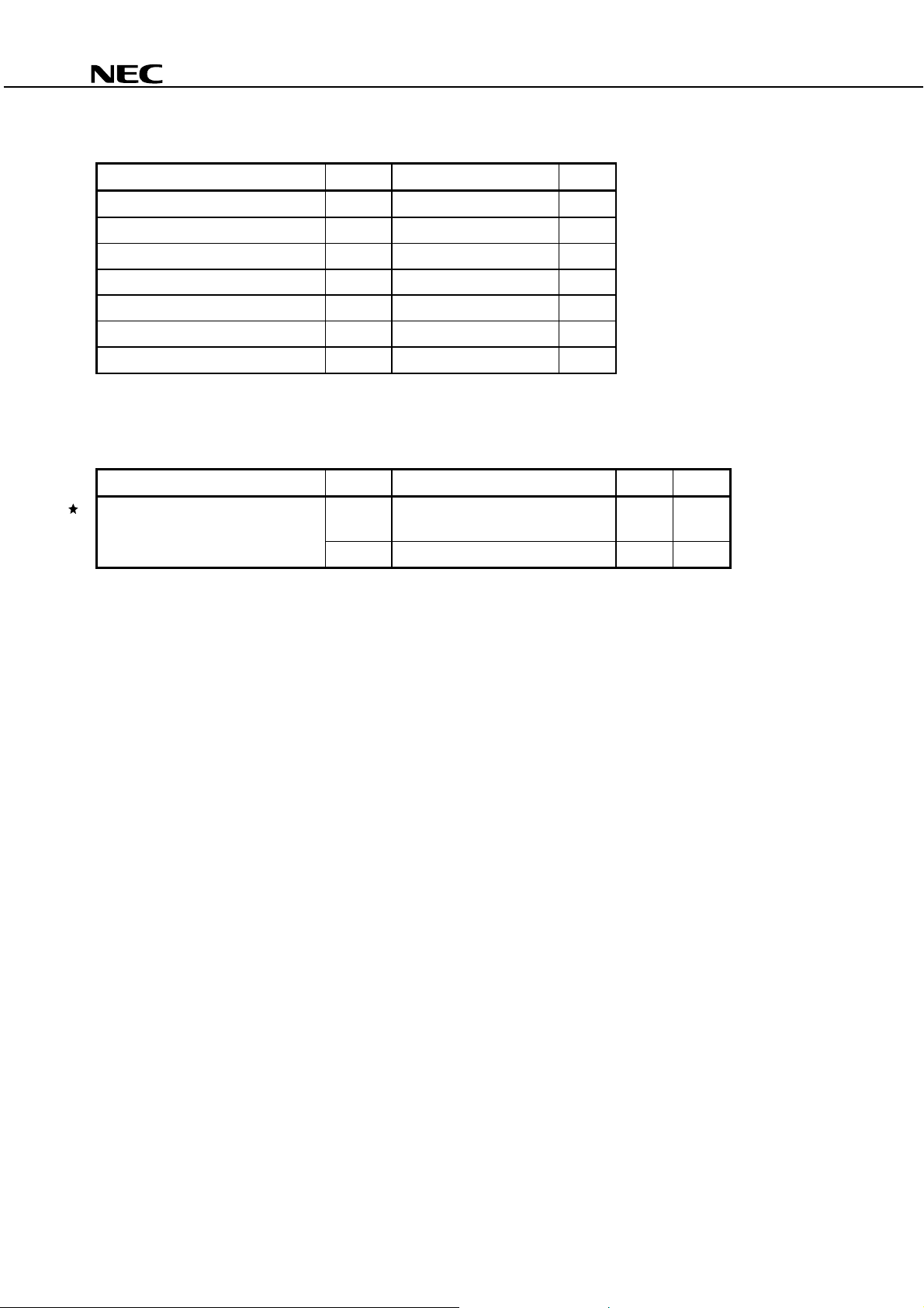
ABSOLUTE MAXIMUM RATINGS (TA = +25°°°°C)
Parameter Symbol Ratings Unit
2SC5754
Collector to Base Voltage V
Collector to Emitter Voltage V
Emitter to Base Voltage V
Collector Current I
Total Power Dissipation
Junction Temperature T
Storage Temperature T
Mounted on 38 × 38 mm, t = 0.4 mm polyimide PCB
Note
THERMAL RESISTANCE
Parameter Symbol Test Conditions Ratings Unit
Junction to Ambient Resistance R
CBO
CEO
EBO
C
Note
tot
P
j
stg
th j-a
1 Mounted on 38 × 38 mm, t = 0.4 mm
13 V
5.0 V
1.5 V
500 mA
735 mW
150
−
65 to +150
°
C
°
C
polyimide PCB
th j-a
R
2 Stand alone device in free air 570
170
°
C/W
°
C/W
2
Data Sheet PU10008EJ02V0DS
Page 3
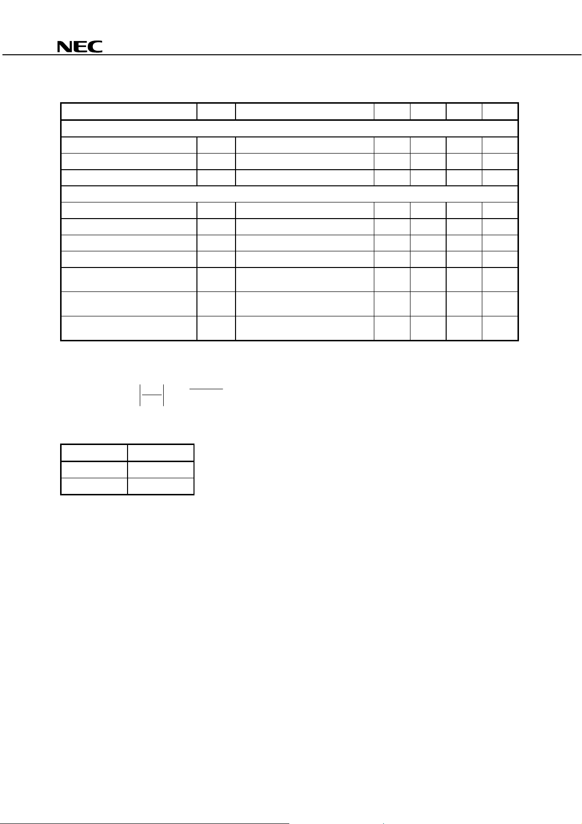
ELECTRICAL CHARACTERISTICS (TA = +25°°°°C)
Parameter Symbol Test Conditions MIN. TYP. MAX. Unit
DC Characteristics
FE
h
S
re
C
MAG
O (1 dB)
CBO
VCB = 5 V, IE = 0 mA
EBO
VBE = 1 V, IC = 0 mA
Note 1
VCE = 3 V, IC = 100 mA 40 60 100
T
VCE = 3 V, IC = 100 mA, f = 0.5 GHz 16 20
2
21e
VCE = 3 V, IC = 100 mA, f = 2 GHz 5.0 6.5
Note 2
VCB = 3 V, IE = 0 mA, f = 1 MHz
Note 3
VCE = 3 V, IC = 100 mA, f = 2 GHz
VCE = 3.6 V, ICq = 20 mA, f = 1.8 GHz,
L
in
P
= 0 dBm, 1/2 Duty
VCE = 3.6 V, ICq = 4 mA, f = 1.8 GHz,
in
P
= 15 dBm, 1/2 Duty
VCE = 3.6 V, ICq = 4 mA, f = 1.8 GHz,
η
C
in
P
= 15 dBm, 1/2 Duty
Collector Cut-off Current I
Emitter Cut-off Current I
DC Current Gain
RF Characteristics
Gain Bandwidth Product f
Insertion Power Gain
Reverse Transfer Capacitance
Maximum Available Power Gain
Linear Gain G
Gain 1 dB Compression Output Power P
Collector Efficiency
−−
−−
−
−
−
−
−
1.0 1.5 pF
12.0
12.0
26.0
60
2SC5754
1 000 nA
1 000 nA
−
−
−
−
−
−
GHz
dB
dB
dB
dBm
%
−
Notes 1.
Pulse measurement: PW ≤ 350
Collector to base capacitance when the emitter grounded
2.
21
3.
MAG =
S
12
S
hFE CLASSIFICATION
Rank FB
Marking R57
hFE Value 40 to 100
(K –
(K2 – 1) )
√√√√
s, Duty Cycle ≤ 2%
µ
Data Sheet PU10008EJ02V0DS
3
Page 4
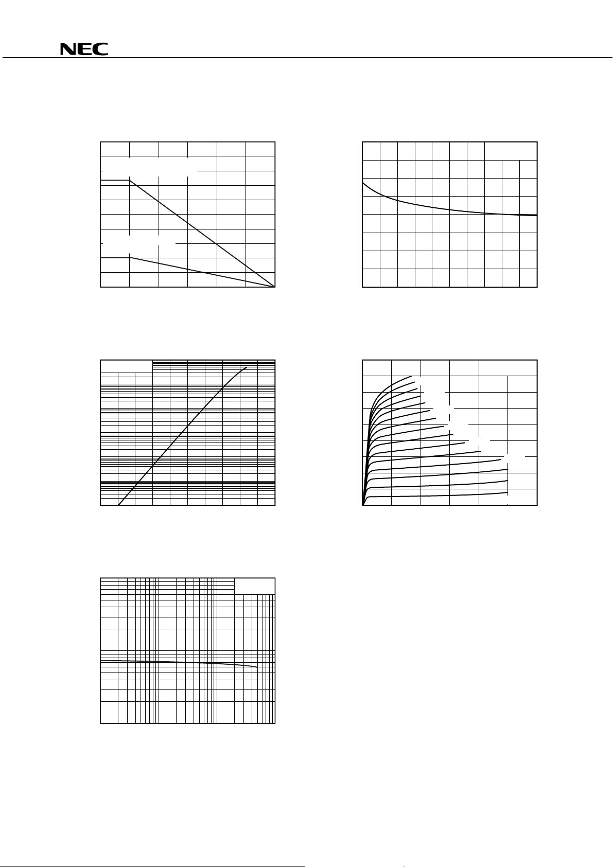
TYPICAL CHARACTERISTICS (Unless otherwise specified, TA = +25°°°°C)
2SC5754
TOTAL POWER DISSIPATION
vs. AMBIENT TEMPERATURE
1 000
Mounted on Polyimide PCB
800
(mW)
(38 × 38 mm, t = 0.4 mm)
tot
735
600
400
Stand alone device
in free air
205
200
Total Power Dissipation P
0 25 50 75 100 125 150
Ambient Temperature TA (˚C)
COLLECTOR CURRENT vs.
BASE TO EMITTER VOLTAGE
1 000
(mA)
C
Collector Current I
0.001
VCE = 3 V
100
10
1
0.1
0.01
0.70.60.5 0.8 0.9 1.0
Base to Emitter Voltage VBE (V)
REVERSE TRANSFER CAPACITANCE
vs. COLLECTOR TO BASE VOLTAGE
2.0
(pF)
re
1.5
1.0
0.5
Reverse Transfer Capacitance C
01 3425
Collector to Base Voltage VCB (V)
f = 1 MHz
COLLECTOR CURRENT vs.
COLLECTOR TO EMITTER VOLTAGE
450
400
350
(mA)
C
300
250
200
150
100
Collector Current I
50
0214536
Collector to Emitter Voltage VCE (V)
7 mA
6 mA
5 mA
4 mA
B
: 0.5 mA step
I
3 mA
IB = 0.5 mA
2 mA
1 mA
1 000
FE
100
DC Current Gain h
10
4
DC CURRENT GAIN vs.
COLLECTOR CURRENT
VCE = 3 V
101 100 1 000
Collector Current IC (mA)
Data Sheet PU10008EJ02V0DS
Page 5
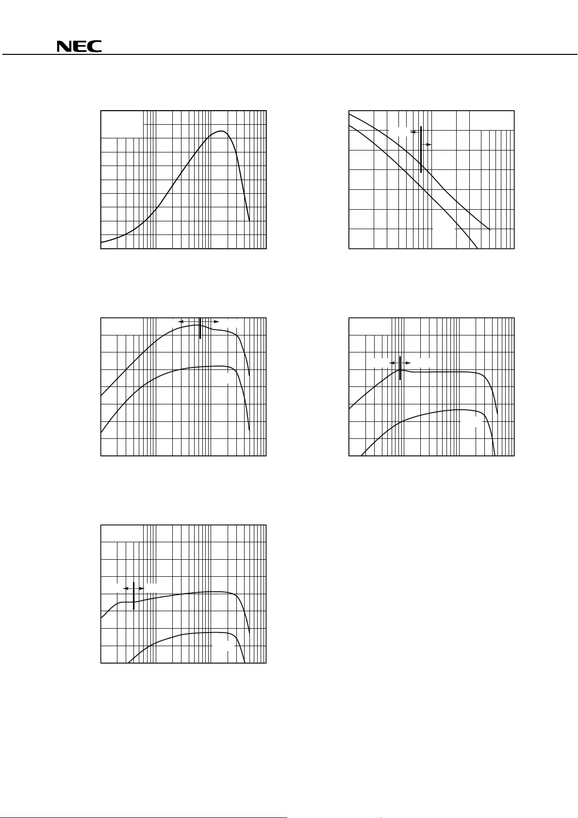
2SC5754
GAIN BANDWIDTH PRODUCT
vs. COLLECTOR CURRENT
25
VCE = 3 V
f = 0.5 GHz
20
(GHz)
T
15
10
5
Gain Bandwidth Product f
0
INSERTION POWER GAIN, MAG, MSG
vs. COLLECTOR CURRENT
20
CE
= 3 V
V
f = 1 GHz
15
(dB)
2
|
21e
10
10 1001 1 000
Collector Current IC (mA)
MAGMSG
2
|S
21e
|
INSERTION POWER GAIN,
MAG, MSG vs. FREQUENCY
35
(dB)
2
|
21e
30
25
20
MSG
MAG
15
10
5
0
Maximum Available Power Gain MAG (dB)
Maximum Stable Power Gain MSG (dB)
Insertion Power Gain |S
0.1 1 10
|S
Frequency f (GHz)
INSERTION POWER GAIN, MAG, MSG
vs. COLLECTOR CURRENT
20
VCE = 3 V
f = 2 GHz
15
(dB)
2
|
21e
10
MAGMSG
21e
2
|
VCE = 3 V
C
= 100 mA
I
5
Insertion Power Gain |S
1 10 100 1 000
0
Maximum Available Power Gain MAG (dB)
Maximum Stable Power Gain MSG (dB)
Collector Current I
INSERTION POWER GAIN, MAG, MSG
vs. COLLECTOR CURRENT
20
VCE = 3 V
f = 2.5 GHz
15
(dB)
2
|
21e
10
5
0
Maximum Available Power Gain MAG (dB)
Maximum Stable Power Gain MSG (dB)
Insertion Power Gain |S
1 10 100 1 000
MAGMSG
Collector Current I
C
(mA)
C
(mA)
2
|S
21e
C
(mA)
|
5
Insertion Power Gain |S
1 10 100 1 000
0
Maximum Available Power Gain MAG (dB)
Maximum Stable Power Gain MSG (dB)
Collector Current I
2
|S
21e
|
Data Sheet PU10008EJ02V0DS
5
Page 6
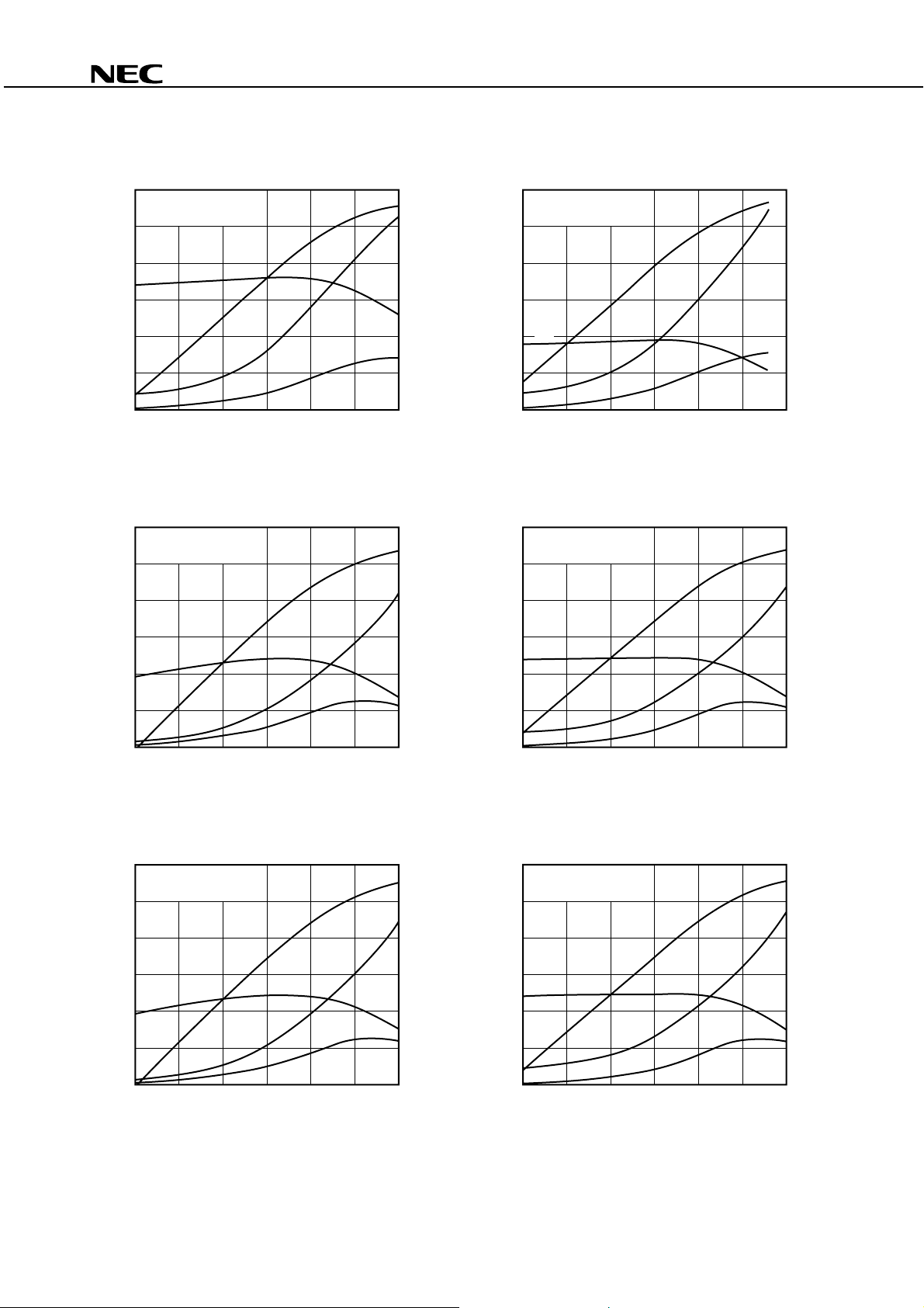
2SC5754
OUTPUT POWER, POWER GAIN,
COLLECTOR CURRENT, COLLECTOR
EFFICIENCY vs. INPUT POWER
30
(dB)
P
VCE = 3.2 V, f = 0.9 GHz
Cq
= 20 mA, 1/2 Duty
I
25
20
G
P
P
out
15
(dBm), Power Gain G
out
10
5
C
0
–15 0–5–10 5 10 15
Output Power P
Input Power P
η
in
(dBm)
OUTPUT POWER, POWER GAIN,
COLLECTOR CURRENT, COLLECTOR
EFFICIENCY vs. INPUT POWER
30
(dB)
P
VCE = 3.2 V, f = 1.8 GHz
Cq
= 4 mA, 1/2 Duty
I
25
P
out
20
15
G
(dBm), Power Gain G
out
10
P
OUTPUT POWER, POWER GAIN,
COLLECTOR CURRENT, COLLECTOR
(%)
C
η
300
250
I
C
200
150
(mA), Collector Efficiency
100
C
50
0
Collector Current I
EFFICIENCY vs. INPUT POWER
30
(dB)
P
VCE = 3.2 V, f = 2.4 GHz
Cq
= 20 mA, 1/2 Duty
I
25
20
15
(dBm), Power Gain G
out
10
G
P
5
0
–5 1050152025
Output Power P
Input Power P
P
out
η
in
(dBm)
I
C
C
(%)
C
η
300
250
200
150
(mA), Collector Efficiency
100
C
50
0
Collector Current I
OUTPUT POWER, POWER GAIN,
COLLECTOR CURRENT, COLLECTOR
(%)
C
η
300
250
200
I
C
150
(mA), Collector Efficiency
100
C
EFFICIENCY vs. INPUT POWER
30
(dB)
P
VCE = 3.2 V, f = 1.8 GHz
Cq
= 20 mA, 1/2 Duty
I
25
P
out
20
15
G
(dBm), Power Gain G
out
P
10
(%)
C
η
300
250
200
I
C
150
(mA), Collector Efficiency
100
C
5
C
η
0
–10 50–5 10 15 20
Output Power P
in
Input Power P
(dBm)
OUTPUT POWER, POWER GAIN,
COLLECTOR CURRENT, COLLECTOR
EFFICIENCY vs. INPUT POWER
30
(dB)
P
VCE = 3.6 V, f = 1.8 GHz
Cq
= 4 mA, 1/2 Duty
I
25
P
out
20
15
G
(dBm), Power Gain G
out
Output Power P
Remark
P
10
5
C
0
–10 50–5 10 15 20
Input Power P
η
in
(dBm)
The graphs indicate nominal characteristics.
50
0
Collector Current I
5
C
0
–10 50–5 10 15 20
Output Power P
Input Power P
η
in
(dBm)
50
0
Collector Current I
OUTPUT POWER, POWER GAIN,
COLLECTOR CURRENT, COLLECTOR
(%)
C
η
300
250
200
I
C
150
(mA), Collector Efficiency
100
C
50
0
Collector Current I
EFFICIENCY vs. INPUT POWER
30
(dB)
P
VCE = 3.6 V, f = 1.8 GHz
Cq
= 20 mA, 1/2 Duty
I
25
P
out
20
15
G
(dBm), Power Gain G
out
Output Power P
P
10
5
C
0
–10 50–5 10 15 20
Input Power P
η
in
(dBm)
(%)
C
η
300
250
200
I
C
150
(mA), Collector Efficiency
100
C
50
0
Collector Current I
6
Data Sheet PU10008EJ02V0DS
Page 7
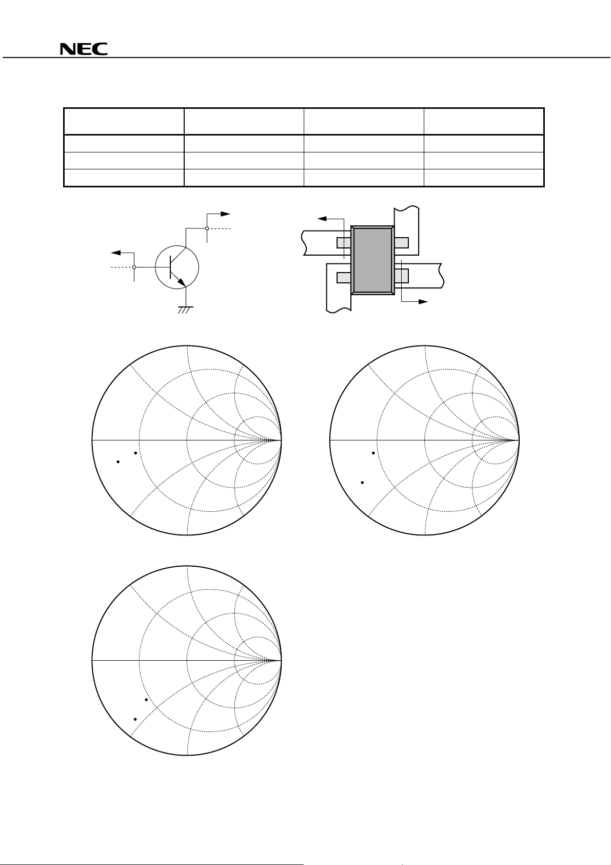
POWER SUPPLY IMPEDANCE, LOAD IMPEDANCE (Recommended value)
2SC5754
Frequency
f (GHz)
Collector to Emitter Voltage
CE
V
(V)
Supply Impedance
ZS (Ω)
0.9 2.8 to 3.6 8.4 − 5.2 j 15.1 − 4.3 j
1.8 2.8 to 3.6 6.3 − 16.4 j 15.8 − 6.9 j
2.4 2.8 to 3.6 5.9 − 22.1 j 15.2 − 17.9 j
Z
L
Z
S
RF input line
GND
Z
S
BEE
GND
C
Tr.
Z
L
f = 0.9 GHz
f = 1.8 GHz
Load Impedance
ZL (Ω)
RF output line
Z
L
Z
S
f = 2.4 GHz
Z
Z
S
Z
L
Z
S
L
Data Sheet PU10008EJ02V0DS
7
Page 8
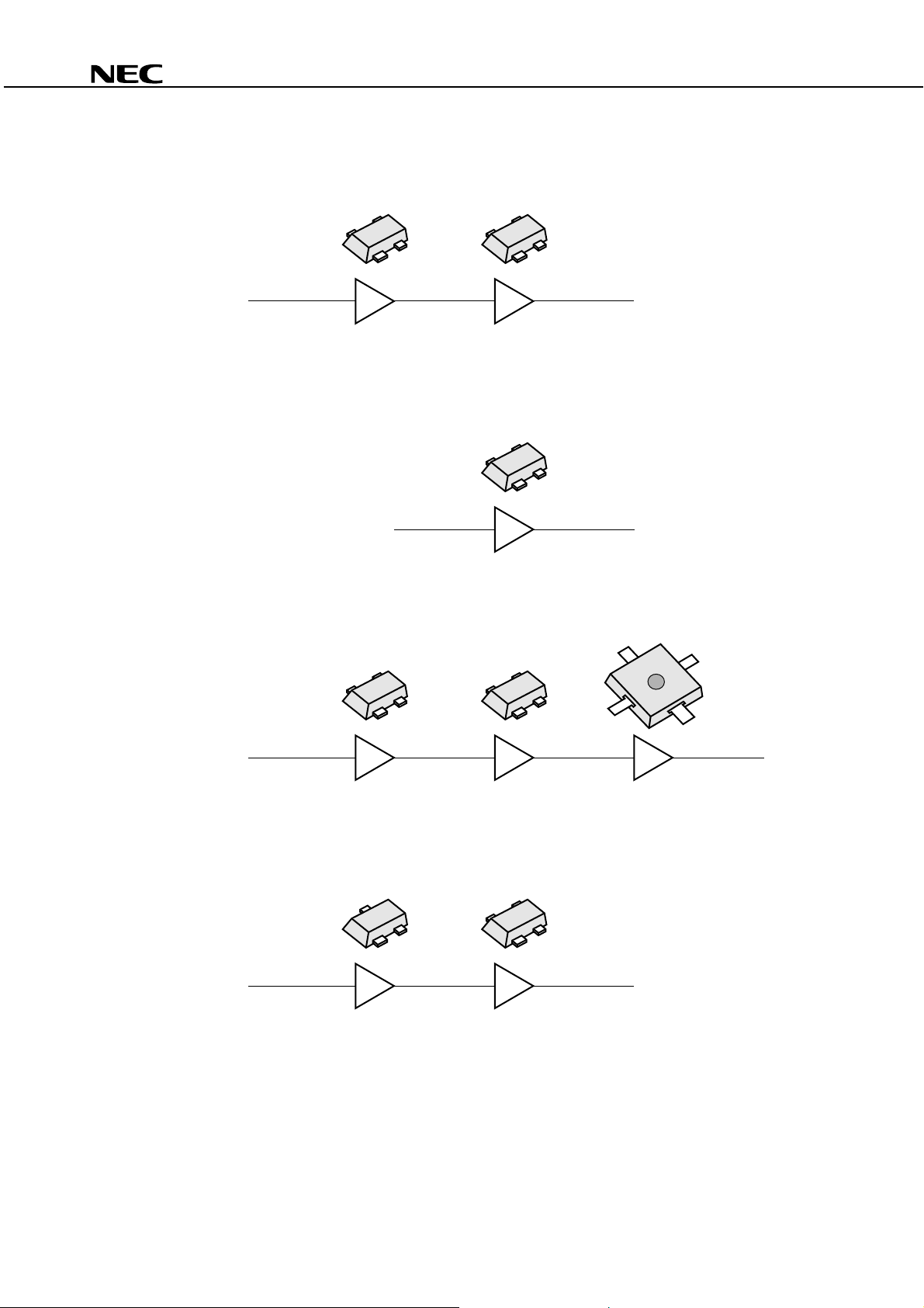
APPLICATION EXAMPLE (Low-cost PA solution)
Bluetooth Power Class 1
f = 2.4 GHz
2SC5754
T80
0 dBm 13 dBm 22 dBm
2SC5509 2SC5754
SS Cordless Phone
f = 2.4 GHz
DCS1800 (GSM1800) Cellular Phone
f = 1.8 GHz
R55
R57
R57
20 dBm 26 dBm
2SC5754
R57
A 3
9Z001
Cordless Phone
f = 0.9 GHz
5 dBm 16 dBm 25 dBm 35 dBm
2SC5753 2SC5754 NE5520379A
T H
–3 dBm 9 dBm 25 dBm
2SC5434
(3-pin TUSMM)
R57
2SC5754
(MOS FET)
8
Data Sheet PU10008EJ02V0DS
Page 9
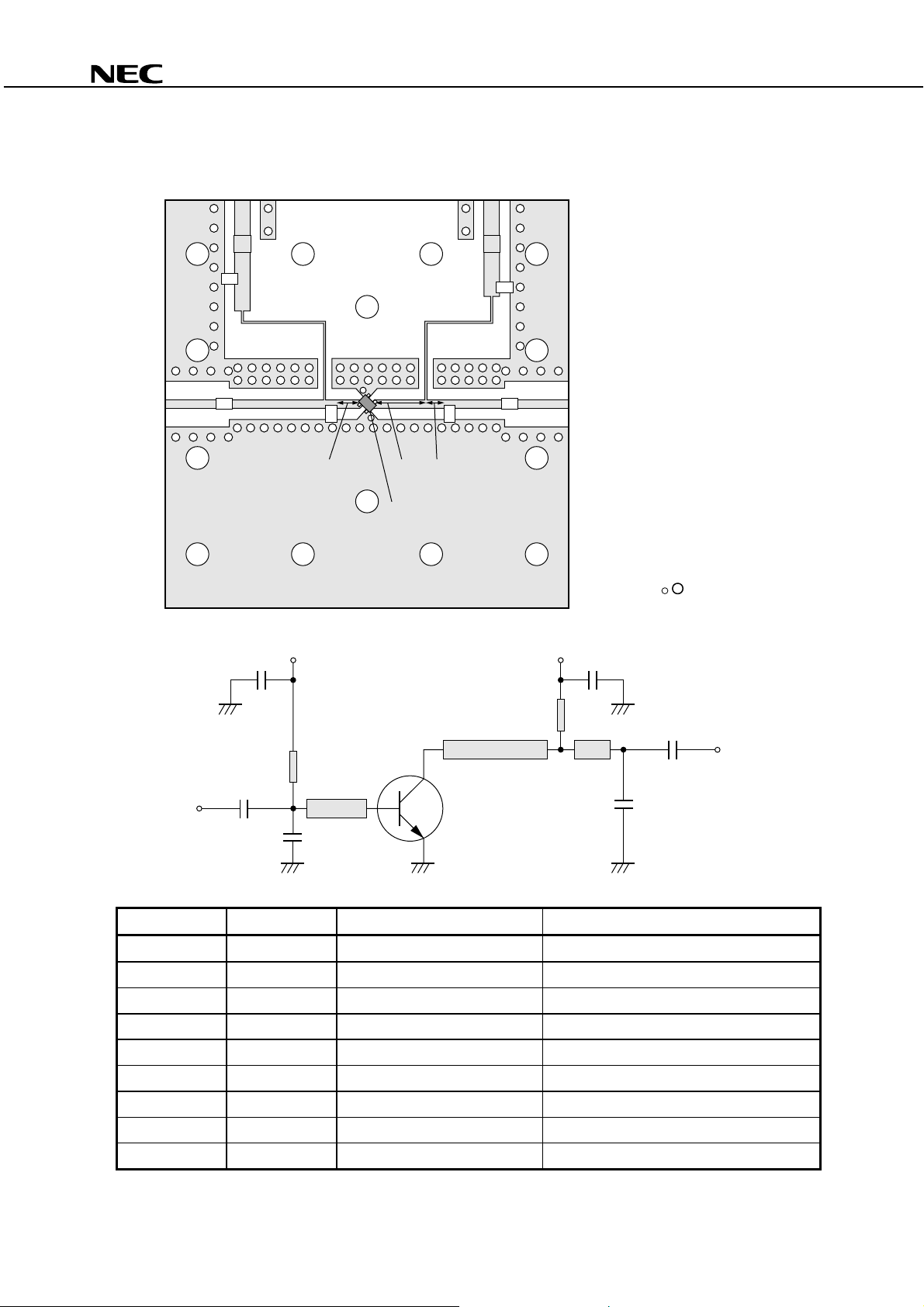
EVALUATION CIRCUIT EXAMPLE : 1.8 GHz PA EVALUATION BOARD
PCB Pattern and Element Layout
B
V
V
C
2SC5754
C2
SL1 SL4
RF in RF out
C1
SL2
C3
SL3 SL5
Tr. (2SC5754)
C4
C6
C5
Equivalent Circuit
V
RF in
C1
B
SL3
SL1
SL2
Tr.
V
C
Remarks 1. 38 × 38 mm, t = 0.4 mm,
r
ε
= 4.55 double-sided
copper-clad polyimide board
2. Back side : GND pattern
3. Solder plating on pattern
4. : Through holes
C4C2
SL4
SL5 C6
RF out
C5
C3
Parts List
Parts Value Size Classification
C1, C6 18 pF Multiplayer ceramic chip capacitor
C2 3 300 pF Multiplayer ceramic chip capacitor
C3 3 pF Multiplayer ceramic chip capacitor
C4 15 pF Multiplay er ceramic chip capacitor
C5 1.5 pF Multiplayer ceramic chip capacitor
SL1, SL4 w = 0.20 mm Strip line
SL2 w = 0.76 mm, l = 2.5 mm Strip line
SL3 w = 0.76 mm, l = 5 mm Strip line
SL5 w = 0.76 mm, l = 1.5 mm Strip line
Data Sheet PU10008EJ02V0DS
9
Page 10
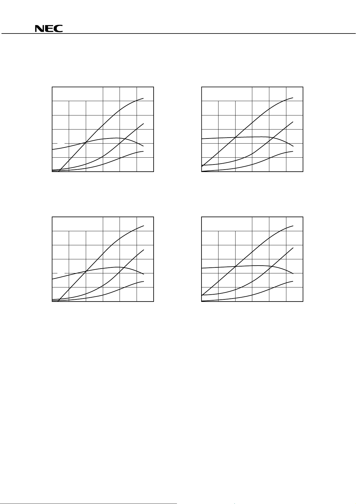
EXAMPLE OF CHARACTERISTICS FOR 1.8 GHz PA EVALUATION BOARD
2SC5754
OUTPUT POWER, POWER GAIN,
COLLECTOR CURRENT, COLLECTOR
EFFICIENCY vs. INPUT POWER
30
(dB)
P
VCE = 3.2 V, f = 1.8 GHz
I
Cq
= 4 mA, 1/2 Duty
25
P
20
out
15
(dBm), Power Gain G
out
10
G
P
5
C
η
0
–10 50–5 10 15 20
Output Power P
Input Power P
in
(dBm)
OUTPUT POWER, POWER GAIN,
COLLECTOR CURRENT, COLLECTOR
EFFICIENCY vs. INPUT POWER
30
(dB)
P
VCE = 3.6 V, f = 1.8 GHz
Cq
= 4 mA, 1/2 Duty
I
25
P
20
15
(dBm), Power Gain G
out
10
G
P
out
OUTPUT POWER, POWER GAIN,
COLLECTOR CURRENT, COLLECTOR
(%)
C
η
300
250
200
I
C
150
(mA), Collector Efficiency
100
C
50
0
Collector Current I
EFFICIENCY vs. INPUT POWER
30
(dB)
P
VCE = 3.2 V, f = 1.8 GHz
I
Cq
= 20 mA, 1/2 Duty
25
P
20
15
G
(dBm), Power Gain G
out
P
10
5
0
–10 50–5 10 15 20
Output Power P
Input Power P
out
η
in
(dBm)
C
(%)
C
η
300
250
200
I
C
150
(mA), Collector Efficiency
100
C
50
0
Collector Current I
OUTPUT POWER, POWER GAIN,
COLLECTOR CURRENT, COLLECTOR
(%)
C
η
300
250
200
I
C
150
(mA), Collector Efficiency
100
C
EFFICIENCY vs. INPUT POWER
30
(dB)
P
VCE = 3.6 V, f = 1.8 GHz
Cq
= 20 mA, 1/2 Duty
I
25
P
out
20
15
G
(dBm), Power Gain G
out
P
10
(%)
C
η
300
250
200
I
C
150
(mA), Collector Efficiency
100
C
5
C
0
–10 50–5 10 15 20
Output Power P
Input Power P
Remark
The graphs indicate nominal characteristics.
η
in
(dBm)
50
0
Collector Current I
5
C
0
–10 50–5 10 15 20
Output Power P
Input Power P
η
in
(dBm)
S-PARAMETERS
S-parameters/Noise parameters are provided on the NEC Compound Semiconductor Devices Web site in a form
(S2P) that enables direct import to a microwave circuit simulator without keyboard input.
Click here to download S-parameters.
[RF and Microwave] → [Device Parameters]
URL http://www.csd-nec.com/
50
0
Collector Current I
10
Data Sheet PU10008EJ02V0DS
Page 11
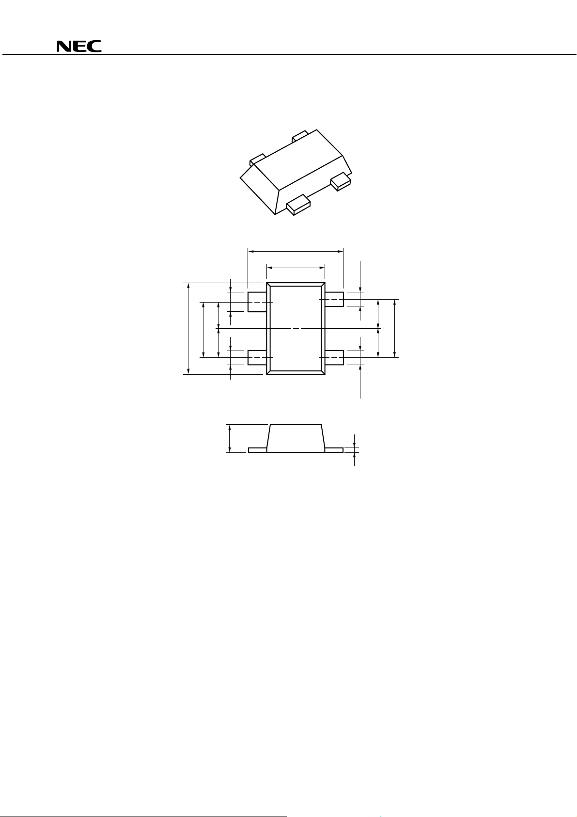
PACKAGE DIMENSIONS
FLAT-LEAD 4-PIN THIN-TYPE SUPER MINIMOLD (M04) (UNIT: mm)
2.05 ± 0.1
–0.05
+0.1
0.40
1.25 ± 0.1
+0.1
0.30
–0.05
R57
0.600.65
1.25
2.0 ± 0.1
2SC5754
0.650.65
1.30
12
–0.05
+0.1
0.30
0.59 ± 0.05
PIN CONNECTIONS
1. Emitter
2. Collector
3. Emitter
4. Base
43
–0.05
+0.1
0.30
–0.05
+0.1
0.11
Data Sheet PU10008EJ02V0DS
11
Page 12
2SC5754
•
The information in this document is current as of March, 2003. The information is subject to change
without notice. For actual design-in, refer to the latest publications of NEC's data sheets or data
books, etc., for the most up-to-date specifications of NEC semiconductor products. Not all products
and/or types are available in every country. Please check with an NEC sales representative for
availability and additional information.
•
No part of this document may be copied or reproduced in any form or by any means without prior
written consent of NEC. NEC assumes no responsibility for any errors that may appear in this document.
•
NEC does not assume any liability for infringement of patents, copyrights or other intellectual property rights of
third parties by or arising from the use of NEC semiconductor products listed in this document or any other
liability arising from the use of such products. No license, express, implied or otherwise, is granted under any
patents, copyrights or other intellectual property rights of NEC or others.
•
Descriptions of circuits, software and other related information in this document are provided for illustrative
purposes in semiconductor product operation and application examples. The incorporation of these
circuits, software and information in the design of customer's equipment shall be done under the full
responsibility of customer. NEC assumes no responsibility for any losses incurred by customers or third
parties arising from the use of these circuits, software and information.
•
While NEC endeavours to enhance the quality, reliability and safety of NEC semiconductor products, customers
agree and acknowledge that the possibility of defects thereof cannot be eliminated entirely. To minimize
risks of damage to property or injury (including death) to persons arising from defects in NEC
semiconductor products, customers must incorporate sufficient safety measures in their design, such as
redundancy, fire-containment, and anti-failure features.
•
NEC semiconductor products are classified into the following three quality grades:
"Standard", "Special" and "Specific". The "Specific" quality grade applies only to semiconductor products
developed based on a customer-designated "quality assurance program" for a specific application. The
recommended applications of a semiconductor product depend on its quality grade, as indicated below.
Customers must check the quality grade of each semiconductor product before using it in a particular
application.
"Standard": Computers, office equipment, communications equipment, test and measurement equipment, audio
and visual equipment, home electronic appliances, machine tools, personal electronic equipment
and industrial robots
"Special": Transportation equipment (automobiles, trains, ships, etc.), traffic control systems, anti-disaster
systems, anti-crime systems, safety equipment and medical equipment (not specifically designed
for life support)
"Specific": Aircraft, aerospace equipment, submersible repeaters, nuclear reactor control systems, life
support systems and medical equipment for life support, etc.
The quality grade of NEC semiconductor products is "Standard" unless otherwise expressly specified in NEC's
data sheets or data books, etc. If customers wish to use NEC semiconductor products in applications not
intended by NEC, they must contact an NEC sales representative in advance to determine NEC's willingness
to support a given application.
(Note)
(1) "NEC" as used in this statement means NEC Corporation, NEC Compound Semiconductor Devices, Ltd.
and also includes its majority-owned subsidiaries.
(2) "NEC semiconductor products" means any semiconductor product developed or manufactured by or for
NEC (as defined above).
M8E 00. 4 - 0110
12
Data Sheet PU10008EJ02V0DS
Page 13

2SC5754
For further information, please contact
NEC Compound Semiconductor Devices, Ltd.
5th Sales Group, Sales Division TEL: +81-44-435-1588 FAX: +81-44-435-1579 E-mail: [email protected]
NEC Compound Semiconductor Devices Hong Kong Limited
Hong Kong Head Office
Taipei Branch Office
Korea Branch Office
NEC Electronics (Europe) GmbH http://www.ee.nec.de/
TEL: +49-211-6503-01 FAX: +49-211-6503-487
California Eastern Laboratories, Inc. http://www.cel.com/
TEL: +1-408-988-3500 FAX: +1-408-988-0279
TEL: +852-3107-7303
TEL: +886-2-8712-0478
TEL: +82-2-558-2120
FAX: +852-3107-7309 E-mail: [email protected]
FAX: +886-2-2545-3859
FAX: +82-2-558-5209
0302-1
 Loading...