NEC 2SC4536 Datasheet

DATA SHEET
DATA SHEET
SILICON TRANSISTOR
MICROWAVE LOW NOISE AMPLIFIER
NPN SILICON EPITAXIAL
TRANSISTOR
2SC4536
DESCRIPTION
The 2SC4536 is designed for use in middle power, low distortion low
noise figure RF amplifier. It features excellent linearity and large dynamic
range, which make it suitable for CATV, telecommunication, and other use,
it employs plastic surface mount type package (SOT-89).
FEATURES
• Low Distortion
IM2 = 57.5 dB TYP. @ VCE = 10 V, IC = 50 mA
IM3 = 82 dB TYP. @ VCE = 10 V, IC = 50 mA
• Low Noise
NF = 1.5 dB TYP. @ VCE = 10 V, IC = 10 mA, f = 1 GHz
• Power Mini Mold Package Used. High Power Dissipation.
ABSOLUTE MAXIMUM RATINGS (TA = 25
Maximum Voltage and Current (TA = 25 C)
Collector to Base Voltage V
Collector to Emitter Voltage V
Emitter to Base Voltage V
Collector Current I
Maximum Power Dissipation
Total Power Dissipation
at 25 C Ambient Temperature PT* 2.0 W
Maximum Temperatures
Junction Temperature T
Storage Temperature Range T
2
* 0.7 mm 16 cm
double sided ceramic substrate. (Copper plating)
CBO
CEO
EBO
C
j
stg
C)
30 V
15 V
3.0 V
250 mA
150
65 to +150C
C
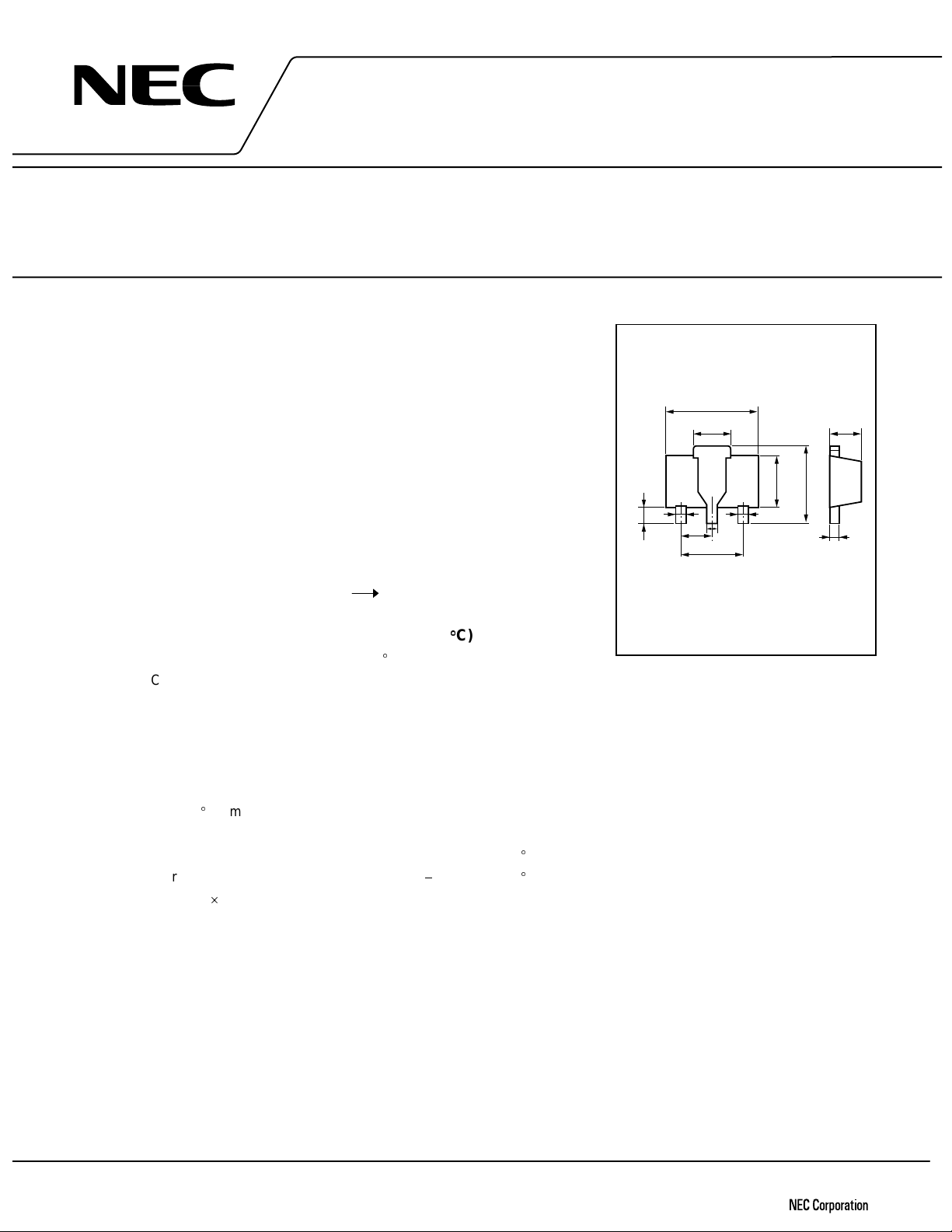
PACKAGE DIMENSIONS
0.42
±0.06
0.8 MIN.
(Unit: mm)
4.5±0.1
1.6±0.2
C
EB
1.5
0.47
±0.06
3.0
Term, Connection
E
: Emitter
C
: Collector (Fin)
B
: Base
(SOT-89)
2.5±0.1
0.42±0.06
1.5±0.1
4.0±0.25
0.41
−0.03
+0.05
Document No. P10369EJ2V1DS00 (2nd edition)
Date Published March 1997 N
Printed in Japan
1994©

2SC4536
ELECTRICAL CHARACTERISTICS (TA = 25
CHARACTERISTIC SYMBOL MIN. TYP. MAX. UNIT TEST CONDITIONS
Collector Cutoff Current I
Emitter Cutoff Current I
DC Current Gain h
Insertion Power Gain
Noise Figure 1 NF
Noise Figure 2 NF
2nd Intermodulation Distortion IM
3rd Intermodulation Distortion IM
Pulsed: PW 350 s, Duty Cycle 2 %
*1
S
R
= RL = 50 , untuned
*2
FE
Classification
h
Class QQ QR QS
Marking QQ QR QS
FE
h
40 to 80 60 to 120 100 to 200
CBO
EBO
FE
21e
S
1
2
2
3
40 200 VCE = 10 V, IC = 50 mA
2
5.5 7.3 dB
C)
5.0
5.0
1.5 dB
2.0 dB
59.0 dB VCE = 10 V, IC = 50 mA, RS = RL = 75
82.0 dB VCE = 10 V, IC = 50 mA, RS = RL = 75
AVCB = 20 V, IE = 0
AVEB = 2 V, IC = 0
CE
V
= 10 V, IC = 50 mA, f = 1 GHz
CE
V
= 10 V, IC = 50 mA, f = 500 MHz
CE
V
= 10 V, IC = 50 mA, f = 1 GHz
Pin = 105 dBV/75 , f
2
= 90 MHz, f = f1 f
f
Pin = 105 dBV/75 , f
2
= 200 MHz, f = 2 f1 f
f
1
2
1
*1
*2
*2
= 190 MHz
= 190 MHz
2
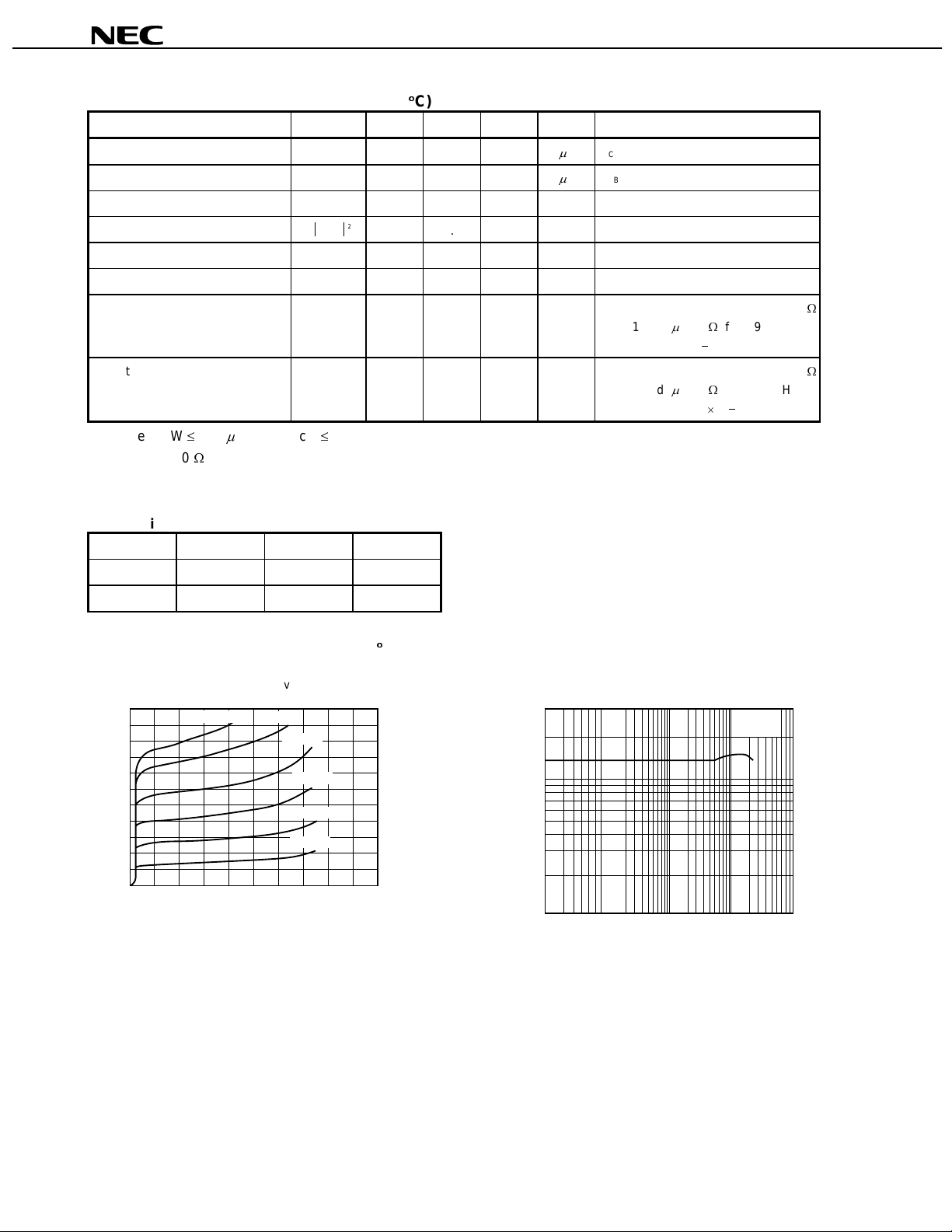
TYPICAL CHARACTERISTICS (TA = 25
COLLECTOR CURRENT vs.
COLLECTOR TO EMITTER VOLT A GE
100
IB = 0.6 mA
80
60
40
-Collector Current-mA
C
20
I
0
V
CE
-Collector to Emitter Voltage-V
0.5 mA
0.4 mA
0.3 mA
0.2 mA
0.1 mA
10
20
C)
DC CURRENT GAIN vs.
COLLECTOR CURRENT
300
100
50
-DC Current Gain
FE
h
10
10 10010.1
I
C
-Collector Current-mA
VCE = 10 V
1000
2

2SC4536
GAIN BANDWIDTH PRODUCT vs.
COLLECTOR CURRENT
10
VCE = 10 V
5
1
0.5
-Gain Bandwidth Product-GHz
T
f
0.2
5 1005010 300
C
-Collector Current-mA
I
INSERTION POWER GAIN, MAXIMUM POWER GAIN AND
MAXIMUM AVAILABLE GAIN vs. COLLECTOR CURRENT
10
VCE = 10 V
f = 1 GHz
8
G
|S
MAG
max(u)
21e
2
|
6
FEED-BACK CAPACIATNCE vs.
COLLECTOR TO BASE VOLTAGE
5.0
f = 1 MHz
I
E
= 0
1.0
0.5
-Feed-Back Capacitance-pF
re
C
0.2
1 5 10 30
CB
-Collector to Base Voltage-V
V
INSERTION POWER GAIN, MAXIMUM POWER GAIN AND
MAXIMUM AVAILABLE GAIN vs. FREQUENCY
VCE = 10 V
IC = 50 mA
G
max(u)
20
2
|S
21e
|
4
-Insertion Power Gain-dB
2
|
-Maximum Power Gain-dB
21e
max
2
|S
G
MAG-Maximum Available Gain-dB
0
10 50 100 300
C
-Collector Current-mA
I
10
-Insertion Power Gain-dB
2
|
-Maximum Power Gain-dB
21e
max
G
MAG-Maximum Available Gain-dB
|S
0
0.1 0.5 1 32
MAG
f-Frequency-GHz
3
