

Page 1
DATA SHEET
SILICON TRANSISTOR
2SC4227
HIGH FREQUENCY LOW NOISE AMPLIFIER
NPN SILICON EPITAXIAL TRANSISTOR
SUPER MINI MOLD
DESCRIPTION
The 2SC4227 is a low supply voltage transistor designed for VHF,
UHF low noise amplifier.
It is suitable for a high density surface mount assembly since the
transistor has been applied small mini mold package.
FEATURES
• Low Noise
NF = 1.4 dB TYP. @ f = 1 GHz, VCE = 3 V, IC = 7 mA
• High Gain
2
21e|
= 12 dB TYP. @ f = 1 GHz, VCE = 3 V, IC = 7 mA
|S
• Small Mini Mold Package
EIAJ: SC-70
ORDERING INFORMATION
PART
NUMBER
2SC4227-T1 3 Kpcs/Reel. Embossed tape 8 mm wide.
2SC4227-T2 3 Kpcs/Reel. Embossed tape 8 mm wide.
QUANTITY PACKING STYLE
Pin3 (Collector) face to perforation side
of the tape.
Pin1 (Emitter), Pin2 (Base) face to
perforation side of the tape.
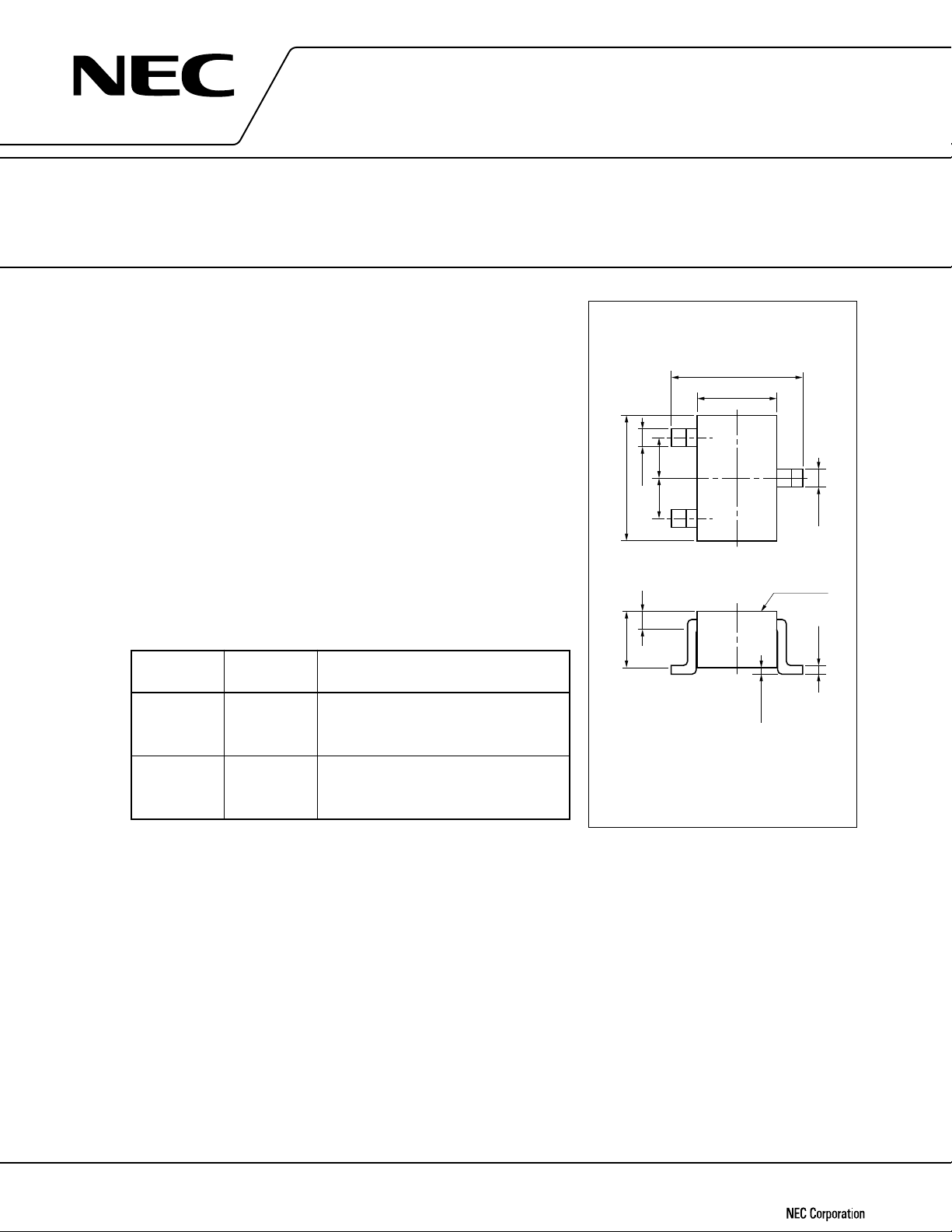
PACKAGE DIMENSIONS
in millimeters
2.1 ± 0.1
1.25 ± 0.1
+0.1
2.0 ± 0.2
0.9 ± 0.1
2
–0
0.3
1
0.65 0.65
0.3
PIN CONNECTIONS
Emitter
1.
Base
2.
Collector
3.
Marking
0 to 0.1
3
–0
+0.1
0.3
–0.05
+0.1
0.15
* Please contact with responsible NEC person, if you require evaluation
sample. Unit sample quantity shall be 50 pcs. (Part No.: 2SC4227)
Document No. P10371EJ2V0DS00 (2nd edition)
(Previous No. TC-2403)
Date Published July 1995 P
Printed in Japan
©
1993
Page 2
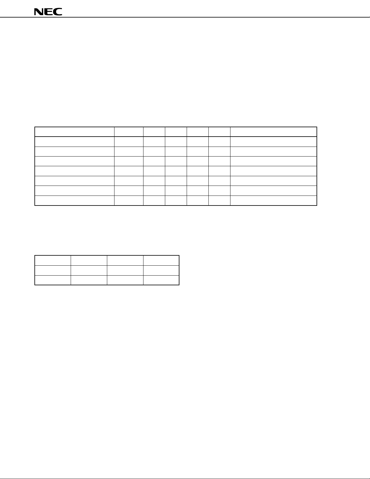
ABSOLUTE MAXIMUM RATINGS (TA = 25 ˚C)
Collector to Base Voltage VCBO 20 V
Collector to Emitter Voltage V
CEO 10 V
Emitter to Base Voltage VEBO 1.5 V
Collector Current IC 65 mA
Total Power Dissipation P
T 150 mW
Junction Temperature Tj 150 °C
Storage Temperature Tstg –65 to +150 °C
ELECTRICAL CHARACTERISTICS (TA = 25 ˚C)
CHARACTERISTIC SYMBOL MIN. TYP. MAX. UNIT TEST CONDITION
Collector Cutoff Current ICBO 0.8
Emitter Cutoff Current IEBO 0.8
DC Current Gain hFE 40 240 VCE = 3 V, IC = 7 mA
Gain Bandwidth Product fT 4.5 7.0 GHz VCE = 3 V, IC = 7 mA
Feedback Capacitance Cre 0.45 0.9 pF VCE = 3 V, IE = 0, f = 1 MHz
Insertion Power Gain |S21e|
Noise Figure NF 1.4 2.7 dB VCE = 3 V, IC = 7 mA, f = 1 GHz
2
10 12 dB VCE = 3 V, IC = 7 mA, f = 1 GHz
µ
AVCB = 10 V, IE = 0
µ
AVEB = 1 V, IC = 0
*1
2SC4227
*2
*1 Pulse Measurement ; PW ≤ 350 µs, Duty Cycle ≤ 2 % Pulsed.
*2 Measured with 3 terminals bridge, Emitter and Case should be grounded.
FE Classification
h
Rank R33 R34 R35
Marking R33 R34 R35
hFE 40 to 90 70 to 150 110 to 240
2
Page 3
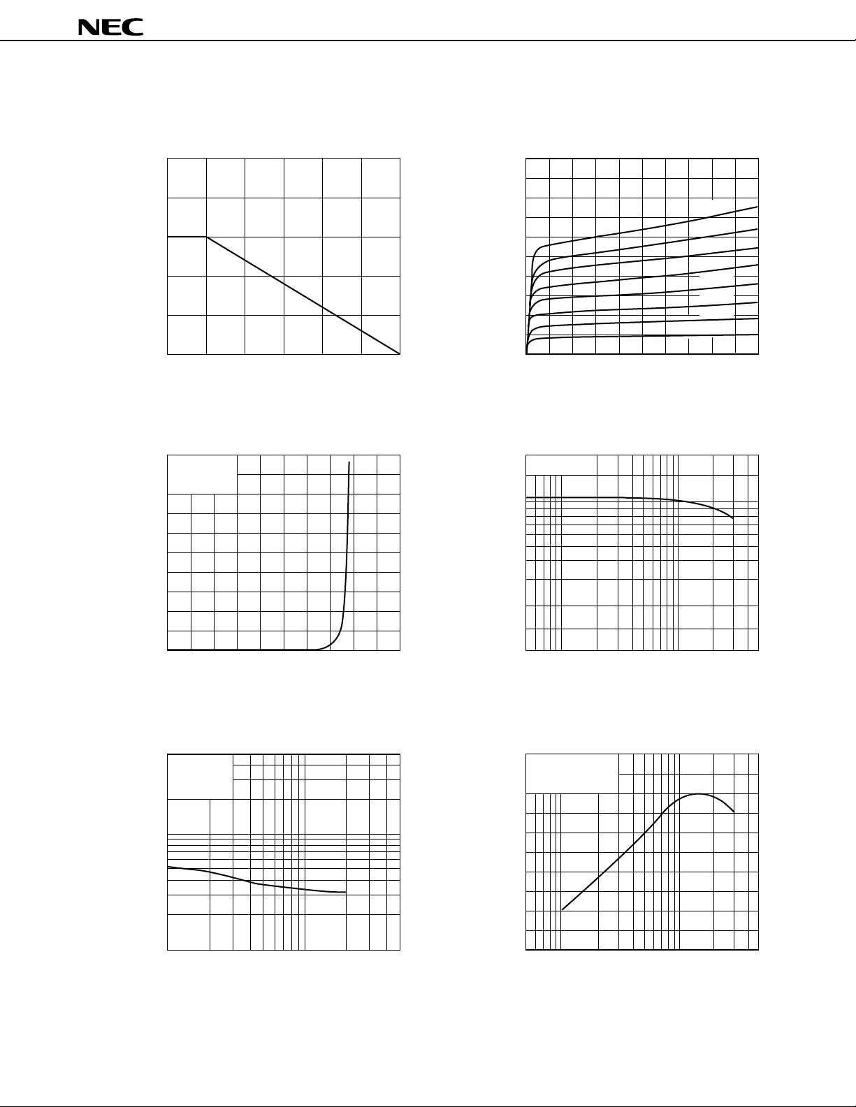
TYPICAL CHARACTERISTICS (TA = 25 ˚C)
2SC4227
TOTAL POWER DISSIPATION vs.
AMBIENT TEMPERATURE
200
100
– Total Power Dissipation – mW
T
P
0
50 100 150
TA – Ambient Temperature – °C VCE – Collector to Emitter Voltage – V
COLLECTOR CURRENT vs.
BASE TO EMITTER VOLTAGE
20
CE
= 3 V
V
COLLECTOR CURRENT vs.
COLLECTOR TO EMITTER VOLTAGE
25
20
15
10
– Collector Current – mA
5
C
I
0
DC CURRENT GAIN vs.
COLLECTOR CURRENT
200
VCE = 3 V
100
160 A
µ
140 A
µ
120 A
µ
100 A
µ
80 A
µ
60 A
µ
µ
40 A
µ
I
B
= 20 A
0.5 1.0
10
– Collector Current – mA
C
I
0 0.5 1.0
VBE – Base to Emitter Voltage – V
FEED-BACK CAPACITANCE vs.
COLLECTOR TO BASE VOLTAGE
5.0
f = 1 MHz
2.0
1.0
0.5
0.2
– Feed-back Capacitance – pF
re
C
0.1
1
2 5 10 20 50
V
CB
– Collector to Base Voltage – V
50
– DC Current Gain
FE
h
20
10
0.5
1 5 10 50
I
C
– Collector Current – mA
GAIN BANDWIDTH PRODUCT vs.
COLLECTOR CURRENT
10
V
CE
= 3 V
f = 1 GHz
8
6
4
2
– Gain Bandwidth Product – GHz
T
f
0
0.5
1.0 5.0 10 50
IC – Collector Current – mA
3
Page 4
2SC4227
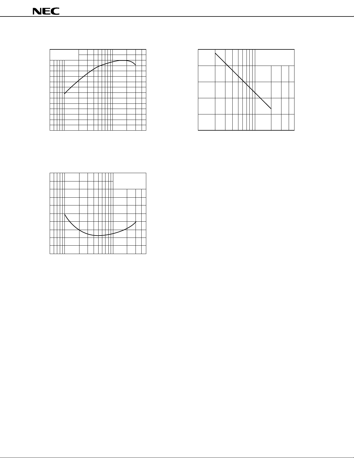
INSERTION POWER GAIN vs.
COLLECTOR CURRENT
15
CE
= 3 V
V
f = 1 GHz
10
5
– Insertion Power Gain – dB
2
|
21e
|S
0
0.5
1 5 10 50
IC – Collector Current – mA
NOISE FIGURE vs.
COLLECTOR CURRENT
5
4
V
CE
= 3 V
f = 1 GHz
INSERTION POWER GAIN vs.
FREQUENCY
25
V
CE
I
C
= 7 mA
20
15
10
– Insertion Power Gain – dB
2
|
5
21e
|S
0
0.1 1.00.5 5.0
0.2 2.0
f – Frequency – GHz
= 3 V
3
2
NF – Noise Figure – dB
1
0
0.5
1.0 5.0 10 50
IC – Collector Current – mA
4
Page 5

S-PARAMETER
(VCE = 3 V, IC = 7 mA, ZO = 50 Ω)
FREQUENCY S11 S21 S12 S22
MHz MAG ANG MAG ANG MAG ANG MAG ANG
100.00 .804 –23.8 11.631 154.8 .023 74.8 .920 –16.5
200.00 .692 –48.6 10.839 137.5 .040 64.1 .791 –27.7
300.00 .581 –70.3 9.722 123.8 .050 59.9 .675 –33.5
400.00 .489 –89.0 8.519 112.9 .060 56.7 .597 –37.0
500.00 .419 –104.9 7.434 104.1 .067 55.9 .538 –38.7
600.00 .376 –117.1 6.468 97.5 .075 55.6 .497 –40.0
700.00 .342 –128.6 5.729 91.8 .082 55.7 .467 –41.0
800.00 .321 –138.4 5.115 86.7 .089 56.3 .443 –41.7
900.00 .305 –147.3 4.630 82.5 .096 56.1 .427 –42.5
1000.00 .296 –155.2 4.207 78.5 .104 56.4 .412 –43.6
1100.00 .289 –162.2 3.879 74.8 .111 56.0 .401 –44.6
1200.00 .284 –169.3 3.595 71.4 .119 56.4 .393 –45.8
1300.00 .282 –175.3 3.349 68.1 .127 56.2 .384 –47.3
1400.00 .281 179.0 3.133 64.8 .136 56.0 .379 –48.8
1500.00 .283 173.8 2.945 61.9 .143 55.4 .372 –50.1
1600.00 .283 168.6 2.780 58.8 .151 55.0 .367 –51.8
1700.00 .285 163.8 2.631 56.2 .160 54.4 .363 –53.7
1800.00 .286 159.9 2.514 53.3 .168 53.9 .359 –55.4
1900.00 .289 155.4 2.390 50.5 .177 53.3 .354 –57.3
2000.00 .293 151.8 2.293 47.8 .186 52.5 .351 –59.2
2SC4227
(V
CE = 3 V, IC = 5 mA, ZO = 50 Ω)
FREQUENCY S11 S21 S12 S22
MHz MAG ANG MAG ANG MAG ANG MAG ANG
100.00 .818 –29.4 14.580 156.2 .023 79.9 .932 –14.4
200.00 .689 –54.3 12.120 137.5 .040 65.1 .824 –23.4
300.00 .594 –73.1 10.142 124.6 .052 55.0 .716 –30.3
400.00 .500 –89.8 8.340 114.4 .063 58.5 .620 –32.2
500.00 .457 –102.8 7.300 107.5 .069 56.4 .577 –34.2
600.00 .404 –115.0 6.211 101.0 .081 54.9 .525 –35.1
700.00 .377 –124.4 5.496 96.8 .084 59.5 .511 –36.1
800.00 .359 –134.3 4.908 91.4 .091 58.4 .471 –36.2
900.00 .342 –141.5 4.450 88.1 .097 58.4 .458 –35.3
1000.00 .335 –150.3 4.018 84.7 .100 61.2 .440 –36.5
1100.00 .326 –155.9 3.750 81.4 .112 61.8 .442 –36.8
1200.00 .321 –162.4 3.410 78.1 .115 61.4 .417 –37.8
1300.00 .317 –167.2 3.181 75.6 .124 62.3 .412 –38.5
1400.00 .321 –173.4 2.995 72.5 .131 63.9 .411 –39.9
1500.00 .318 –177.5 2.802 69.8 .138 63.6 .407 –40.4
1600.00 .320 176.6 2.665 67.3 .149 66.4 .400 –41.1
1700.00 .323 173.2 2.533 66.1 .156 65.3 .394 –43.7
1800.00 .326 167.8 2.369 63.0 .162 65.9 .394 –44.3
1900.00 .331 165.6 2.275 61.0 .177 65.4 .390 –45.5
2000.00 .333 161.4 2.196 59.2 .183 64.5 .384 –47.6
5
Page 6

S-PARAMETER
(VCE = 3 V, IC = 3 mA, ZO = 50 Ω)
FREQUENCY S11 S21 S12 S22
MHz MAG ANG MAG ANG MAG ANG MAG ANG
100.00 .906 –22.7 9.710 161.6 .026 82.5 .962 –10.6
200.00 .810 –43.7 8.541 145.3 .049 63.8 .895 –18.3
300.00 .742 –60.6 7.695 133.4 .062 58.7 .811 –25.8
400.00 .638 –76.6 6.580 122.4 .073 56.0 .732 –27.7
500.00 .587 –89.8 5.934 114.1 .082 53.4 .680 –31.2
600.00 .524 –102.2 5.148 107.1 .091 49.7 .624 –33.5
700.00 .490 –111.4 4.627 102.2 .094 51.8 .603 –34.4
800.00 .460 –121.4 4.181 96.0 .099 51.2 .568 –35.0
900.00 .435 –129.9 3.827 92.6 .101 52.9 .540 –35.7
1000.00 .427 –138.2 3.443 88.1 .107 50.9 .523 –36.7
1100.00 .404 –144.9 3.199 84.2 .115 53.7 .512 –36.8
1200.00 .399 –151.7 2.989 79.8 .113 56.6 .500 –38.6
1300.00 .392 –157.9 2.779 77.4 .121 54.9 .489 –39.2
1400.00 .392 –163.6 2.638 73.5 .126 56.4 .483 –40.4
1500.00 .386 –169.1 2.443 71.3 .135 56.4 .477 –41.8
1600.00 .380 –174.5 2.344 68.0 .137 60.0 .477 –42.4
1700.00 .382 –179.7 2.239 65.3 .143 59.5 .466 –44.4
1800.00 .389 176.1 2.113 63.0 .151 59.4 .461 –44.9
1900.00 .383 172.5 2.025 61.4 .154 62.6 .456 –46.9
2000.00 .387 168.3 1.922 58.2 .163 62.0 .464 –48.3
2SC4227
(V
CE = 3 V, IC = 7 mA, ZO = 50 Ω)
FREQUENCY S11 S21 S12 S22
MHz MAG ANG MAG ANG MAG ANG MAG ANG
100.00 1.009 –14.5 3.544 168.8 .027 78.6 .994 –5.6
200.00 .955 –29.7 3.359 156.3 .055 73.6 .969 –10.1
300.00 .937 –42.6 3.277 147.1 .073 63.4 .947 –15.9
400.00 .864 –56.2 3.034 136.6 .091 57.7 .898 –18.8
500.00 .838 –67.3 2.891 128.6 .107 51.1 .865 –22.1
600.00 .775 –79.3 2.674 120.0 .116 46.6 .824 –25.8
700.00 .745 –88.5 2.485 114.2 .125 45.2 .803 –27.5
800.00 .708 –99.1 2.338 106.8 .127 41.2 .776 –29.7
900.00 .670 –107.9 2.177 101.4 .132 40.2 .740 –31.5
1000.00 .649 –116.8 2.052 96.0 .135 37.2 .723 –33.7
1100.00 .621 –124.0 1.914 90.8 .131 36.6 .719 –34.2
1200.00 .608 –131.8 1.819 86.0 .129 35.4 .700 –36.3
1300.00 .587 –138.5 1.713 82.4 .130 35.2 .691 –37.6
1400.00 .587 –144.5 1.628 77.7 .128 36.1 .681 –39.2
1500.00 .573 –152.6 1.533 73.4 .127 36.0 .662 –40.7
1600.00 .559 –157.1 1.464 70.3 .124 37.5 .660 –42.7
1700.00 .562 –164.2 1.421 67.2 .120 39.1 .658 –44.0
1800.00 .557 –168.9 1.350 64.7 .122 43.3 .658 –46.0
1900.00 .557 –173.9 1.296 61.1 .122 45.2 .641 –47.8
2000.00 .551 –178.6 1.240 58.0 .124 48.5 .643 –50.1
6
Page 7

[MEMO]
2SC4227
7
Page 8
2SC4227
No part of this document may be copied or reproduced in any form or by any means without the prior written
consent of NEC Corporation. NEC Corporation assumes no responsibility for any errors which may appear in this
document.
NEC Corporation does not assume any liability for infringement of patents, copyrights or other intellectual
property rights of third parties by or arising from use of a device described herein or any other liability arising
from use of such device. No license, either express, implied or otherwise, is granted under any patents,
copyrights or other intellectual property rights of NEC Corporation or others.
While NEC Corporation has been making continuous effort to enhance the reliability of its semiconductor devices,
the possibility of defects cannot be eliminated entirely. To minimize risks of damage or injury to persons or
property arising from a defect in an NEC semiconductor device, customer must incorporate sufficient safety
measures in its design, such as redundancy, fire-containment, and anti-failure features.
NEC devices are classified into the following three quality grades:
“Standard“, “Special“, and “Specific“. The Specific quality grade applies only to devices developed based on
a customer designated “quality assurance program“ for a specific application. The recommended applications
of a device depend on its quality grade, as indicated below. Customers must check the quality grade of each
device before using it in a particular application.
Standard: Computers, office equipment, communications equipment, test and measurement equipment,
audio and visual equipment, home electronic appliances, machine tools, personal electronic
equipment and industrial robots
Special: Transportation equipment (automobiles, trains, ships, etc.), traffic control systems, anti-disaster
systems, anti-crime systems, safety equipment and medical equipment (not specifically designed
for life support)
Specific: Aircrafts, aerospace equipment, submersible repeaters, nuclear reactor control systems, life
support systems or medical equipment for life support, etc.
The quality grade of NEC devices in “Standard“ unless otherwise specified in NEC's Data Sheets or Data Books.
If customers intend to use NEC devices for applications other than those specified for Standard quality grade,
they should contact NEC Sales Representative in advance.
Anti-radioactive design is not implemented in this product.
M4 94.11
8
 Loading...