DATA SHEET
NPN SILICON RF TRANSISTOR
2SC4226
NPN EPITAXIAL SILICON RF TRANSISTOR
FOR HIGH-FREQUENCY LOW-NOISE AMPLIFICATION
3-PIN SUPER MINIMOLD
DESCRIPTION
The 2SC4226 is a low supply voltage transistor designed for VHF, UHF low noise amplifier.
It is suitable for a high density surface mount assembly since the transistor has been applied 3-pin super minimold
package.
FEATURES
• Low noise : NF = 1.2 dB TYP. @ VCE = 3 V, IC = 7 mA, f = 1 GHz
• High gain : S
• 3-pin super minimold package
ORDERING INFORMATION
Part Number Quantity Supplying Form
2
21e
= 9 dB TYP. @ VCE = 3 V, IC = 7 mA, f = 1 GHz
2SC4226 50 pcs (Non reel) • 8 mm wide embossed taping
2SC4226-T1 3 kpcs/reel • Pin 3 (Collector) face the perforation side of the tape
Remark To order evaluation samples, contact your nearby sales office.
The unit sample quantity is 50 pcs.
ABSOLUTE MAXIMUM RATINGS (TA = +25°C)
Parameter Symbol Ratings Unit
Collector to Base Voltage VCBO 20 V
Collector to Emitter Voltage VCEO 12 V
Emitter to Base Voltage VEBO 3 V
Collector Current IC 100 mA
Total Power Dissipation Ptot
Junction Temperature Tj 150 °C
Storage Temperature Tstg −65 to +150 °C
Note Free air
Note
150 mW
Caution Observe precautions when handling because these devices are sensitive to electrostatic discharge.
The information in this document is subject to change without notice. Before using this document, please confirm that
this is the latest version.
Not all devices/types available in every country. Please check with local NEC Compound Semiconductor Devices
representative for availability and additional information.
Document No. PU10450EJ01V0DS (1st edition)
(Previous No. P10368EJ3V0DS00)
Date Published December 2003 CP(K)
Printed in Japan
The mark shows major revised points.
NEC Compound Semiconductor Devices 1993, 2003

2SC4226
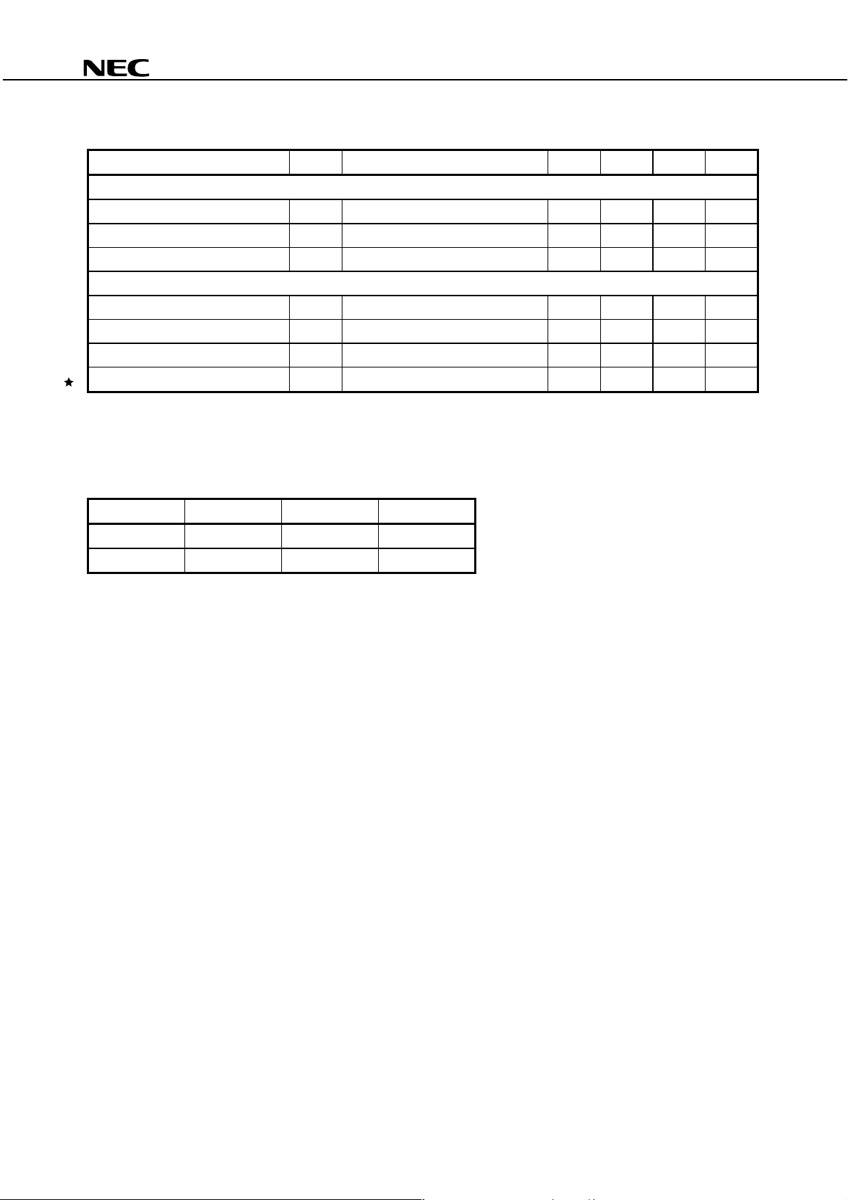
ELECTRICAL CHARACTERISTICS (TA = +25°C)
Parameter Symbol Test Conditions MIN. TYP. MAX. Unit
DC Characteristics
Collector Cut-off Current ICBO VCB = 10 V, IE = 0 mA
Emitter Cut-off Current IEBO VEB = 1 V, IC = 0 mA
DC Current Gain hFE
RF Characteristics
Gain Bandwidth Product fT VCE = 3 V, IC = 7 mA 3.0 4.5 – GHz
Insertion Power Gain S21e2 VCE = 3 V, IC = 7 mA, f = 1 GHz 7 9
Noise Figure NF VCE = 3 V, IC = 7 mA, f = 1 GHz
Reverse Transfer Capacitance Cre
Note 1
VCE = 3 V, IC = 7 mA 40 110 250
Note 2
VCB = 3 V, IE = 0 mA, f = 1 MHz
− −
− −
−
−
1.2 2.5 dB
0.7 1.5 pF
µ
Notes 1. Pulse measurement: PW ≤ 350
s, Duty Cycle ≤ 2%
2. Collector to base capacitance when the emitter grounded
hFE CLASSIFICATION
Rank R23 R24 R25
1.0
1.0
−
µ
µ
−
dB
A
A
Marking R23 R24 R25
hFE Value 40 to 80 70 to 140 125 to 250
2
Data Sheet PU10450EJ01V0DS

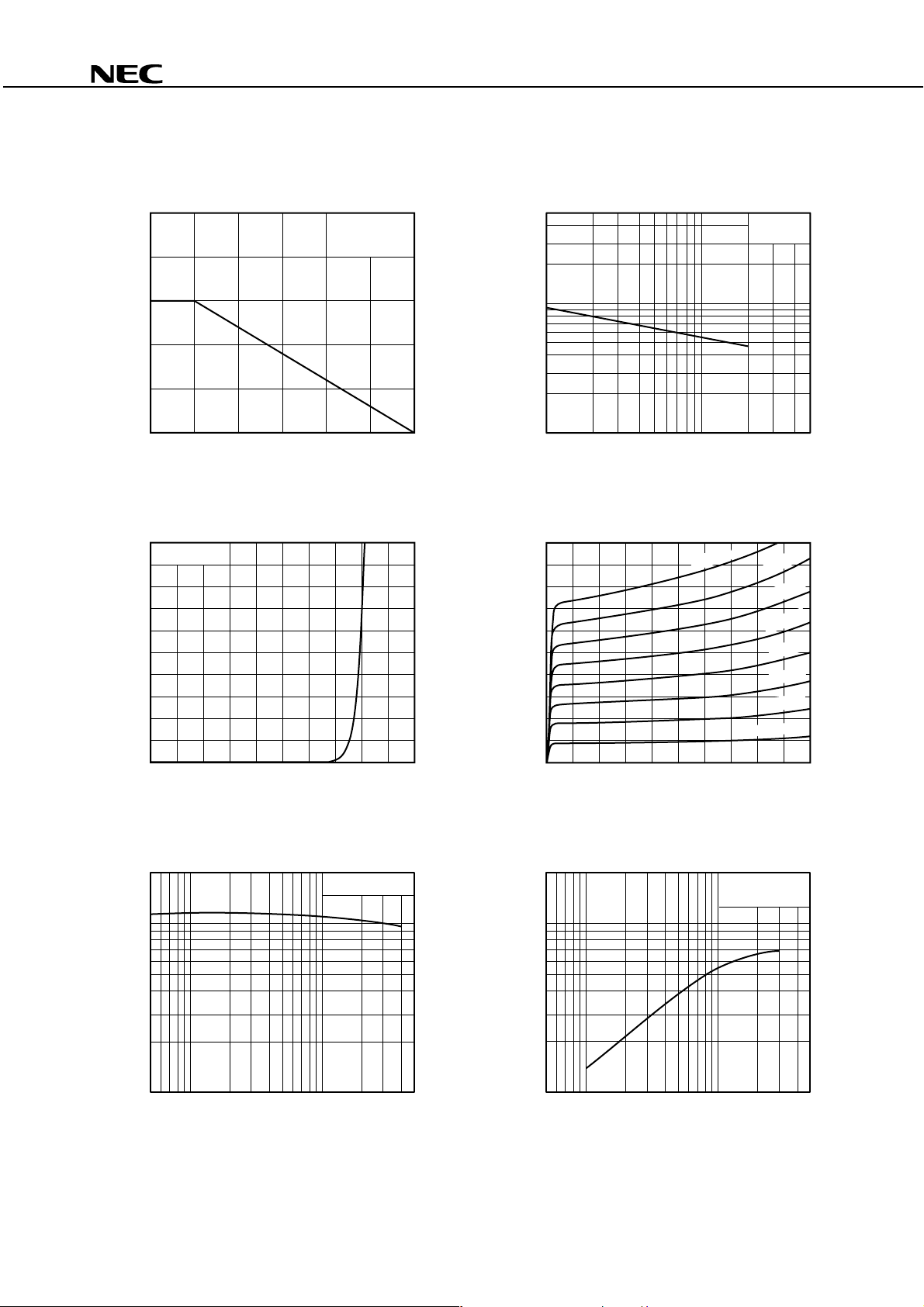
TYPICAL CHARACTERISTICS (TA = +25°C, unless otherwise specified)
250
200
(mW)
tot
TOTAL POWER DISSIPATION
vs. AMBIENT TEMPERATURE
Free Air
REVERSE TRANSFER CAPACITANCE
vs. COLLECTOR TO BASE VOLTAGE
5
(pF)
re
2
2SC4226
f = 1 MHz
150
100
50
Total Power Dissipation P
0
25 50 75 100 125 150
Ambient Temperature TA (˚C)
COLLECTOR CURRENT vs.
BASE TO EMITTER VOLTAGE
20
VCE = 3 V
(mA)
C
10
Collector Current I
1
0.5
0.2
Reverse Transfer Capacitance C
0.1
21 5 10 20 50
Collector to Base Voltage VCB (V)
COLLECTOR CURRENT vs.
COLLECTOR TO EMITTER VOLTAGE
25
20
(mA)
C
15
10
5
Collector Current I
µ
160 A
140 A
120 A
100 A
80 A
60 A
40 A
= 20 A
B
I
µ
µ
µ
µ
µ
µ
µ
0
Base to Emitter Voltage VBE (V)
0.5 1
DC CURRENT GAIN vs.
COLLECTOR CURRENT
200
100
FE
50
DC Current Gain h
20
10
15100.5 50
Collector Current IC (mA)
Remark The graphs indicate nominal characteristics.
VCE = 3 V
Data Sheet PU10450EJ01V0DS
0510
Collector to Emitter Voltage VCE (V)
GAIN BANDWIDTH PRODUCT
vs. COLLECTOR CURRENT
20
(GHz)
10
T
5
2
Gain Bandwidth Product f
1
Collector Current IC (mA)
5100.5 1 50
VCE = 3 V
f = 1 GHz
3
 Loading...