

NEC 2SC3810 Datasheet
DATA SHEET
SILICON TRANSISTOR
2SC3810
NPN SILICON EPITAXIAL TRANSISTOR
FOR MICROWAVE AMPLIFIERS AND ULTRA HIGH SPEED SWITCHINGS
INDUSTRIAL USE
FEATURES
• The 2SC3810 is an NPN silicon epitaxial dual transistor having
a large-gain-bandwidth product performance in a wide operating
current range.
• Dual chips in one package can achieve high performance for
differential amplifiers and current mode logic (CML) circuits.
ABSOLUTE MAXIMUM RATINGS (TA = 25
PARAMETER SYMBOL RATINGS UNIT
Collector to Base Voltage VCBO 20 V
Collector to Emitter Voltage VCEO 10 V
Emitter to Base Voltage VEBO 1.5 V
Collector Current IC 65/unit mA
Total Power Dissipation PT 240/unit mW
Thermal Resistance (junction to case) Rth (j-c) 90/unit °C/W
Junction Temperature Tj 200 °C
Storage Temperature Tstg
°°
°C)
°°
-
65 to +200 °C
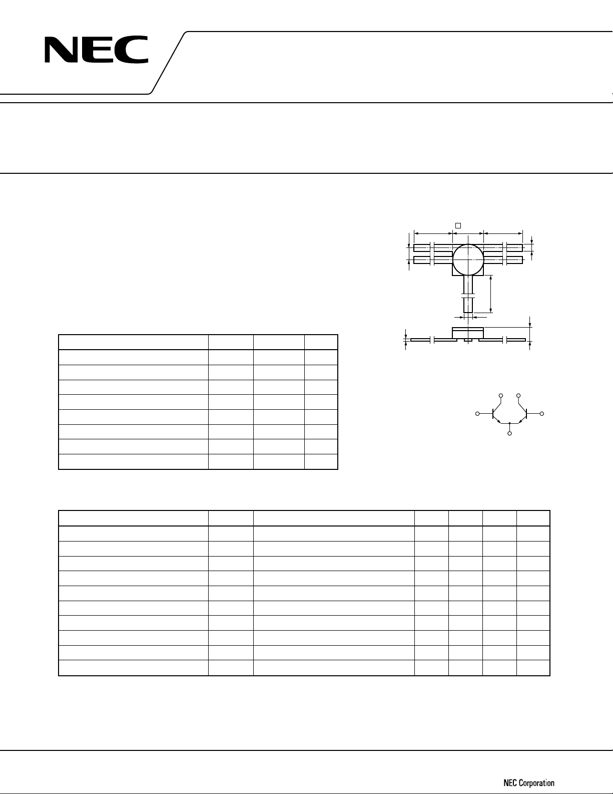
PACKAGE DIMENSIONS (in millimeters)
+0.3
5.0 MIN.
3.5
-
0.2
2
1
5.0 MIN.
0.6 ± 0.1
PIN CONNECTIONS
41
B
1
2
3
1
C
5
E
2
C
1.25 ± 0.1
0.03
+0.06
-
0.1
(#492C)
5.0 MIN.
3
4
5
0.6 ± 0.1
2.0 MAX.
B
2
ELECTRICAL CHARACTERISTICS (TA = 25
PARAMETER SYMBOL TEST CONDITIONS MIN. TYP. MAX. UNIT
Collector to Base Breakdown Voltage BVCBO IC = 10 µA20V
Emitter to Base Breakdown Voltage BVEBO IE = 10 µA, IC = 0 1.5 V
Collector to Emitter Breakdown Voltage
Collector Cut-off Current ICBO VCB = 10 V, IE = 0 1.0
Emitter Cut-off Current IEBO VEB = 1 V, IC = 0 1.0
DC Current Gain hFE VCE = 8 V, IC = 20 mA 50 100 250
hFE Ratio
Difference of Base to Emitter Voltage
Gain Bandwidth Product fT
Feedback Capacitance Cre
Notes 1. hFE1 is the smaller hFE value of the 2 transistors.
2. Measured using a single-type device (equivalent to the 2SC3604).
3. Measured with a 3-terminal bridge, terminals other than the collector and base of the device under test should be connected to
the guard terminal of the bridge.
Document No. P11698EJ1V0DS00 (1st edition)
Date Published July 1996 P
Printed in Japan
BVCEO IC = 1 mA, RBE = ∞ 10 V
Note 1
hFE1/hFE2
∆
VBE VCE = 8 V, IC = 20 mA 30 mV
Note 2
Note 3
°°
°C)
°°
µ
µ
VCE = 8 V, IC = 20 mA 0.6 1.0
VCE = 8 V, IC = 20 mA 7 8 GHz
VCB = 10 V, IE = 0, f = 1.0 MHz 0.5 1.0 pF
©
A
A
1996
2SC3810
REGARDING CLEANSING
Cleanse the flux after soldering. Particularly, cleanse the bottom surface of the transistor so that flux does not remain.
If any flux remains on the bottom surface, it may absorb moisture, resulting in short circuit among pins due to metal-migration
at the metalized area of the transistor. You can use alcohol as a solvent.
Do not apply ultra-sonic-cleaning on this product.
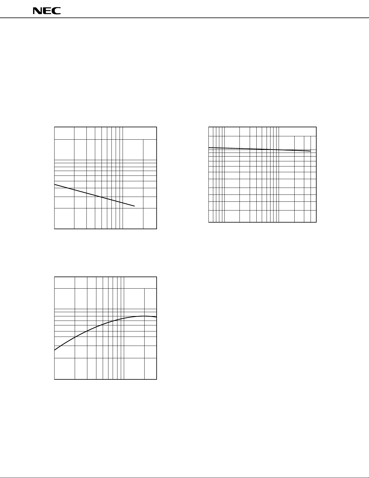
TYPICAL CHARACTERISTICS (TA = 25
FEEDBACK CAPACITANCE vs.
3
2
1
0.7
0.5
0.3
- Feedback Capacitance - pF
re
0.2
C
0.1
30
20
COLLECTOR TO BASE VOLTAGE
1
2 3 5 7 10 20 30
VCB - Collector to Base Voltage - V
GAIN BANDWIDTH PRODUCT vs.
COLLECTOR CURRENT
f = 1.0 MHz
V
CE
= 8 V
°°
°C)
°°
DC CURRENT GAIN vs.
200
100
50
- DC Current Gain
FE
h
20
10
0.5 1 5 10 50
COLLECTOR CURRENT
IC - Collector Current - mA
V
CE
= 8 V
10
7
5
3
2
- Gain Bandwidth Product - GHz
T
f
1
2 3 5 7 10 20 30
I
C
- Collector Current - mA
2
 Loading...