

Page 1

The Core Memory Project
^ ] L T l >>M ' 1¾ :} lU i i V M
www.thecorememory.com
*/•:.-‘' . A ' * * y •
*
•i.jit'.;'. J-.'i'tv'-'.i.-.VJ -. -. 1
-, >, ' *:' • ‘ x'Jlf'$A
?'■? »;■;=,> * S, fc, : : %
1 -' ‘'i h. r / .:,1(:-.¾¾. ■
' ' . ‘V' • ’ *•.*• :'\;■ /■?* / .ift'-iV 1 ~ */ ‘hv
, ;v:„ V yij: <$-{■ K r.y><..
. . ' . ' ' . v ^ r :,‘ *s.’ '\V •
■ ,: . i.-- . j . ' . v , , . : •
• . - «■ :• -. 1 r • -,
‘t './ i *. , . ■. y . ,■; . v./v
- • --: ■
•■■ *• i//
Page 2

The Core Memory Project
Preface
This manual describes the N CR 286 Card (to be referred to as
processor board) and its interfaces. Both the power-fail recovery
(P FR) card and the non-power fail recovery (NPFR) card descriptions
are included in this publication. The Card supports three processing
speeds, 6.0MHz, 8.0MHz, and 10.0MHz, and allows operation at two
speeds. The speed is user selectable and may be set to either 6.0MHz
and 8.0MHz or 6.0MHz and 10.0MHz depending on the processor
board. The default speed is 6.0MHz for both boards. The higher
speed is determined by the frequency of the crystal oscillator. The 6/8
board has a 16.0MHz crystal and the 6/10 board lias a 20.0MIIz crystal.
These boards utilize N CR ’s split board architecture (SB A), in which
major system components are placed on different pluggable cards.
The information in this publication is for reference and is intended for
system integrators and anyone else who needs to understand the
design of the N CR 286 Cards.
www.thecorememory.com
This manual consists of eight chapters:
o The first chapter gives general information about the board
including its physical dimensions, electrical, environmental, and
safety characteristics, and shipping considerations.
o The second chapter gives the functional description of the board's
main components and describes its interfaces, system timing,
address maps, and connectors.
Q Chapter three contains information on switch settings, jumper
strappings, and adjustments.
o Chapter four describes level 0 diagnostics.
/
Page 3

• (,'liaptcr live contains pin-outs for tlie main "tmponenls on the
The Core1 Memory Project
• Chapter six contains board specifications information.
• Chapter seven contains logic diagrams.
• Chapter eight contains the 80286 instruction set.
Contents
286 Card
Technical Reference
C h a p t e r 1 G e ne r a l In f o rm a t io n
IN T R O D U C T I O N ..................................................................................M
P H Y S IC A L D E SC R IP T IO N
Electrical Characteristics ...
Current Requirem e n ts..........................................................................1-6
Environmental Ch a r a ct e r istic s..........................................................1-6
Safety Characteristics ...
F C C No tice................................................................................................1-7
Socket-Mounted Com ponents.......................... 1-7
Ship ping Considerations........................................................................1-7
References..................................................................................................1-8
C h a p te r 2 Fu nc tio na l D e s crip tio n
P R O C ES S OR H O A R D ..........................................................................2-1
80286 M icroprocessor............................................................................2-2
Random Access Memory (R A M )........................................................2-3
RAM Memory Reset T imin g ( P F R ) ................................................2-4
Reset Generation ( P F R )
Read Only Memory (R O M )
Direct Memory Access ( D M A )............................................................2-9
Tim e r/C o unter....................................................................................... 2-11
Interrupt Co n tr o l.............................................................. 2-11
Numeric Processor Extension
C P U V LS I .............................................................................................2-13
DRA M Controller V LS I —
Power Fail Recovery Hoard ( P F R )
DR A M Controller V L S I -
Non-Power F ail Recovery Hoard (N P F R )
.............................................................1-2
.............
.........................................................................
........................
.............................
1-5
2-4
2-6
.........................................................
...............................................
...................................
2-12
2-14
2-16
1-7
ii
www.thecorememory.com
Hi
Page 4

The Core Memory Project
Real-Time Cluck VI-SI
Iii|iut und Output Cuntrol Line Fun ct io ns
Multiplexed Bidirectional Addrcss/Data H us
A L L • Multiplexed Address Stro be ...............................
li tt) • In te rrup t Req u e st
R E S E T ..................................................................................
..........................................................
..................................................
1 - I 11wi!i Sense
Address Map
Periodic Interrupt Se lectio n
Alarm Interrupt Selection...............................................
Static CM OS KAM
Update C ycle.......................................................................
BTC R eg i s ters
Register A ............................................................................
Update 1» Progress B i t
Rate Selection llils
Register II ..............................................................................
S E T ...................................................................................
Periodic Interrupt Enab le I l it
Alarm Interrupt Unable Flit
Update-ended Interrupt Enable B it
Data Mode B it
2-1/12 B i t ..............................................................................
Daylight Sav ings Unable liil
Register C ..............................................................................
Interrupt Request F l a g
Periodic Interrupt F la g
Alarm Interrupt F la g
Update-Ended interrupt F la g
B3 lu UO ..............................................................................
Register D ............................................................................
Valid RAM and Tim e H i t
bt> to It'll
Keyboard In te rface ................................................................
8742 C o ntro ller........................................................................
Software Speed Sw itching
Address Maps .........................................................................
Memory Address Map
I/O Address M a p
.
..................................................................
............................................
............................................................
......................................................................
..................................................
............................................................
......................................
.....................................
...........................
..............................................................
..................................
................................................
..................................................
......................................................
......................................
.............................................
.......................................................................
....................................................
.........................................................
......................................... ........................
.....................
.............
.
• • •
- • •
.
..
.
..2-17
..2-11)
..2-11)
..2-19
..2-20
..2-20
..2-20
..2-20
..2-22
..2-22
..2-23
..2-24
..2-25
..2-25
..2-26
. .2-26
..2-26
..2-27
. .2-27
..2-27
..2-27
..2-27
..2-27
..2-23
..2-28
. .2-28
. .2-28
..2-28
..2-29
. .2-29
..2-29
..2-29
..2-29
..2-30
..2-31
..2-32
. .2-32
..2-32
..2-3-1
.
CO N NECTO RS
Speaker Connector
Battery Connector
Keyboard Ixick/LUD Speed Indicator Connector . .
Keyboard/Power flood Connector
Expansion RAM Connector
Edge Connectors
Logic Signals and Their Function s.........................
Data ami Control S ignals
System Timing .............................................................
ROM B IO S
Setup
.........................................................................
..........................................................
.......................................................
...................
.......................................
....................................................................
..................................
........
...................
........................................
...........
..........................................
....2-36
....2-36
....2-36
....2-37
....2-37
....2 -3 8
....2-39
....2 .41
....2-45
....2 -18
....2-50
....2-50
Chapter 3 Sw itches. Jumpers, and Adjustments
SWITCH SETTINGS
JU M P ER S TR A PP IN G
High Performance Option
ROM /EPR OM Size Select
Description Of Jumpers (N PF lt )
Speed Selection Sw itch
Power Fail Protection M o d e(P F R )
Non-Power Fail Protection Mode (P ER)
Memory Configuration ( P FR )
Wait State Settings (P FR )
Extended Refresh ( P F R )
Description Of Jumpers (P FR )................
A D JU ST M E N T S ........................................
C h a pte r 4 D ia gn o s tic s
L E V E L 0 D IA G N O ST IC S ......................
Level 0 Diagnostics Messages ..
Speaker Beeps...........................................
Video Display Messages
Level 0 Diagnostics Ph a s e s
Initial Processor Hoard T es t s
Test and Initialize:
System Configuration Verification
..........................................................
...........................
.......................
.......................
............
.............................
........
.............
.......................
.........................
.................
..........................
.......................
.................
....................................
.
.
........
.............
.............
.............
.............
.............
■. . . .. 3-3
..............
.............
3-1
3-)
3-1
3-2
3-2
3-3
3-4
3-4
3-5
3-5
3-6
3-7
4-1
4-2
4-2
4-2
4-2
4-3
4-4
4-8
»V
www.thecorememory.com
Page 5

The Core Memory Project
Soilin g The System Configuration ....................................................4-9
T e sl p oin l s ................................................................................................ 4-11
Readin g TeslpoinLs ............................................................................4-11
Test point Code Nu m b e rs..................................................................4-12
C h a p te r 5 In teg ra te d C ir cu it C o m p o n en t
P in -O u t C o n f ig u r a t io n s
Integrated CircuiL Component Pin-Out Configurations . 1..........5-1
C h a p te r 6 S p e cif ic a t io n s
P R O C E SSO R H O A R D .......................................................................... 6-2
Intel 8(1286-10 Microp rocess o r............................................................6-2
8259A-2 Program m able Interrupt C o n troller
82288 Hus Co n trolle r
8237A-5 Programmable DMA Controller (2 )
27256 Erasable /Pro g rainm able
Read-Only Memory ( E P R O M )
T M S 4256-12 Dynamic Random A ccess Memory (D RA M ).........6-3
Processor Hoard In t e rf a ce....................................................................6-3
87 12 U n iversal Peripheral Interface Microcontroller..................0-3
SN7 4 LS6 1 2 Memory M appe r
DR A M Controller V L S I
R T C V L S I ...................................................................................................6-4
C P U V LS I .................................................................................................6-4
C h a p t e r 7 L o g i c D ia g ra m s
Logic Diagram s ( P E R )..........................................................................7-2
Logic Diagram s ( N P F R ) ....................................................................7-16
C h a p te r 8 8 0 2 8 6 In str u ctio n Se t
80286 Instruction S et..............................................................................8-2
..............................................................................
..........................................................
..............................................................
........................................................................
................................
..................................
6-2
6-2
6-2
6-3
6-3
6-4
L I S T O F F IG U R E S
Figu r e 1-1 Power fail recovery
processor hoard layout ( P E R )
Fig ure 1-2 Non-power fail
recovery board layout ( N P F R )
Fig ure 1-3 Power connector pin-outs...........................................i :5
Fig ure 1-4 Curre nt require m ents....................
Figu r e 1-5 Environmental c h aracteristics
Figu re 2-1 System performance
Figu re 2-2 ReseL timing diagram (P F R ).....................................2-4
Figu re 2-3 ROM address map
Fig ure 2-4 Power fail recovery board
functional block diagram ( P FR )
Figu re 2-5 Non-power fail recovery board
functional block diagram (N P F R)
Fig ure 2-6 Page register addresses............................................2-10
Figu r e 2-7 DMA controller command code addresses
Figu r e 2-8 Tim er counters. . ....................................................... 2-11
Fig ure 2-9 Hardware interrupt assignments..........................2-11
Figu re 2-10 System speed/coprocessor
type require m ents.................................................2-12
Figu re 2-11 C P U VL SI block d i a gra m
Figu re 2-12 DRAM controller V L S I (P F R )
Fig ure 2-13 DRAM controller V S L I ( N P FR )
Figu re 2-14 R TC V LS I block diagram
Figu r e 2-15 RTC R A M I/O address m ap...................................2-18
Fig ure 2-16 RAM and control registers address m ap
Figu r e 2-17 Time, calendar, and alarm data m odes
Fig ure 2-18 Register A rate selection bit settings
Figu re 2-19 Update-ended and
periodic interrupt re lationsh ips......................2-25
Figu re 2-20 Register A bit functions
Fig u re 2-21 Register B biL functions ........................................2-26
Figu r e 2-22 Register C bit functions
Figu r e 2-23 Register D bit fu n ct ion s ........................................2-29
Fig ure 2-24 Keyboard connector pin-out
Fig ure 2 -2 5 U PI port d es c riptio n
Fig ure 2-26 U P I lest pin definition s
.................................................
....................................................
........................................
..................
...........................................2-31
.........................................
............................
...........................
...........................
.................................
...............
.....................................
.............................
.........................
....................................
..2-28
................................
2-7
.....................
______
..........
.............
................
1-3
1-6
2-2
2-6
2-8
2-10
2-13
2-14
2-16
2-17
2-21
2-21
2-22
2-26
2-30
2-31
]-4
1-6
vi
www.thecorememory.com
vii
Page 6

The ^ ee d /p erf o rm a n ce cuinpuTSon
Fig u re 2-28 Memory address m a p .................................................2-33
Fig u r e 2-29 Dedicated J/Ü a d dre s ses
Fig ure 2-30 Reserved I/O add resses.............................................2-35
Fig u r e 2-31 Spea ker connector pin -o u t......................... 2-3(5
Fig u re 2-32 B attery connector pin-out.........................................2-36
Fig u re 2-33 Keyboard loek/LED speed
indicator connector pin-out
Figure 2-34 Keyboard/power good connector p in -o u t
Fig u re 2-35 Expansion RAM connector pin-ou t
Fig u re 2-36 62 Pin card edge
connector, 8-bit bus in t erfa ce
Fig ure 2-37 36-Pin card edge
connector, 16-bit bus inte r f a ce
Fig u re 2-38 Input logic level v olta ges.......................................
Fig u re 2-39 Input loading ch aracteristics
Fig ure 2-40 Output logic level vo lta g es
Fig u re 2-41 Sig n a ls BA 1-19, ÖSC, and B B H E loading . . .2-46
Fig u r e 2-42 S ignals + B R E S ET , + AE N, B S E L A L E ,
imO-15, -IOW , -IOR, -M E M W,
AN D EXPA 17 -23 loading ch a ra cte ristic s.. .2-46
Fig u re 2-43 Sig n a ls + B S YS C LK , - R E F R E SH ,
-CM EM R, -C M EM W, M EM lt,
AN D BAO loading characteris tics....................2-46
Fig ure 2-44 Signal T/ C loading cha racteristics
Fig u re 2-45 Sig n al -R EF R E S H
loading characte ristics
Fig u re 2-46 System bus timings ..................................................2-48
Fig u re 2-47 System timing diagram
Fig u re 3-1 Video display swiLch seLling s
Fig u re 3-2 R O M / E P RO M size select stra p p in g
Fig u re 3-3 Processor board ju m per strapping ( N P F R )
Fig u re 3-4 Initial power-up speed strap ping ..
Figure 3-5 Power fail protection s tr ap p in g ( P FR )
Fig u re 3-6 Non-power fail protection strapping ( P F R )
Fig u r e 3-7 Memory configuration strapping ( P F R )
Fig ure 3-8 Wait state strap p ing ( P F R )
Fig ure 3-9 Processor board jum p e r strapping ( P F R ) .............3-6
Fig u r e 4-1 S E T U P m enu ................................................................4-10
Fig u r e 4-2 Diagnostic L E D test board
.......................
......................................
.
.....................................2 - 4 7
.........................................
..........
.......................................
.......................................
........................
2-34
.
...............................
......................
............................
..........................
..................................
.....................
...................
.......................
...........................
......
-----
.............
-----
.................
2-32
2-37
2-37
2-38
2-39
2-40
2-45
2-45
2-45
2-47
2-49
.... 3 -1
3-2
3-2
3-3
.3-3
3-4
3-4
3-5
4-11
Contents
General Information
*
IN T R O D U C TIO N ..................................................................................x.j
P H Y S IC A L D E SC R IP T I O N .............................................................. j .2
Ele c trica l Characteristics
Current Requirements....................................................................
Environ m ental Characteristics .................................. j.g
Safely Characte ristics
F C C N otice.........................................................................
Socket-Mounted Com p onents..............................................................j.y
Sh ipp ing Considerations........................................................................ j .7
References
...............
j.g
.
..................................................
......................................................................
j.g
..
viii
www.thecorememory.com
Page 7

Th e Core Memory Project
Chiif)ter 1
Genera! Information
IN TR O DU CTIO N
The processor board is an IBM -PC/AT-compatible single-board
computer card that uses split board architecture (SBA ). The board,
designed for modularity and flexibility, is functionally PC/AT
compatible in terms of processor speed, input/oulput port assignments,
memory configuration, and expansion-bus interface,
The board is designed on the PC/AT peripheral card form factor using
state-of-the-art application-specific integrated circuits (ASIC), very
large-scale integration ( V LS I) technology, and surface-mount
technology (SM T). Figures 1-1 and 1-2 show the location of the
components on the board. Features of the processor board are:
www.thecorememory.com
© Intel 80286 Microprocessor
a DMA - 7 channels
q Three programmable timers
o ROM memory - 128KB
o 2'1-bit address bus
o 1GB virtual memory
a Keyboard port
a Software speed switching
© User selectable wait state
o L ED speed indicator
o Battery backup
o Base memory expansion to 6-10KB
o Multiple VLSI chips
• Pipelined bus interface
• Real-Time Clock (R T C )
• 16-levcl interrupt
• RAM memory - 512KB
t 16-bit data bus
• 16MB real memory
• PC/AT compatible ROM BIOS
9 80287 coprocessor socket
9 System clock
9 Keyboard entry lockout
9 Speaker - volume control
9
PC/AT-standard peripheral
card size
1-1
Page 8

Th e Core Memory Project
P H Y S IC A L D ES CR IP TIO N
Th e processor board is a 4.8-inch by 13.15-inch, multilayered printed
circuit board. It is an industry-standard PC/ATcard-sizcd board.
The key operating component is the I N T E L 80286-10 16-bit
microprocessor (U43) located on the right side of the board. Other
major components on the card include:
Right side of hoard:
Q D RAM V LS I (NPFR board U72, P ER board U71)
o 80287 math coprocessor socket (U44)
Center of hoard:
o CPU V LS I (U39)
• 8259A-2 Interrupt Controllers (2) - NPFR U68.U69/PFR U67.U68
e 8237-5 DM A controllers (2) - U55.U66
a DMA page register - 74LS612 (U38)
Q RO M BIO S low byte (U30) \
Loft side of board:
www.thecorememory.com
® Real-Time Clock (RTC) VIS I (U63)
• 8742 Universal Peripheral Interface (U37)
® R O M BIO S high byte (U27)
D C power is supplied to (lie board through the bus connector located
on the bottom right of the board near the D R A M VIS>I chip.
Mounted near the RT C V L SI chip are two adjustable capacitors: VC1
to trim the 14.338M IIz clock and VC2 to trim the 32.768KIIz crystal
for the Time of Day clock.
1-2
Page 9

The Core Memory Project
GEN EH A LINFW UIÜ N
Figure 1-1 Power (ail recovery processor board layout (PFR)
www.thecorememory.com
1-3
Page 10

The Core Memory Project
1-4
Figure 1 -2 Non power tail recovery board layout (NPFR)
www.thecorememory.com
Page 11

Th e Core Memory Project
GENERAL INFORMATION
Also oil the hoard are connectors for the following:
q 6-pin 8-ohni speaker (J4)
o 5-pin battery back-up (PF R ), 4-pin (N PFR ) - RTC/C M OS
configuration table (J2)
o 6-pin keyboard lock/LED speed indicator (J3)
s 10-pin keyboard/power good (J5)
o 36-pin expansion RAM (JM1)
Below the Interrupt controller chip area are two board-edge bus
connectors:
a 62-pin 8-bit I/O bus signal interface (PI)
o 36-pin 16-bit I/O bus signal interface (P2)
Also on the board arc two banks of dynamic RAM . Each bank consists
of nine chips; eight chips are for data and the ninth is for parity. These
chips provide 512KB of base memory. RAM memory may be increased
128KB for a maximum of 640KB base memory.
www.thecorememory.com
E L E C T R IC A L C H A R A C T ER IS TI C S
D C power is provided to the board through the bus connector. Figure
1-3 shows the power input connector pin-outs.
Pin
B3
B29
DIG
Dl
BIO
B31
DIG
Figure 1 -3 Power connector pin-outs
Vollago
t5 volts
+5 volts
<5 volts
Ground
Ground
Ground
Ground
1-5
Page 12

Th e Core Memory Project
C U R R E N T R EQ U IR EM E N TS
The current requirements are shown in Figure 1-4. Maximum current
indicates a fully populated system board, including an 80287 math
coprocessor and two extra EPROMs.
UtNUtAL INrUHMAIIUN
S A FE T Y C H A R A C T E R IS T I C S
The board is constructed of U L recognized material and processed by
a U L recognized etching house. The board meets 94V2 flammability
rating and is marked in accordance with U L procedures.
Voltage
Voltage
. 12v*
t 5v +-5%
- 5v* 0.0 mA
•K'v*
* -5..12 and 12 volts are not used by this board.
Tolerance
♦•10%
.-10%
Figure 1 -4 Current requirements
Typical
Current
0.0 mA
2.25 A
0.0
Maximum
Current.
0.0 mA
3.0 A
0.0 mA
0.0 mA
E N V IR O N M EN TA L C H A R A C T E R IS T I C S
The processor hoard withstands various environmental conditions
during normal operation, shipment, storage, and handling as specified
in Figure l-5.
RANGE
Operating 10 C to 55 C
Extreme
Power On*
Storage
Transit
DRY BULB
TEMP ER ATURE
10 C Change
per hour
0 C lo 60 C
10 C Change
per hour
-10 C lo 50 C
15 C Change
per hour
-40 C lo 60 C
20 C Change
per hour
RELATIVE
HUMIDITY
20% to 00%
10% Change
per hour
10% to 95%
w/o
condensation
10% to 90%
w/o
condensation
5% to 95%
w/o
condensation
BAROMETRIC PRESSURE
105 lo 69,000
Pascals up to 9050 ft.
Same (or all ranges.
F C C N O TIC E
The processor board, when operating in the final product
configuration, is subject to F C C part 15J (U SA ) and/or F TZ
(Germany) measurements of conducted and radiated radio frequency
emissions, depending on the product classification. The board, as
delivered, is neither Class A V E R IF IE D nor Class 13 C E R T IF IE D .
The final product must be tested to establish ils compliance with the
applicable emissions regulations.
S O C K ET -M O U N TE D CO M PO N EN TS
Th e processor board contains the following socket-mounted
components:
• ROM BIOS chips (U27.U30)
c Keyboard Controller (U37)
• 80286 Microprocessor (U43)
o DRAM Controller V LS r (U71)
Th e pin assignments for these components are shown in the
"Integrated Circuit Component Pin-out Configuration" section.
SH IP PIN G C O N SID ER A T IO N S
The board will withstand (lie following vibrations without any
detrimental effects to its operation or life expectancy:
O
Frequency
0 Force
o Time
0 Shock
7 lo 100 IIZ
1.2 G ’s, minimum
2.5 hours
30 G's in any plane with no surrounding protective
package.
* NOIE : 7 lie extreme power-on range indicates limits which are likely it the heating
or air conditioning plant tails or h as not yet brought the room to operating
conditions.
Figure 1 -5 Environmental characteristics
1-6
www.thecorememory.com
1-7
Page 13

Th e Core Memory Project
R E F E R E N C E S
• Intel Corporation:
• Microsystem Components, volumes I and II
• Memory Components Handbook
• Microprocessor and Peripheral Handbook
• Introduction to the iAPX 286
• L-l PX 286 Hardware Reference Manual
• iAPX 286 Programmer’s Reference Manual
• irlPX 286 Operating Systems Water's Guide
• Texas Instruments:
• M()S A ternary Supplement
• Motorola, Incorporated
• Microprocessors Data Manual
Contents
Functional Description
P RO C E SS O R H O A R D .........................................................................2-1
80286 M icro p rocesso r...........................................................................2-2
Random Access Memory (R A M ) .......................................................2-3
RAM Memory Reset T im in g-(PE R)
Reset Generation (P E R ) .....................................................................2-4
Read Only Memory (ROM) .................................................................2-6
Direct Memory Access ( D M A )...........................................................2-9
Tim er/Counter.......................................................................................2-11
In terru p t C o ntro l.................................................................... 2-11
Num eric Processor Extension .........................................................
C P U V L S I ..............................................................................................2-13
DR A M Controller V L S I —
Power F ail Recovery Board (P E R )
D R AM Controller V LS I —
Non-Power Fa il Recovery Board (N PE R ) ...................................2-16
Real-Tim e Clock V LS I .......................................................................2-17
Input and Output Control Line Functions .................................2-19
Multiplexed Bidirectional Addrcss/Data B u s
A L E - Multiplexed Address S tr o de
IR Q - In terru p t Reque st...................................................... 2-20
R E S E T ................................................................................................2-20
PS - Power S e n s e........................................................................... 2-20
Address M a p
Periodic Interrupt Selection....................................................... 2-22
Alarm In terrupt Selection
Static CM OS R AM ........................................................................ 2-23
Update C yc le
R TC R e gis t e r s ....................................................................................2-25
Register A ........................................................................................ 2-25
Update In Progress B i L ..............................................................2-26
Rate Selection B its........................................................................2-26
Register B
................................................................
...........................................................
...................................................................................
..............................
..........................................
...............................................
...............................................
.........................
...........................................
...................
.................
2-4
2-12
2-14
2-19
2-19
2-20
2-22
2-24
2-26
vw w /tftecorememory.com
i
Page 14
N
The Core JV|fMjnory Project 2-27
Periodic Inte rrup t Enable B i t
Alarm Interrupt En a b le B it
Update-ended Interru pt Enable B it
Data Mode B it.....
2-1/12 B i t .............................................................................................2-27
Daylight Savings En ab le B i t ......................................................2-28
Register C
In lerrupt Request F l a g .......................................... . . . . . . . . . .2-28
Periodic Inte rrup t F la g
Alarm Interrupt Fla g
Update-Ended Interrupt F l a g ....................................................2-29
litt I.» lit) .............................................................................................2-29
Register I)
Valid RAM and Tim e B i t ............................................................2-29
b6 to b()...............................................................................................2-29
Keyboard In te rfac e ..............................................................................2-30
8712 C o ntr o ller...................................................................................... 2-31
Software Speed Sw itc h ing
Address Maps .........................................................................................2-32
Memory A ddress Map ........................................................................2-32
I/O A ddress Map ............................................................................2 - 3 4 1
C O N N EC TO RS
Speaker Connector ................................................... 2-36
Battery Connector
Keyboard Ijo ck/LED Speed Indicato r Con nector
Keybnard/Power Good C o nnector
Expansion RA M Co nnector
Edge Conn ecto rs..................................................................... 2-39
Logic Signals and Th e ir F u nctio ns.......................................... .2-41
Data and Control S ig n al s
System T im i n g
ROM B I O S ...............................................................................................2-50
Setup .........................................................................................................2-50
..............................
.
.........................
..........................................
................................................................
............................................ 2-29
......................
....................................................................................
....................................
............................................
..............................
......................................................................................
...................................................2-27
.......................................................
.........................................
2-27 (
2-28
2-28
2-32
2-36
........
...............2-37
...................................................
2-38
2-45
2-27
2-27
..2-28
2-36
2-37
2-48
Chapter .
Functional Description
P R O C E S S O R BO AR D
ib is section contains a functional description of the processor board.
The major functions, as shown in Figure 2-4, described arc:
e 80286 Microprocessor control
© DRAM Vt..81 control
• CPU V LSI control
« Real-Time Clock V L SI control
• D M A control
© Interrupt control
• 80287 Numeric Processor control
c Keyboard control
o R O M control
© RA M control
® Addressing
© Connector signal control
//
www.thecorememory.com
2-1
Page 15

Th e Core Memory Project
FUNCTIONAL DESCRIPTION
002 8 6 M IC R O PR O CE SS O R
The c ci 111 a 1 processing unit (U-l 3) is an IN TE L 80286-10. It lias a
cluck rale of 6.0MHz, 8.0MHz, or lO.OMIIz. The clock rate may be
selected through the DOS FR EQ utility or the keyboard by pressing
A L T, E S C, and SYS RE Q simultaneously. Proper jumper strapping is
required for the selected speed; refer to the Switches, Jumpers, and
Adjustments chapter of this manual.
Two upwardly compatible operating modes are supported: the real
address mode and the protected virtual address mode. The real
address mode uf the 80286 allows a 1 MB address space. In protected
mode, a 16 MB real address space with 1 GB virtual addressing per
task is supported.
The processor board also supports an 80287 high performance 80-bit
math coprocessor.
A comparison of overall system performance showing wait states and
cycle times for the different operating speeds is shown in Figure 2-1.
0 MHz
0 MEMORY
WAIT S TATES
250ns BASE
250ns MEMORY
CYCLE
TYPE
16 DIT DUS
CPLJ
CLO CK
C Y CIE
2 1
2
WAIT
STATE
0
6M llz
CYC L E
TIME
500ns
0 Ml tz
CYCLE
TIME
375ns
10 MHz
CYCL E
TIME
300ns
RA N D O M A C C E S S M EM O RY (RAM)
The processor board has two banks, 512K bytes, of dynamic RAM (Ul-
U18). Eacli bank consists of eight chips for data and one for parity
checking.
RA M memory may be increased to a maximum of 6-tOK bytfs by
inserting a 128K expansion board into one of (lie expansion slots or by
using the 128K expansion connector (JM1) on the processor board
with the 128K piggyback board. Additional memory may be added in
the form of RA M expansion cards.
The dynamic RAM memory is refreshed using the D R A M V L S I, the
CPU VL S I and counter 1 of the timer. Refresh requires one memory
cycle every 15 microseconds. In power-down operation, a strap allows
(he memory to he refreshed at a slower rate, to conserve power.
Single bit errors are detected using a ninth bit for parity. A parity
error generates a non-maskable interrupt to the 80286 CPU.
16 BIT BUS
0 BIT TO
Q BIT I/O 6
16 BIT TO
0 BIT I/O 14
16 BIT TO
16 BIT I/O
2
2
2 4
2 10 2000ns
2 1
2
2
Fit)uic2-1 System pcilormanco
2-2
www.thecorememory.com
1 500ns
1000ns
500ns
375ns
750ns
1500ns
375ns
400ns
000ns
1600ns
400ns
375ns EXPANSION
375ns MEMO RY
750ns
1500ns
375ns
Page 16

Th e Core Memory Project
FUNCTIONAL DESCRIPTION
00286 MICROPROCESSOR
The c ci 111 a 1 processing unit (U-l 3) is an IN TE L 80286-10. It lias a
cluck rale of 6.0MHz, 8.0MHz, or lO.OMIIz. The clock rate may be
selected through the DOS FR EQ utility or the keyboard by pressing
A L T, E S C, and SYS RE Q simultaneously. Proper jumper strapping is
required for the selected speed; refer to the Switches, Jumpers, and
Adjustments chapter of this manual.
Two upwardly compatible operating modes are supported: the real
address mode and the protected virtual address mode. The real
address mode uf the 80286 allows a 1 MB address space. In protected
mode, a 16 MB real address space with 1 GB virtual addressing per
task is supported.
The processor board also supports an 80287 high performance 80-bit
math coprocessor.
A comparison of overall system performance showing wait states and
cycle times for the different operating speeds is shown in Figure 2-1.
0 MHz
0 MEMORY
WAIT S TATES
250ns BASE
250ns MEMORY
CYCLE
TYPE
16 DIT DUS
CPLJ
CLO CK
C Y CIE
2 1
2
WAIT
STATE
0
6M llz
CYC L E
TIME
500ns
0 Ml tz
CYCLE
TIME
375ns
10 MHz
CYCL E
TIME
300ns
RANDOM ACCESS MEMORY (RAM)
The processor board has two banks, 512K bytes, of dynamic RAM (Ul-
U18). Eacli bank consists of eight chips for data and one for parity
checking.
RA M memory may be increased to a maximum of 6-tOK bytfs by
inserting a 128K expansion board into one of (lie expansion slots or by
using the 128K expansion connector (JM1) on the processor board
with the 128K piggyback board. Additional memory may be added in
the form of RA M expansion cards.
The dynamic RAM memory is refreshed using the D R A M V L S I, the
CPU VL S I and counter 1 of the timer. Refresh requires one memory
cycle every 15 microseconds. In power-down operation, a strap allows
(he memory to he refreshed at a slower rate, to conserve power.
Single bit errors are detected using a ninth bit for parity. A parity
error generates a non-maskable interrupt to the 80286 CPU.
16 BIT BUS
0 BIT TO
Q BIT I/O 6
16 BIT TO
0 BIT I/O 14
16 BIT TO
16 BIT I/O
2
2
2 4
2 10 2000ns
2 1
2
2
Fit)uic2 -1 System pcilorm a nc o
2-2
www.thecorememory.com
1 500ns
1000ns
500ns
375ns
750ns
1500ns
375ns
400ns
000ns
1600ns
400ns
375ns EXPANSION
375ns MEMO RY
750ns
1500ns
375ns
Page 17

Th e Core Memory Project
READ ONLY MEMORY (ROM)
The processor board has four sockets; U27 - U30, for ROM or
erasabie-programmable-rcad-only memory (EP R OM ). IZach socket
accommodates 27128 (16k x 8) or 27256 (32k x 8) memory chips. Refer
to F igures 1-1 or 1-2 for the location of lhe four ROM /EPR O M
sockets.
The top 6-1K. of memory, 1()()()()(11) to H TT T '(II) real mode (1M total
system memory), and FFOOOO(H) to F F F F F F (II ) protected mode
(16M total system memory) are reserved for ROM BIOS. The address
map for the RO M s is shown in Figure 2-3. At 6.0 M ilz a ROM
memory cycle is 375ns and the data access time is 200ns. Witii the 10
M IIz option enabled ROM memory cycles are 300ns and data access
time is 280ns.
ADDR ESS
0E0000 TO 0EFFFF
0F0000 TO 0FFFFF
FE0000 TO FEF FFF
| FF0000 TO F FFF FF
Figure 2-3 ROM address map
DEVICE DESIGNATION
Reserved ROM memory space
BIOS ROM memory space
Reserved ROM memory space
BIOS ROM memory spaco
www.thecorememory.com
Page 18

The Core Memory Project
FUNCTIONAL 0^ - 'IPTION
Figure 2-4 Power (ail recovery board Junctional block diagram (PFR)
www.thecorememory.com
2-1
Page 19

The Core Memory Project
www.thecorememoryasom
gure 2-5 Non-power (ail recovery board luncSionai block diagram (NPFR)
Page 20

The Core Memory Project
FUNCTIONAL DESCRIP'I ION
D IR EC T M EM O RY A C C E S S (DM A )
The processor hoard includes'two IN T EL 8237-5 DMA controllers,
(U55 and U66). Each controller has four channels. Since one channel
is used for cascading, seven are available for system use.
DMA controller 1 (U55) controls channels 0-3. It supports 8-bit data
transfers between 8-hit I/O devices and 8-bit or 16-bit system memory.
Data is transferred in blocks up to 64K bits in size and can be
transferred anywhere in the total system memory address range of
16M bytes. DMA controller 1 controls addresses AO to A 15 and its
associated page register controls A 16 to A23.
DMA controller 2 (U66) controls channels 4-7. It supports 16-bit data
transfers between 16-bit I/O devices and 16-bit memory. Data is
transferred, in blocks up to 128K bits in size, on even byte boundaries
only. Channel 4 is reserved for cascading the two controllers. DMA
controller 2 controls address lines A1 to A 16 and its associated page
register controls lines A17 to A24.
DMA page register (U38), for channels 5-7, contain the address
bits A17 through A23. The addresses are output in data bits D1
through D7. DO is not used for 16-bit transfers. The base address, for
channels 5-7, written into the base address register should be the real
address divided by two.
www.thecorememory.com
When addressing memory DM A channel addresses, do not increment
across page boundaries.
The Page Register addresses are shown in Figure 2-6.
2-9
Page 21

Th e Core Memory Project
FUNCTIONAL DESCRIPTION
DMA
CO N TRO LLER CH ANNEL FUNCTION
1
1 1 SD LC
1
1
2
2
2
2 7
0
2 FLEX DISK
3
4 CA SCA DE TO CNT 1
5
6 UNDEDICATED 89H
Figure 2-6 Page register addresses
UNDEDICATED
UNDEDICATED 02H
UNDEDICATED
UNDEDICATED UAH
RE FRESH REGISTER OF It
PAGE REGISTER
I/O ADDRESS
Q7H
03H
at IT
8BH
The DM A controller command code addresses arc shown in Figure 2-
7.
AD D RES S FUNCTION
OCOt-l CHO BASE AND CURRENT AD DRESS
0C 2II Cl I0 B ASE AND CURREN T WORD COUNT
0C4H
OCGH CH I BA SE AND CURRENT WORD COUNT
' 0C8H Cl I2 BASE AND CURR EN T ADD RESS
OCAIT
OCCH
OCEH C l I3 BASE AND CURRENT WORD COUNT
ODOH READ STATU S REG OR WRITE COMMAND REG
0D2II WHITE REQ U EST REGISTER
0D-1H
ODÜH
ODOH
ODAH
ODDI I
ODEH
Figure 2-7 DMA controller command code addresses
CHI B ASE AND CURRENT ADDRESS
Cl I2 BASE AND CURRENT WORD COUNT
CH3 BASE AND CU RR EN T ADDRESS
WRITE MASK REGISTER (SINGLE BIT)
WRITE MODE REG ISTER
CLEA R BYTE POINTER
READ TEMP REGISTER OR MASTER CLEAR
CL EAR MASK R EGIS TER
WRITE MASK REGISTER (ALL BITS)
0 ^ 1 f
(0-0)-
T I M ER /C O U N T ER
The board provides three programmable 16-bit timer counters (U63).
Counter 0 is lied to interrupt 0, counter 1 is used for dynamic RAM
refresh and counter 2 is used for the speaker, as shown in Figure 2-8.
COUNTER
0 1.190MHz
1
2 1.190MHz
CLKIN
1.190MHz
Figure 2 0 Timer counters
OUTPUT
8259A IRQO
REFRES H R EQU ES T
SPEAKER DRIVE
IN TE R R U P T C O N TR O L
Two 8259A-2 interrupt controllers (U67 and U68 for the PFR board
and U68 and U69 for the N PFR board) regulate the interrupt requests
from external devices. They are cascaded to provide 16 levels of
interrupts as shown in Figure 2-9.
Interrupt Use
(U60) 0 Timer Counter 0
1
3
4
5
6
I
(U67)
7
8 Clock Interrupt
9
10 Rescivcd
11
12
13
14
15
—
Figure 2-9 Hardware interrupt assignments
Keyboard output buffer full
Cascade input from second controller
Auxiliary serial poit
Serial Asynchronous Communications Port
Auxiliary parallel port
Flex disk diivo controller
Parallel (Printer) Port
Ca uses IRQ2 (software controlled)
Reserved
Reserved
80287 Coprocessor
Fixed disk diivo controller
Reserved
wWW.thecorememory.com
2-77
Page 22

Th e Core Memory Project
r i / f v l w /1 7/V7 U. U c O u l / n /IV/V
A non-maskable interrupt (NMI) is activated when either:
• A parity error occurs when reading from RAM
• An ci i o i lia.s occtin eil in a device in one of tlic exp ansio n slots
• Rower to the power supply lias been lost. (Applicable only to the
IT U board.)
N U M E RIC P R O C E S S O R EX TE N SIO N
This board supports an 80287 high performance numeric processor
(U 44 ) which provides high-speed mathematical computation
capabilities. The specific device speed required depends on the
operational speed of the system, as shown in Figure 2-10.
SYSTEM C tO C K
6.0 MHz 00207-3
8.0 Mttz
10.0 MHz \ 80287-8 )
I iijure 2-10 System speod/coprocossor typo requirements
CO P ROCE SSO R TYPE REQUIRED
00207-8
The numeric processor control registers function as follows:
An O UT instruction to port 0F0H dears the 80287 busy signal.
C P U V LSI
Th e CPU VI-SI, U39, is a CM O S chip containing much of the ‘glue’
logic required for operation of the processor board. The main features
of this chip are system clock generation, system control signal
generation, shut down logic and NMI control logic. The device is
packaged in a 84-pin plastic leaded chip carrier (PL.CC). Figure 2-11 is
a block diagram of (he CPU VUS1 chip.
This busy signal is latched if the 80287 generates an error signal while
busy.
An O U T instruction to port 0F1H resets the 80287.
When the processor board is powered up, the non-maskable interrupt
(NMI) is disabled outside the 80286.
Enable the NMI by writing a byte with data bit 7 equal to a logic 1, to
I/O address 07011.
Disable the NMI by writing a byte with data bit 7 equal to a logic 0, to
I/O address 07011.
www.fhecorememory.com
Figure 2-11 CPU VLSI block diagram
2-13
Page 23

tH e Core Memory Project
Fl INC TIONAL OF SCI U!J HON
D R AM C O N TR O LL ER V LS I -
P O W ER FA IL R E C O V E R Y B O A RD ( P FR )
The D RA M Controller V LSI chip (U71 ) generates the appropriate
signals required to control up to 2.128M bytes of dynamic RAM and
128K bytes of E l’ROM /K O M, and maintain the RAM when in the
power down mode. The length of time that the integrity of memory
can he maintained depends on the amount of memory and the size of
the buttery. The D RAM controller is packaged in a 8-1-pin P LC C.
Figure 2-12 is a block diagram of the D R A M controller.
NOTE: T his information applies only to the power fail recovery board.
A17 - A 2 3
- MEM C SIG
CPU ML D A
CPU CLK
+ 0 WAIT S T
ADV DE C O D
- N IT RES M
- MEM MAP
TE ST RST
ROM S E L ________
________
Ai.E
________
- Q M E
________
_______
________
128SEL
________
________
M/ - I O
--------
________
XAO
_______
50
________
51
_____
< RAS
________
________
_______
ML MS 1 ________
MEMS2
_______
________
_______
- ML:MR
_______
RA S4C A S
LOGIC
&
AD D RE SS
OE CODE
LO GIC
+ FS YS1 6
-C A SS Y S L
- C A S SYSI I
+ R AM SEL
-C A S E X P L
- CA SE XPH
- RAM RAS
-LM EG C S
MDAT DIR
-O NBD MEM
- EXP RAM RAS
EPROM1
EPROM2
F1C
Signals M EMS1. MEM S2, - M EM _M Af\ and 12 8 _S EL decode the
addresses on (lie chip. If the address is a R A M address, (lie proper
RA S and CA S signals are generated. If the A D VA N CE _D EC O D E
signal is held high, the chip allows 0 wait state operation. If the
A D V A N C E _D E C O I)E function is active, signals M/-10, SO, and SI
determine if the current machine cycle is a memory read or a memory
write. If the A D V A N C E _D E C O D E function is not active, the chip
waits for the +RAS signal to go high before generating R AS and C A S
signals to memory. No advance decoding is possible during a DMA
cycle.
Under normal operation, this chip generates a refresh R A S once '•very
15 microseconds. After power is lost, the chip runs through a normal
refresh for 512 cycles. Memory is (lien refreshed at an extended rate, if
jumper JP6 is set to 1-2, which is about eight times slower than normal
memory speed. Upon power-up, the chip reverts back to the normal
refresli rate and begins normal operation. The ROM B IOS firmware
is responsible for keeping -R EF RE S H high long enough for 512
refresh cycles to lie generated before -R E FRE S H goes low.
A t-A 2 0
- REF AD DE N
- RE FRES H
RE F CLOCK
- R EF RATE
< POW ER GO
HEF _C LO C K
Figure 2-12 DRAM controller VLSI (PFR)
www. tfi e7ci) re me mo ry. co m
AD D RE SS
MUX ANO
R EFR ES H
CO UN TER
R ES ET
SY S R ES ET
MAO - MA9
A 0 -A 8
- R ES E T
2-75
Page 24

Th e Core Memory Project
h'UNOl IONAL DliSCRIP 1 ION
D R AM C O N T R O LL ER V LS I -
N O N -P OW E R FA IL R E C O V E R Y BO AR D (N PFR )
The DRAM controller VL S I (U72) generates the appropriate signals
required to control up to 640K bytes of dynamic RAM and 128K bytes
of lil'R O M /K OM . The DR A M controller is packaged in a 68 pin
in .C C Figure 2-13 is a block diagram of the D R A M controller.
NOTE: This information applies only to the non-power fail recovery
board.
+ FSY S16
- CA SL
- C A S H
♦ R AM SE L
-C A SU L
- C ASU H
- RAM RAS
-LM EG C S
MDATDIR
- ONBDMEM
MAO - MA8
A 0 - A 7
R EA L-T IM E C LO C K V LS I
The Real-Time Clock (RT C ) VLSI chip, U63, contains the functional
equivalent of the Motorola MC146818 Time of Day chip and the Intel
I 8254 Timer chip. It supports all of the time of day modes provided by
the MC146818, three user programablc counters, and battery back-up.
The chip is packaged in a 68-pin P LC G Figure 2-14 is a block diagram
of the RT C VI-SI chip. This section includes a block diagram, an'J/O
address map, a list of significant features of the chip, and a description
of the interface to the chip.
-I R Q
IRQO
0LTT1
0U T2
O SC
- NMI CS
- 8 7 *2 CS
- R EG WR
- R EG RD
W WW .
Figure 2-13 DRAM controller VLSI (NPFR)
corememory.com
- S C I. EPROM I
- S E L EPROM 2
Figure 214 nTC VI SI block diagram
The real-time clock logic contains 14 bytes used by the RT C chip for
time and date control. The remaining 50 bytes are used by the
processor board to store various parameters required for system
operation. The function of each of these bytes is outlined in Figure 2-
15.
I
2-17
Page 25

Th e Core Memory Project
Fl fNCriONAL DFSCHIF / ION
I/O ADDRESS FUNCTION
0011 RT C Second s*
0111 RT C Seconds alarm*
02H
03H RTC Minutes alarm*
04H
05H
06H RT C Day ol the week*
0711 R T C Day ot the month
00H
0911
0AH
0BH
OCII
ODH
0EH
0FH Status byte (Shutdown)*
1011
1 l it
12H Fixed disk drive (type)
1311
14H
15H
ICH Ra se memory byte (1 ligli)
17H
1011
19H-2DH Unused
2EH-2FH Checksum
30H
3111
32H
33H
34H-3FH
* These bytes are not included in the checksum calculation.
Figure 2-15 RT C RAM I/O address map
RTC Minutes*
RT C Hours*
RT C Hours alarm*
RT C Month
RTC Year
RTC Status register A
RTC Status register B
RTC Status register C
RT C Status register D
Status byte (Diagnostic)*
Flex disk drive (Type)
Unused
Unused
Equipment flag
Ba se memory byte (Low)
Expansion memory byte (Low)
Expansion memory byte (High)
Expansion memory byte (Low)*
Expansion memory byte (1 ligh)*
Century data*
Power on Flags*
Unused
J o - t F
V
The following is a list of significant features of (lie R TC VLSI chip:
a Internal Time Base and Oscillator
j o Counts Seconds, Minutes, ami Hours of the Day
o Counts Days of the Week, Date, Month, anti Year
a Time Base Input: 32.768 KI Jz
® Time Base Oscillator for Parallel Resonant Crystals
o Binary or BCD Representation of Time, Calendar, and Alarm
o 12 or 24 Hour Clock with AM and PM in 12 I lour Mode
q Automatic lind of Month Recognition
a Automatic Leap Year Compensation
o Interfaced as 61 RAM Locations
o 14 Bytes of Clock and Control Registers
q 50 Bytes of General Purpose RA M
© Status Bit Indicates Data Integrity
o Three software-maskable and testable interrupts:
« Time of Day Alarm, Oncc-per-Sccond to Once-per-Day
a Periodic Interrupt Rates from 122.070 uS to 500 mS
a End-of-Clock Update Cycle
The interface to the R T C is described below.
Input and Output Control Line Functions
The functions of the I/O control lines are described below.
Multiplexed Bidirectional Address/Data Bus (AD0-AD7) -- The bus
presents the address during the first phase of the bus cycle, and the
data during the second phase. The valid address must be presented
just before the fall of A LE . Valid write data must be presented and
held stable at the end of Ihe write cycle. In a read cycle, 8 bits of data
arc output near the end of the cycle.
A LE - Multiplexed Address Strobe -- This input is a positive strobe
pulse that demultiplexes the bus. The falling edge of A L E causes the
address to he latched within this device,
wwW.tf1%c0rememory.com
2-79
Page 26

Th e Core Memory Project
FUNCTIONAL DESCRIPTION
IRQ - Interrupt Request -• This active High output interrupts the host
processor as needed. The IR Q output remains high as long as the
status bit enabling the interrupt is set. To clear IR Q , the processor
reads Register C. R E S ET also clears pending interrupts. When no
interrupt is occurring, the IR Q pin is Low or Tri-Staled according to
the way the RT O is programmed.
R E SET -- This input does not affect the clock, calendar, or RA M
functions. It does affect the following:
• Periodic Interrupt Enable (PIE) bit is cleared, zero
■ Alarm Interrupt Enable (A1E) bit is cleared, zero
• Update Ended Interrupt Enable (U1E) bit is cleared, zero
• Update Ended Interrupt Flag (U F) bit is cleared, zero
• Interrupt Request Status Flag (IR Q F) bit is cleared, zero
• Periodic Interrupt Flag (PF) bit is cleared, zero
• Alarm Interrupt Flag (A F) bit is cleared, zero
• IRQ pin is Tri-Staled
PS - Power Sense - This input controls the Valid RA M and Tim e
(V R T) bit in Status Register D. When PS is low, the V R T bit is
cleared. During power-up, the PS pin must be externally held low for a
minimum of 5uS. A s power is applied, the V R T bit remains L O W .
The contents of RAM , time registers, and calendar are not guaranteed
as long as the V RT bit is low.
Address Map -- Memory consists of 50 user RA M bytes, 10 time,
calendar, ami alarm data bytes, and four control and status bytes. The
processor can read and write to all 64 bytes except registers C and D,
Bit 7 of Register A and of the seconds byte, which arc read only, and
Hit 7 of the seconds byte which is always “0". Figure 2-16 shows the
RAM address map and control registers in this chip.
The processor obtains time and calendar information by reading the
proper locations. The time, calendar, and alarm may be initialized by
writing to the correct RA M locations. The contents of the ten time,
calendar, and alarm bytes can be either binary or binary coded decimal
(BCD). Figure 2-17 shows the binary and BC D formats of the ten time,
calendar, and alarm locations.
63
0
14
Bytes
13
14
50
Bytes
User
RAM
00 0
0D
0E \
\ 9
\ 10
\ 11
\ 12
3F
\ 13
Seconds
1
Seconds Alarm
2
Minutes
Minutes AJa/n)
3
4
5
Hours Alarm
6
Day ot Week
7
Date of Month
8
Register A
Register B
Register C
Rogister D
Hours
Month
Yoar 09 /
04
05
06
07
08
OA
0B
OC
0D
00 \
01
02
Binary
or BCD
Content:
Figure 2-16 RAM and control registers address map
Adiha»«
Lo cat or
-------
Fine ton
0
Sec ond«
1
Sec ond« Alarm
fchnu ia*
2
3 M trute« Alarm
thee » «term
I II the e tA eie t
4
.
.........
£/4 thee M^a .1
I k u i Alarm
(12 hu u hhid ej ( -1 2
H o ld Alarm
&
|?4 Ho.* Uud e] 0 - 2 )
Day Of I m W er t
1
(u n it y * |
7 Dele tit l a k k .. |.
I U on lh 1 - 12 101 - IOC
Year
•
I T —
T T - f n nvm.—i—P
w Eea.-np(* (U Jt T K n Jay IS f atau ary 1878 |h ne m A M)
Dec* net
6 *w y Data Uod a SCO Data hhada
0 - & I
0 -6 8 > 0 0-1 3 0
0 -6 8 *0 0 - 13 0 10 0- 16 8
0 -6 8
>01 - IOC (AM ) and
M l - I lC (f*U|
t 12
AI -,«
0 - 23 |D0 - |12
*01 - IO C | AU ) and
>• 1 - M C IPW)
1 -2 1 01 -1 07
1 J i
0 -8 8
>00 - 130
1 00 -1 3 0 100 - MB
10 0- 11 7 10 0- 122
lO t - I I I
to o - |> 3
100 - 168
1 0 0 -1 6 6
(01 - 112 (AM| and
I I I - M 2 (M 4|
10 0 -12 3
*01 -1 12 ( AMJa nd
I I I - M 2 (P U|
10 1• 107
« 01 - M l
10 1 -11 2
10 0- 188
Caa mpia *
6 *w y Binary
Data Mode Data Mode
16
21
16 21
JA
61
3A
61
06
06
06 0 *
06 01
06
06
01
01
or 16
02
02
76
V
Figure 2-17 Time, calendar, and alarm data modes
www?fl?£co re me mo ry. co m
2-21
Page 27

Th e Core Memory Project
FUNCTIONAL DESCRIPTION
Periodic Interrupt Selection — The periodic interrupt allows (lie IR Q
pin to be triggered once every 122.070 uS to 500mS. It is separate
from the alarm interrupt which can output once per second to once
per day. Figure 2-18 shows the selection of the Register A bits dial set
the periodic interrupt frequency. The periodic interrupts must be
enabled by the P IE bit in Register B.
Rate Select
Conlfol Register A
RS3
RSI R S0
RS2
U
U
0 0 0
0 0
0
0
0
1 0 0
0
1 0
1
0
0 1 1
ü
1 0
1 1
1
32.768 KHz Time Base
Periodic Interrupt
Rate tPI
0
1
1
0
1
3.8 06 26 mS
122.0 70 uS
244.1 41 uS
488.281 uS
876 562 uS
1.8 631 25 mS
No ne
7.8 125 mS
Rale Select
Control Register A
RS3 RS2 RS1
Q 0
1
0 0
1
0 1
1
0
1
1
1 1
1
1 1 1
1 1
0 0
1
0 1
1 1 0
Figure 2-18 Register A rale selection bit settings
32.768 KHz Time Base
RS0
Periodic Interrupt
0
1
0
1
Rate tPI
3.9 062 5 mS
7.8 125 mS
15.625 mS
31 .25 mS
62 .5 mS
125 mS
250 mS
500 rnS
Alarm Interrupt Selection -- The three alarm bytes can he used in two
ways. The processor can insert an alarm time in the appropriate hours,
minutes, ami seconds alarm locations and set die alarm enable hit (o
enable the alarm interrupt to occur at the specified time cacli tlay.
The processor selects which interrupts, if any, it wishes to receive. A
"1" written to the appropriate register B bit locations enables one of
the three interrupts. A "0" in a bit location prohibits the
( corresponding interrupt from occurring. If an interrupt flag is already
set when the interrupt is enabled, the IR Q pin is immediately activated
though the interrupt, that initiated the event, may have occurred much
earlie r. Therefore, the processor should clear earlier initiated
interrupts before enabling new interrupts. When an interrupt occurs, a
flag bit is set to a "1" in Register A . Each of the interrupts have a bit
in Register A which are set independent of the state of the
corresponding enable bits in Register B. The flags may be used with or
without enabling Ibe corresponding enable bits. However, there is one
precaution: the flag hits in Register A are cleared when Register A is
read, more than one interrupt bit could be set in a read and all would
be erased. Therefore, if the processor is polling instead of using
interrupts, all set bits should be read and the bit status saved while
handling all polled interrupts.
Static CM OS RAM -- The 50 bytes of RAM are not dedicated to any
particu lar function. They may he used by the processor and arc
accessible during die update cycle, 'lliey can be used to store essential
non-volatile data since the RA M can be kept valid by use of battery
backup.
A "Don’t Care" ("DC") code can also be inserted in any of the three
alarm bytes to obtain different results. A "DC" code is any
hexadecimal byte, from CO to FF , with its two most significant bits set
to 1. An alarm interrupt occurs each hour if a "DC" is inserted in the
hours alarm byte, each minute if inserted in the hours and minutes
bytes, or each second if inserted into all three alarm bytes.
wwwat&fcorememory.com
2-23
Page 28

Th e Core Memory Project
Update Cycle -- The K T C executes an update cycle once per second
assuming one of the proper time bases is in place and the S ET bit in
Register 0 is clear. When the SE T bit is a "1", the processor can
initialize the time and calendar bits by stopping any existing update and
by preventing a new one to begin. The most important function of the
update cycle is to increment the seconds byte, check for an overflow
condition, increment the minutes byte when needed and so op through
to the year of the century byte. Also, each alarm byte is compared to
its corresponding lime byte, and an alarm is executed if there is a
match or if a "DC" code (1 1 X X X X X X ) is present in all three
positions. A 32.768 KHz time base update takes 1,984 uS. During the
update cycle, the time, calendar, and alarm bytes are inaccessible. The
Update In Progress (U1R) status bit is set at this time.
There are three routines the processor may use to avoid the update
cycle.
If the Update-Ended interrupt is enabled, an interrupt occurs every
update cycle and over 999 mS are available to read valid data. Before
leaving the interrupt service routine, the IR Q F bit in Register C
should be cleared.
The second routine uses the Update-ln-Progress bit (UIP) in Register
B to determine the status of the update. The U IP bit is set once per
second. After the UIP bit goes High, the update begins 244 uS later.
Therefore, the user has at least 244 uS, if the U IP bit is Low, to read
valid data. Once the UIP bit is set, data is not valid and should not be
used by the processor. Also, the user should avoid interrupt service
routines that cause it to take longer than 244 uS to read time/calendar
data.
The third routine uses the periodic interrupt to determine if an update
cycle is in progress. The UIP bit is set High between the setting of the
PE bit in Register C. Periodic interrupts that occur at a rate greater
than I13UC + tU C allow valid information to be read at each
occurrence of the periodic interrupt. The reads should be done within
(tPI + 2) + tlHJC to insure valid data. Sec Figure 2-19 for more
information on the update cycle.
FU NCTIONA L D LS CHIN TION
UIP bit in
Register A
BU C - ,
UF bit in
Registe r C .
PI f 2-
PF bit in
Regis ter C_
i
jPI Periodic Interrupt Time Interval (500 ms, 250 ms, 125 m s. 62.6 ms, etc. per Figure 2- 18 )
t UC — Update Cycle Time (248 or 1984 ^ )
BUC - Delay T i m e Before Update Cycle (244
jt u iil j i n ,
u> )
Figure 2-19 Update-ended and periodic interrupt relationships
— ‘ UC
j u l
‘ Pl f 2 -
J U L
RTC Registers
The RT C has four registers, A .B.C, and D, which arc accessible by the
80286 processor during the update cycle. These registers are described
below.
Register A -- A diagram of register A's bit functions is shown in Figure
2-20. These functions are described in (he following paragraphs.
2 - 2-1
www.thecorememory.com
2-25
Page 29

Th e Core Memory Project
FUNCTIONAL DLSClll/'TlON
b7
UIP
bC bS
b4
X X
Figure 2-20 Register A bit functions
b3
RS3
X
b2
RS2 RSt
bl bO
RSO
Ululate In Progress Bit (UIP) -- This is a status bit that can be
monitored by the processor. If set to a "1", the update cycle is in
progress or will be shortly. If a "Ü", an update wilt not occur for at
least 2-14 uS. The time, calendar, and alarm data is all valid and
accessible when the bit is "0". T his bit is read only and ignores
R ES E T ; how ever, writing a "1" in the S E T bit of Register Ü will
prohibit updates and dear the UIP status bit.
Rate Selection Bits (RS3,RS2,RS1 ,RS0 ) - These four bits
select the rate the periodic interrupts will occur if the P IE bit in
Register 13 is set to "1". These four bits are read/write, are not affected
by R E S E T and are never changed by the RTC. See Figure 2-18.
Register B - A diagram of register D’s bit functions is shown in Figure
2-21. These functions arc described in the following paragraphs.
SE T -- When I lie S ET bit is a "0", the update cycle advances the
count once per second. When S E T is a "1", any update cycle in
progress is aborted and the processor may initialize the time and
calendar bytes without an update occurring. S ET is a read/write bit
and is not modified by R ES E T.
Periodic Interrupt Enable Bit (PIE) -- P IE is a read/write bit that
allows (he periodic interrupt Hag (P F) bit to cause the IR Q pin to be
driven High. The processor writes a "1" to the P I E bit in order to
receive periodic interrupts at the rate selected by RS3, RS2, RSI, and
RSO in Register A. A "0" in PIE keeps IR Q inactive by a periodic
interrupt, but the P F bit is still set at the periodic rate. P IE is cleared
‘o "0" by R E SET .
Alarm Interrupt Enable Bit (AIE) -- The A1E bit is a read/write
bit which, when set to a "1", permits the alarm flag (A F) to assert IRQ .
An alarm interrupt occurs for each second that the three time bytes
equal their corresponding alarm bytes including the "DC" state. When
A IE is "0", the A F bit does not set IR Q. The R E S E T pin clears A IE
to "0".
Update-ended Interrupt Enable bit (U IE) -- The U IE bit is a
read/write bit which enables the update-end flag (U F ) bit to set IRQ.
If the R ES E T pin or (lie SE T bit is set to a "1", the U IE bit is cleared.
b7 b6
SET
PIE
www.th^o^emem ory.com
X
b2 bl
DM
b5
AIE
Figure 2-21 Register B bit lunclions
b4
UIE
b3
bO
24/12 DSE
Data Mode Bit (DM) -- The DM bit indicates whether the time
and data updates arc to use binary or BC D formats. It is dependent
only on the processor. A "1" indicates binary data, a "()" indicates
BC D data.
24/12 Bit - The 24/12 bit sets the format of the hours bytes as
either the 24 hour mode, set to a "1" or the 12 hour mode, set to a "0".
It is affected only by the processor.
2-27
Page 30

The Core Memory Project
FUNCTIONAL DESCRIPTION
Daylight Savings Enable Hit (DSE) -- The D SE bit is a read/writc
bit which allows the processor to enable two special updates when
D S E is a " 1”. On the last Sunday in April, the time increments from
1:59:59 AM (o 3:00:0t) AM. On the last Sunday in October, the lime
changes from 1:59:59 AM to 1:00:00 AM. These times do not change
when DS E is "0". D SE is not changed by any internal operations or
R E S ET .
Register C -- A diagram of register C's bit functions is shown in Figure
2-22. These functions are described in the following paragraphs.
b7
in or PF AF
b6 b5
Figure 2-22 Register C bit functions
b4 b3 b2
UF
0 0 0
bl bO
0
Interrupt Request Flag (IRQ F ) -- The IR Q F flag is set to "1" if
one or more of the following occur:
• FF = P I E = "1"
• A F = A1E = "1"
• U F = U 1 E = ”1"
When IR Q F is set to "1", the IR Q pin is driven Low. All flag bits arc
cleared after Register C is read or R ES ET is activated.
Periodic Interrupt Flag (PF) -- The PF flag is a read only bit. It
is set to "1" when a particular edge is detected on the divider chain.
This llag is cleared when Register C is read or by R ESE T .
Update-Ended Interrupt Flag (UF) -- This flag bit is set at the
end of each update cycle. When U F and U IE are a ” 1", IR Q F is set
to "1" and IR Q goes High. U F is cleared by RE SE T or a Register C
read.
B3 to DO -- Unused bits of Register C, read as "0’s". They cannot
be written to.
Register D -- A diagram of register D's bit functions is shown in
Figure 2-23. These functions arc described in the following
paragraphs.
b7
VRT
be
b5 b4 b3
0 0 0 0 0
Figure 2-23 Register D bit functions
b2 bl
bO
0
0
Valid RAM and Time Bit (VRT) -- The V R T b it indicates the
condition of the contents of RAM provided the power sense (PS) pin
of the chip is properly connected. A "0" appears when the PS pin is
Low. The processor can set the V R T bit when the time and calendar
arc initialized. The V RT is a read only bit that cannot be modified by
the R ES ET pin. The V RT bit can only be set by reading Register D.
b6 to bO -- These unused bits are always read as "0’s" and cannot
be written to.
Alarm Interrupt Flag (AF) -- When the A F bit is set to "1", the
current lime has matched the alarm time. A "1” causes IR Q to go
High it A ll- i s also High ("I"). This also sets (he IR Q F bit. A R ES ET
or Register C read clears AF.
2-2Ö
www.thecorememory.com
2-29
Page 31

Th e Core Memory Project —
FUNCTIONAL DESCRIPTION
K E Y B O A RD IN T E R F A C E p n
The processor board contains a port for a serial keyboard. The
keyboard status and interface is provided by an Intel #247 UPI
controller chip, described below. The connector, J5, is a 10 pin dual
jumper block. In addition to the signals used for keyboard control the
connector also can input the P O W ER GO OD signal from the power
supply on pin three. Th is signal is not required for- keyboard
operation.
The pin-out is listed in Figure 2-24. See Figure 1-1 or 1-2 for the
location of this connector.
SIGNAL
t Clock
-»Data
POWER GOOD 3
i5 Volts
NO
GROUND
GROUND
GROUND 8
GROUND
GROUND
PIN
1
2 Bi-directional
4 Output
5
6
7
9
_____________
DIRECTION
Bi-directional
Input
874 2 C O N T R O L L ER
The two ports on the 8742 Universal Peripheral Interface (U PI) chip,
U37, are used hy the system for status and keyboard interface. They
arc described in Figure 2-25.
h — C F
DATA BIT
0
1 Unused
2 Unused
3 Unused
4
5
6
7
INPUT PORT
Unused Reset system board
Sense RAM size
0 Not supported
1-512K on system board
Power-on default speed Input butler empty
0 S2 pins 1-2 High speed
1-S2 pins 2-3 Low speed
Display typo Switch St Keyboard clock out
0- Color/Graphics
1- Monochrome
Keyboard disable switch
0- Keyboard disabled
1- Keyboard enabled
OUTPUT PORT
Gate Address 20
System speed swlich
Unused
Output butter lull
Keyboard data out
Figure 2-24 Keyboard connector pin-out
www.&i§6 orememory.com
Figure 2-25 UPI port description
In addition to the input/output ports two test pins, 1 and 39, arc used
to sample keyboard data from the keyboard. Their functions are
shown in Figure 2-26.
Pin I TESTO
Pin 30
Figure 2-26 UPI test pin definitions
TE ST 1
Keyboard clock Inpul
Keyboard data input
2-31
Page 32

The Core Memory Project
FUNCTIONAL DESCRIPTION
SOFTWARE SPEED SWITCHING
The board lias provision for software speed switching. This option
allows operation at two speeds. Proper jumper strapping is required
for the selected speed; refer to Ihe "Switches, Jumpers, and
Adjustments" section of this manual. One speed is determined by the
frequency of the primary crystal. This is fixed at 6.0 Mllz. The second
frequency is determined by the frequency of the crystal oscillator on
the board. T h is oscillator must be between 6.0MIIz and lO.OMIIz.
Figure 2-27 shows RAM speed/performance increase for different
speed options.
Wait
State 6.0MHz 8.0MHz 10.0MHz
0
1
120ns/33%
200ns/0%
Figure 227 Speed/pertormance comparison
80ns/50%
150ns/25%
not available
120ns/40%
ADDRESS MAPS
Two types of addressing are defined for the 80286 C PU, memory and
I/O. They are described below.
Memory Address Map
The 24-bit address bus of the 80286 CP U defines a 16 MB physical
address space. The 80286 operates in two addressing modes:
Memory Address
000000H - 07FFFFH
080000H - 09FFFFH
0A0000H - OBFFFFH
0C0000H - 0DFFFFH
0E0000H - EF FFFFH
OFOOOOH - 0FFFFFH
100000H - FDFFFFH
FEOOOOH -FE FFF FH
FFOOOOH - FFFFFFH
Memory Type
512K B RAM
120 KB RAM
120 KB RAM
128 KB ROM
64 KB ROM
64 KB ROM
15 MB RAM
64 KB ROM
64 KB ROM
Figure 2-28 Memory address map
Locations
SYSTEM BOARD
SYSTEM BOARD OR
EXPANSION BOARD
VIDEO DISPLAY
EXPANSION ROM FOR
I/O BOARDS
SYSTEM BOARD ROM
DUPLICATED AT FEOOOO
SYSTEM BOARD BIOS
DUPLICATED AT FFOOOO
EXPANSION RAM SPACE
SYSTEM BOARD ROM
DUPLICATED AT OEOOOO
SYSTEM BOARD BIOS
DUPLICATED AT OFOOOO
• The real address mode supports a 1MB address space. In this mode
(he 80286 is object code compatible with (lie 8088 and 8086
processors.
• The protected mode allows a 16 M B physical address space with a
one gigabyte virtual address space. In protected mode some object
code lor the 8088 and the 8086 may require modification to support
the virtual addressing requirements. The memory address map is
sh o w n in Figure 2-28.
wvw^fhfeco rememory, com
2-3.?
Page 33

The Core Memory Project
FUNCTIONAL DESCRIPTION
I/O Address Map
The 80286 C P U defines an I/O address map by dedicating ten address
bits, A 0 -A 9 , to address 1KB of address space reserved for I/O
instructions. The I/O address map includes I/O addresses reserved for
specific devices in the expansion slots as well as dedicated system board
I/O addresses.
Dedicated processor board I/O addresses arc shown in Figure 2-29.
ADDRESS
00 0II-01FH
02011-03FH
04011 -0 5FII
0G0H - 06FH Keyboard controller (0742)
070H-07FH RTC chip, DMA mask
000H -0 9FH
0A0H -0UFH
0C01I-0DFM
GE0H-0EFH
0F0II
OF 1H
OFGH - OFFH
2191!
DEVICE
DMA chip 1 (0237A-5)
Interrupt controller 1 (8259A-2)
nTC VLSI
DMA page register (74LS612)
Interrupt controller 2 (0259A-2)
DMA chip 2 (0237A-5)
Reserved
Clear math coprocessor busy
Reset malh coprocessor
Math coprocessor
Power down NMI - NOTE: Applicable only to the
(‘Fit board.
I/O addresses reserved for specific devices in the expansion slots arc
shown in Figure 2-30.
ADDRESS
1FOII -1F0H Fixed disk controller
20011 -20FH Game adapter
270H -27FH
2F0II -2FFII
300H -31FH
330H -35FH
360H -3CFH
37011 -37FI1
30011 -30FH
39011 -39FH
3A0H -3AFH
30011 -30FH
3COM -3CFH
3D0II -3DFH
3E0tl -3EFH
3F0H -3F7H
3F8H -3FFH
Parallel pi Inter port (secondary)
Serial port (secondary)
Prototype card
Reserved
Reserved
Parallel pi inter port (printary)
SDl.C/BISYNC (secondary)
Reserved
SDLC/DISYNC (primary)
Monochrome CRT and parallel port
Reserved
Color/graphics CRT adapter
Reserved
Flex disk adapter
Serial port (primary)
figure 2 30 dese rve d I/O uddresses
DEVICE
www.tbsQQreme mo ry. com
Figure 2-29 Dedicated I/O addresses
Page 34

Th e Core Memory Project
FUNCTIONAL DESCRIPTION
CONNECTORS
SPEAKER CONNECTOR
Th e speaker connector, J4, is available for connection of an 8-ohm
speaker. Counter 2 of (he timer drives the speaker. The pin-out is
shown in Figure 2-31.
PIN i
2
3
4
5
6 Volume conlrol
DESCHIPIIO N
SPEA KER SIGNAL (speaker-terminal)
KEY
GROUND
-(5 Volls D C (speaker-terminal)
Volume control (jumpering pin 5 to pin 6 disables Ihe volume
circuitry)
Figure 2-31 Speaker connector pin-out
BATTERY CONNECTOR
The battery connector, J2, connects an external battery to the
processor board for powering the Real-Time Clock chip and provides
an alternate connection for PO W ER G O OD . To support the battery
back-up mode of operation, +5 volts must be supplied to the D R AM
Controller VL S I chip and -(6.3 volts to the Real-Time Clock chip. The
pin-out is shown in Figure 2-32.
PIN /
1
2
3 POWER GOOD (Active high power good signal) >
4
5*
DESCRIPTION
* VOLTAGE (< Battery voltage to RT C chip)
KEY
GROUND (Logic ground)
(BATTERY V OLTA GE (Battery voltage to DRAM and memory)
‘ NOTE: Applicable only to the PFR board.
Figure 2-32 Battery connector pln-out
KEYBOARD LOCK/LED
SPEED INDICATOR CONNECTOR
The keyboard lo c k / L E I) speed indicator connector, J3, indicates
processor speed by the color of the LE D (if a two color L E D is used).
It also prohibits keyboard entry while tiie system is unattended. The
pin-out is shown in Figure 2-33.
PIN /
1
2 GROUND
3 KEY
4 (INHIBIT KBD
5
6
Figure 2-33 Keyboard lock/LED speed indicator connector pin-out
DESCRIPTION
LED ANODE (Higher speed indication)
GROUND
LED ANODE (6.0MHz operation)
KEYBOARD/POWER GOOD CONNECTOR
The keyhoard/power good connector, J5, provides control signals to an
external keyboard and inputs a PO W ER G OOD signal from the power
supply. The pin-out is shown in Figure 2-34.
PIN# DESCRIPTION PIN/
1 (CLOCK
6 GROUND
2 (DATA 7 GROUND
3
4
5
Figure 2-34 Keyboard/power good connector pin-out
POWER GOOD
(5 VOLTS
NC 10
8
a
DESCRIPTION
GROUND
GROUND
GROUND
wwW.-flfecorememory.com
2-37
Page 35

Th e Core Memory Project
/• (INC11UNAL l ) t i U III ’ I )UN
EXPANSION RAM CONNECTOR
Connector JM1 is used for RAM expansion above Ihc 512K on the
processor board. Ii is a 36 pin header containing all the signals
required to support a 128K byte expansion board. Jumper strap JP3
and J l’S must be set properly to enable this option, refer to the Jumper
SlruppiHg chapter of this manual. The pin-out is shown in Figure 2-35.
PIN#
1*
3
5
7
0
11
13
15
17
18 MA5
21
23
25
27
20 PTYINH1
31 P1YOUTLO LOW PARITY OUT 32
33
35
•NOTE: This signal Is -RAS 1 lor llio NPFR board.
* * NOTE; Pin 34 is connected to JP8. and can either be a logic ground or the ninth
memory address MAO on the power tail recovery board. For the non power tail
recovery board, it is a logic ground.
SIGNAL
-e x p h as DRAM RAS
-CAS 2
•CAS 3
-WE
MAO
MAI
MA2
MA3
MA4
MAÜ
MA7
-MEMR
PIYIN LO
P rYO U Itll
.5V
DESCRIPTION PIN#
2
LO BYTE CAS 4 MD1 DATA BU S
Ml BYTE CAS 6 MD2
WI1I1C EN AB L E
DRAM ADDRESS 10
DRAM ADD RESS 12 MD5
DRAM ADDRESS 14
DRAM ADD RESS 16 MD7
DRAM ADDRESS
DRAM ADDRESS 20
DRAM ADDRESS 22
DRAM ADDR ESS
MEM ORY READ 26 MD12
LOW PARITY IN
Ml PARITY IN
Ml PARITY OUT
POWER
Figure 2-35 Expansion RAM connector pin-out
0 MD3 DATA BUS
10
24 MD11
20 MD13
30
34
36
SIGNAL DESCRIPTION
MD0
MD4
MD6 DATA BUS
MDO DATA BUS
MD9
MDI0
MDI4
MDI5
ft*
GND LOG IC GND
DATA BUS
DATA BUS
DATA BUS
DATA BUS
DATA BUS
DATA BUS
DATA BUS
DATA BUS
DATA BUS
DATA BUS
DATA BUS
DATA BUS
See Note
EDGE CONNECTORS
The processor hoard contains one 62 pin and one 36 pin bus
connector. The 62 pin connector (I’ l), shown in Figure 2-36, provides
the signals required for 8-bil bus interface. The in-line 36 pin
connector (I’2), shown in Figure 2-37, provides (lie extra bus signals
required for 16-bit operation. The processor board is capable of driving
eight 1/0 slots.
The signals for the hus connectors slots and tlicir corresponding pin
designations are listed below. The location of these connectors is
shown in Figure 1-1 or 1-2.
SIGNAL NAME
GROUND
<BRESET
<5 VOLTS
ilRQ9 B4
-5 VOLTS B5
hDRQ2 06
-12 VOLTS B7
EXT 0WS
<12 VOLTS 09
GROUND B10
-CMEMW
•CMEMR B12
-IOW
-IOR
-DACK3
<DRQ3
-DACK1
<DRQ1
-REFRESH
+BSYSCLK
.IRQ/
+ IRQ6
11RQ5
< IRQ4
+IRQ3
-DACK2
+T/C
■iBSELALE
-.5 VOLTS
+OSC 030 < BA1
GROUND
PIN NUMBER SIGNAL NAME
Bl
B2
B3
B0
B ll <AEN All
BI3 iBAIO
BI4 <BA17
BI5 <BA16
016
BI7
BIO
BI9 <BA12
B20
B2I
B22 <BA9
B23
024
B25 <BA6
B26
B27 <BA4
B20
B29
B31 -.BAO
•I/O CH ECK
<UD 7 A2
<BD 6 A3
<BD 5
■*BD 4 A5
<BD 3
<BD 2
<BD 1
<BD0 A9
•I/O CM RDY
<BAI9
<BA15 A16
<BAI4
<BA13
«BA11 A20
tllAIO A2I
< BAO A23
<BA7 A24
<BA5
<BA3
< BA2
PIN NUMBER
A1
A4
A6
A7
AO
A10
A12
AI3
A14
AI5
AI7
A18
AI9
A22
A25
A26
A27
A2Q
A29
A30
A31
wwW/Bft
Figure 2-36 62 Pin card edge connector, 8-bit bus interface
2-39
ecorememory.com
Page 36

Th e Core Memory Project
/- UNO i IÜNAL DESCf I ION
SIGNAL NAM I:
•MEM CS!6
■I/O CSIG
IRQ10
IRQ It D4
IRQ 12
IRQ 15
IRON
-DACKO
ri it oo
■OACK5
DRQ5 D ll
•DACK6 D12
DRQG
-DACK7 D14 BDI1
DRQ7 D15 BD12
<5 VOLTS
•BUS CNTRL D i7
GROUND
Figure 2-37 36-Pin card edge connector, 16-bilbus interface
PIN N U MBER
Dt DONE
D2 EXPA23
D3
D5
D6 EXPA19
D7
DO
D9 -MEMR
DIO
D13 BDIO
DIG
DIO
SIGNAL NAME
EXPA22
EXPA21 C4
EXPA20
EXPA10
EXPA17
■MEMW CIO
BDOO C U
BD09 C12
BD13
BD14 C17
BD15
PIN NUMBER
C1
C2
C3
C5
C6
C7
CO
CO
C13
C14
C I5
C16
CIO
Logic Signals and Their Functions
Logic signals and their functions arc shown below.
1 SIGNAL
+13 RES E T
+IRQ3- +3RQ15
+DRQ 0 -+DRQ7
(
-DACKO - -DA C K7
TYPE
Out
In
In
Out
FUNCTION
This signal is the system reset.
These signals are the interrupt
request lines. Interrupt 9 lias the
highest priority and interrupt 7 the
lowest. The signal should be held
high until acknowledged by the
CPU.
These signals are the DM A
request lines. +DRQ0 has the
highest priority and +D RQ7 the
lowest. A request should remain
active (high) until the cor
responding D ACK is received.
These signals are the DMA
acknowledge lines. -D A CK4 is
reserved for cascading the second
DM A controller.
wwv?.tfiQco re me mo ry. co m
+T/C
-MEMW,-CM BMW
Out
I/O
This signal indicates that a DMA
channel has reached its terminal
count.
These control signals indicate a
processor or DM A memory write
cycle. CM EM W is active only
when writing memory in the lowest
1MB.
2-41
Page 37

Th e Core Memory Project
I t INCTIONAL D L SC IW I ION
SIGN A L
-M EM R.-CM EM R
-10W
-1 0 R
-I/ÜCI1 RO Y
iO SC
1 1JSYSCLK
+AEN
TYPE FUNCTION
3/0 This control signal indicates a
processor or DMA memory ri
cycle. CM EM K is active only whi...
writing memory in the lowest
1MB,
I/O
I/O
In
Out
Out
Out
This control signal indicates a
processor or DMA I/O write cycle.
This control signal indicates a
processor or DMA I/O read cycle.
When this line is low (not ready),
the current memory or I/O cycle is
extended until after this line goes
high (ready). Th e cycle is ex
tended in multiples of clock cycles.
This line should not be held 1
longer than 2.5 micro-seconds. 1
This is a 14.31838 Mhz clock with
a 50% duty cycle.
Th is is the system clock speed. It
has a 50% duty cycle.
When this line is high, the D MA
chip has control of the bus.
SIGN A L
-J/ O CIIC H ECK In
+ B SELA LE Out
+BD0-BD15 I/O
+BA0-BA19 Out
E X T OWS In
TYP E FUNCTION
This line is used to indicate that
there is an error on a device in the
expansion bus. Activating tliis line
results in an NMI interrupt to the
CPU. Memory expansion options
commonly use tliis line to indicate
parity errors.
This signal is used to indicate
when (lie address bus is valid.
Processor addresses are latched on
the falling edge of +ALE.
These signals are the data bus.
These signals are the address bus.
Th e Zero Wait State signal
indicates that the present bus cycle
can he completed. For 16-hit
devices OWS is generated by
anding a decoded address with a
read or write command. For 8-bit
devices OWS must become active
one C LK cycle after a read or
write command.
wwv/tfflco re me mo ry. co m
-R E FS 11 I/O
-BUS C N T RL In
This signal indicates a refresh cycle
and is driven by the CPU or the
expansion bus.
This signal tri-states the system
boards address, data and control
signals allowing an external device
to gain control of the bus.
Page 38

Th e Core Memory Project
FUNCTIONAL DESCRIPTION
SIGNAL
-MEM CS16
-I/O C S 16
Bill IE
E X FA 17-23
IY PE FUNCTION
In This signal indicates a 16-Mt
memory cycle with 1 wait statef
In
This signal indicates a 16-bit I/O
cycle with 1 wait state.
I/O Th is signal indicates a data
transfer is occurring on BDÜK-
BD15.
Out
These signals allow the system
board a 16M byte address space.
(
Data and Control Signals
The data and interface control signals are compatible with standard
TT L. Input logic levels are defined in Figure 2-38.
VOLTAGE LEV EL (VOLTS)
BINARY LEVEL SYMBOL
logic 0
logic 1 VIII 2.0
Figure 2-30 Input logic level voltages
VIL 0.6
Loading characteristics for the input signals are shown in Figure 2-39.
BINARY LEVEL SYMBOL LOAD (MAX)
logic 0 IIL -0.1 mA
logic 1 IIH
MIN. MAX.
20.0 uA
wwv?.'f fife corememory.com
Figure 2-39 Input loading characteristics
Output logic levels arc defined in Figure 2-40.
VOLTAGE LEVEL (VOLTS)
BINARY LEVEL SYM BOL
logic 0
logic 1
Figure 2-40 Output logic level voltages
VOL
v o n
MIN. MAX.
0.5
2.4
2-15
Page 39

Th e Core Memory Project
I
FUNCTIONAL DliSCHIFTION
Loading characteristics I'or signals BA1-19, OSC and B BIIE arc shown
in Figure 2--11 .
BINARY LEV EL SYMBO L LOAD (MAX)
logic 0 VOL
logic 1
Figure 2-41 Signals BA1-19, O SC, and BBHE loading characteristics
IOH
24.0 mA
-2.6 mA
Loading characteristics fur signals + IJRESET, +AEN, B SE L A LE, BDO-
15, -10W, -10R, -MtiMW AND EXPA17 -23 are shown in Figure 2-
■12.
BINARY LEVEL
logic 0
logic 1 IOH
Figure 2-42 Signals «BR ESET, +AEN. BSE LAL E, BD0-15, -IOW, -IOR,
-MEMW, AND EXPA17-23 LOADING CH ARA CTERISTICS
SYMBO L
IOL
LOAD (MAX)
24.0 mA
-15.0 mA
Loading characteristics for signal T/C arc shown in Figure 2-44.
BINARY L EV EL
logic 0
logic 1
Figure 2-44 Signal T/C loading characteristics
SYMBOL
IOL 8.0 mA
IOH
LOAD (MAX)
•0.4 mA
Loading characteristics for signal - RE F SII are shown in Figure
2-45.
BINARY LE VEL SYMBOL
logic 0
logic 1
Figure 2-45 Signal -REFRESH loading characteristics
IOL
IOH
LOAD (MAX)
8.0 mA
-8.0 mA
Loading characteristics for signals B SYS C LK , -R EFR E SH , -CM EM R,
-CMLMW, MEM R AND BAO are shown in Figure 2-43.
BINARY L EVEL
logic 0
logic 1
Figure 2-43 Signals BSYSCLK . -REFRE SH, -CMEMR, -CMEMW,
2-J6
www.thecorememory.com
MEMR, AND BAO loading characteristics
SY M BOL LOAD (MAX)
IOL
IOH -15.0 mA
40.0 mA
P'17
Page 40

Th e Core Memory Project
FUNCTIONAL DESCRIPTION
SYSTEM TIMING
Figure 2-46 rcMeets llie-system bus timings, in nanoseconds, at (he bus
connectors or the VL S I outputs.
SYM PARAMETER
SY S Clock Period 63
1
SY S Clock Low.
2
SY S Clock 1 liijti
3
RO Dala Set up DQ-15
4
RD Dala Set up DO-7
5 HD Data Hold DO-15
RD Dala Hold DO-7 25
G Ready/Set up time
7 Ready/ 1 lold lima 35
0 Slalus PEACK/valid 1 55 1
Slalus PL'ACK/ inactive 1
Addioss valid delay
0
10 WR dala valid delay
11 Address,status,dala 0 00 0
lloal delay
12 1 iLDA valid delay 0 80 0 50 0
12a Addiess valid lo 30 27
status valid set up
13 SRDY/.SRDYEN/ set up 25 17
14
SRÖY/.SRDYEN/hold 0
15
AHDY/.AHDYEN/ setup
16
AHDY/.HDYEN/ hold 30
17 P CLK delay 0 45 0
1G ALE active 3 25 3
19
ALE inactive 35
20
CMDLY setup 25
21 CM DLY hold
22
CMDLY Inactive
23
CMDLY active
2-1 DT.fi/ lead active 40
25 DT,R/ read inactive
26
DEN read active 5 50
27
DEN lead inactive
20
DEN wiile active 35
29 DEN wiile Inactive 3 35
6.0 MHz
MIN MAX
250 62
20 250 15
25 230 25
20 20
30 30 20
15 15
50 30
3
3 60 3 60 3 50
5 0
1
5 45
3
70 3 70 4 57
24
24 24 24
40 3 35 3 21
0.0 MHz
MIN MAX
250 50 250
225 11 232
235 10 239
25 20
25 25
45 1 20
50 0 47
0 0
30 30
20
1 1
5 35 5 20
5 35 5 31
3
45 0 35
20 3
25 19
24
25 23
30 23
30
10.0 Mllz
MIN MAX
10
20
26
30
47
15
0
16
15
24
3 19
The system timing diagram is shown in Figure 2-47.
i
(
wwwpth^co re me mo ry. co m
Figure 2-46 System bus timings
2-4 9
Page 41

Th e Core Memory Project
ROM BIOS
Th e on-board DIOS system firmware resides in two Rom chips, U27
and U30, located on the top left of the board. Both High byte and Low
byte components are identified in Figure 1-1 and 1-2. This firmware
provides maximum compatibility and supports MS-DOS. CP/M -86,
an d ihc existing stam latd ap p licatio n so ftw are base.
SETUP
Setup is a utility packaged with the R O M B IOS. It is a menu driven
utility that reinitializes CM OS memory. If the memory or attached
device configuration is changed, SET UP should be run. If a condition
is detected during power-up which requires CM O S to be reinitialized,
a message appears on the screen stating that SE T UP should be run.
The Diagnostic chapter of this manual describes how to run SETUP.
Contents
Switches, Jumpers,
and A djustments
SW IT CH S E T T IN G S ...........................................................................3-1
J U M P E R S T R A PP IN G .......................................................................3-1
High Perform ance O ptio n...................................................................3-1
RO M /E P R OM Size S ele ct...................................................................3-2
Description Of Jumpers (N PFR)
Speed Selection S w it c h .........................................................................3-3
Power F a i l Protection M ode ( P FR ) ...................................................3-3
Non-Power F ail Protection M od e(P FR ).........................................3-4
Memory Configuration ( P F R ) .............................................................3-4
W ait State Settings ( P F R ) ...................................................................3-5
Extended Refresh (P F R ) .....................................................................3-5
Description Of Ju m pers ( P F R ) ...........................................................3-G
A D JU S T M E N TS ...................................................................................3.7
...................................................
3-2
wWw^ftecoreme mory.com
Page 42

Th e Core Memory Project
Chapter 3
Switches, Jumpers,
and Adjustments
SWITCH SETTINGS
Switch settings for the video display are shown in Figure 3-1.
PRIMARY VIDEO DISPLAY TYPE
Monochrome (00x25)
Color/Graphics
Figure 3-1 Video display switch settings
SWITCH St
Slide toward switch S2
Slide toward resistor R1
JUMPER STRAPPING
Some of the options on the processor board require the use of
programming straps. The following paragraphs outline the use of these
straps.
HIGH PERFORMANCE OPTION
Jumper J PI selects (lie high performance mode, zero wait state, of
operation. When JPi is strapped to pin 2-3, the processor board will
operate with zero wait slates. This mode of operation requires lower
access time R OM/EPROM and RAM devices.
www.thecorememory.com
3-1
Page 43

Th e Core Memory Project
SW IJCI Its , JUMHbHS, AND AÜJUSI MtlN I :
ROM/EPROM SIZE SELECT
Strapping for (lie KOM /ül’ROM size select is shown in Figure 3-2.
ji j i
Figure 3-2 ROM/EPROM size select strapping
DESCRIPTION OF JUMPERS (NPFR)
Jumper strapping for the non-power fail recovery hoard is defined
in Figure 3-3.
OPTION STRAPS
JP1 0 WAIT STATES
6-0 MHz ONLY
JP2
6-OMHz/lOMHz FOR 10 MHz
JUMPER 1-2
EN ABLE 1 WS ENABLE 0 WS
OPERATION
JUMPER 2-3
FOR 6-8 MHz
OPERATON
SPEED SELECTION SWITCH
Jumper strapping for the initial power-up speed is shown in Figure 3-A.
Speed
6 MHz
10 MHz
Figure 3-4 Initial power-up speed strapping
Jumper Pins
S2
S2
2-3
1-2
POWER FAIL PROTECTION MODE (PFR)
For normal power fail protection, the jumper straps should bt
configured as shown in Figure 3-5.
NO T E : This information applies only to the power fail recovery board.
Jumper
J6 3-2
J7
JP8
JP9
Pins
3-2
1-2
3-2
Effect
Dedicated crystal Input to DRAM VLSI enabled.
Battery Power connection.
Ground pin 34 on piggyback connector.
Extra power fail delay disabled.
JP3 25GK/512K
SELEC T
JP4 DISABLE ALL
RAM MEMORY
JP5
120 K SELE C T
Figure 3-3 Processor board jumper strapping (NPFR)
WWyj5.lhecorememory.com
ENAOLE 512K
ON BOARD
EN ABLE RAM
EN ABLE120 K
EXPANSION
ENABLE 256K
ON BOARD
DISABLE RAM
DISABLE 120K
EXPANSION
CO NNECTOR
Figure 3-5 Power fail protection strapping (PFR)
3-3
Page 44

Th e Core Memory Project
SW IICIIES, JUMI'EltS, AND ADJUSTMENTS
NON-POWER FAIL PROTECTION MODE (PFR)
For operation without the Power Down RAM Protection, Figure 3-6
shows the jumper straps that should he connected.
NOTE: This information applies only to the power fail recovery board.
Jumper
J6 1-2
J7
JPO
JP9
Figure 3-6 Non-power tail protection strapping (PFR)
Pins Etlect
Crystal input to DRAM VLSI from RTC
1-2 Normal Power connection.
1-2 Ground pin 34 on piggyback connector.
3-2
Extra power tail delay disabled.
MEMORY CONFIGURATION (PFR)
Memory configuration jumper strapping is shown in Figure 3-7.
NOTE: This information applies only to the power fail recovery board.
JPtO
1-2
2-3
1-2 2-3
2-3
JP4 MEMORY SIZE
12
1-2
2-3 2Mß RAM AVAILABLE
0 RAM AVAILABLE
256KB RAM AVAILABLE
512KB RAM AVAILABLE
WAIT STATE SETTINGS (PFR)
Wait state jumper strapping is shown in Figure 3-8.
NOTE: This information applies only to the power fail recovery hoard.
STRAP 6/0MHZ.1WS
JPt
JP2 2-3
1-2
Figure 3-8 Wait state strapping (PFR)
6/OMHz.OWS
2-3
2-3 1-2
6/I0MIIZ.1WS
1-2
EXTENDED REFRESH (PFR)
If the memory chips used have an extended refresh capability, the
jumper J P 6 should have pins 1-2 connected. Otherwise, pins 3-2
should be connected.
NOTE: This information applies only to the power fail recovery board.
Figure 3-7 Memory configuration strapping (PFR)
Normal setting of JP10 and JIN should he for 512k RAM .
J 1*5 should he set to 2-3 since this hoard normally uses 256k RAM s.
JP3 should he set to 1-2 if the 128k piggyback expansion board is not
used. Otherwise it should be at 2-3.
wSv\Ar .thecorememory.com
Page 45

Th e Core Memory Project
SWITCHES, JUMPERS, AND ADJUSTMENTS
DESCRIPTION OF JUMPERS (PFR)
Jumper strapping for the power fail recovery board is defined in Figure
3-9.
OPTION STRAPS JUMPER 1-2
0 WAIT STATES
JP I
G G Ml Iz ONLY
6-6MI iz/IOMHz
JPZ
12 GKSELEC T
JP3
JP4 MEMS2
JP5 MEM MAP
JP6 R EFSH RATE EXTENDED
JP7 ADV DEC ODE*
MAG S E LECT
.IPG
ENABLE 1 WS
ENABLE 10 MHz
SWITCH
EN ABLE120K
EXPANSION
See Figure 3-7
2 MEG PHYSICAL
ADDR ESS SPA C E
POWER FAIL
RE FRESH TIMING
DISABLE
ADVANCE
DECOD E
EXTRA GROUND
ON 12GK DRD.
JUMPER 2-3
ENABLE OW S
DISABLE 10 MHz
SWITCH
DISABLE 128K
EXPANSION CONNE CTO R
See Figure 3-7
1.640 MEG PH YSIC AL
ADDR ESS S P A CE
NORMAL SYSTEM SP EED
POWER FAIL
RE FRESH TIMING
ENABLE
ADVANCE
DECOD E
SENDS MEMORY ADD RES S
MAG TO 12GK EXPANSION
ADJUSTMENTS
The processor board contains an adjustable capacitor VC1 to trim the
14.318 M ilz clock. This clock is divided by four to generate 3.579MHz
required for color burst synchronization with color televisions.
Capacitor VC1 should be adjusted to cause 14.318MMz + 5001 Iz at
B30 on the I/O bus connectors.
The board also contains an adjustable capacitor for the Time of Day
clock. This capacitor, VC2, should be adjusted until 32.768KI Jz + 21 Iz
is measured on U63 pin 63.
JPD EXTRA POWER
' DOWN DELAY
JPIO
* Refer lo llto DRAM Controller VLSI scclion for more detail.
MEMSt
J7
DAT7ERY
CO N NEC TED
J6
OSC FROM RTC
Figure 3 9 Processor board jumper strapping (PFR)
NO EXTRA
DELAY
See Figure 3-7
NO BATTERY BATTERY CON N ECT ED
3-6
www.thecorememory.com
74ALS121 ADDED
DELAY
See Figure 3-7
FROM CRYS TAL
3-7
Page 46
Th e Core Memory Project
Contents
Diagnostics
LEVEL 0 DIAGNOSTICS
Level 0 Diagnostics M essages
Speaker Be ep s..................................................................................... 4 -2
Video Display-M essages
Level 0 Diagnostics Ph a ses
Initial Processor Board 'Vests .........................................
Test and In itializ e :.......... 4-4
System Configuration Verific ation
Setting The System Configuration
Testp oin ts................................................................................................4-11
Reading Testpoints . . .
Testpoint Code N u mb ers..................................................................4-12
.............................................................
..............................................................
........................................................
........................................................ 4-2
..4-2
4-3
..................................................
....................................................
.......
4-11
4-1
4-2
4-8
4-9
www.thecorememory.com
i
Page 47

Th e Core Memory Project
Chapter 4
Diagnostics
LEVEL 0 DIAGNOSTICS
This chapter describes the level 0 diagnostic tests performed at power-
up. These diagnostic routines reside in RO M and are helpful in
detecting defective components. Normal and error messages that may
be displayed are shown. Error codes (testpoints) that are output
through the processor board port 8011, DMA page 0 register, are also
listed.
Tne following devices are helpful when running level 0 diagnostics:
e Diagnostic plug-in L E D test board -- T h is board plugs into an
expansion slot. It has eight LE D s to indicate the test error code
and three to indicate voltage. T h is board, part number 017-
0035850, is available from an NC R Worldwide Service and Parts
Center.
o Video display
o Keyboard
www.thecorememory.com
CAUTION
Only personnel that have experience with multi-layer boards
and Surface-Mount Technology (SM T), and have access to
specialized desoldering/soldering equipment required to support
SM T, should attempt to replace defective components.
4-1
Page 48

Th e Core Memory Project
DIAGNOSTICS
LEVEL 0 DIAGNOSTICS MESSAGES
Two forms of Level 0 Diagnostics messages are provided:
• "1 Jeeps" from a speaker
• Video display messages
Speaker Beeps
Speaker deeps provide the following information:
• Five short beeps indicate a fatal error and the system halts.
• Three short beeps indicate a non-fatal error and the system
continues to run.
• One long beep indicates successful completion of Level 0
Diagnostics. If (he signature ‘CA ’ is present in the first two bytes of
a rom at segment address IE0001I, control is given to that rom. If a
rom is not installed at that address, control is given to the hoot
vector, interrupt 1911.
Video Display Messages
Diagnostic routines display test names and system messages in upper
case characters and error messages in initial caps lower-case characters.
LEVEL 0 DIAGNOSTICS PHASES
Three phases of Ixvcl 0 Diagnostics arc performed:
Initial Processor Board Tests
Before Level 0 routines load the operating system, they make some
basic checks on the processor hoard. If they delect an error, I lie system
attempts to sound five beeps and to display one of the following error
messages.
System Port E rro r
The I/O Port at address 6111 was read and verified as defective.
System ROM Error
The sumcheck of the processor board RO M BIO S is not correct.
DMA Page Register Error
DM A Page Register verification failed.
Timer Error
Timer failed.
Refresh E rror
The refresh logic did not provide refresh pulses.
0-64KIJ Ram Error
An error was detected in the first 64KB of RAM .
• Initial processor board diagnostics -- verifies that the board is
functioning properly.
• System test and initialization -- tests and initializes system boards
for normal operation.
• System configuration verification -- compares defined configuration
witli actual hardware.
www.thdefcrememory.com
Bus 8 - 16 Error
The 8 bit to 16 bit bus converting logic failed.
Interrupt Controller Error
The interrupt mask registers do not verify.
8742 Controller Error
The 8742 self-check failed.
CM O S Ram Error
The Real Time Clock Controller failed.
Protected Mode Error (System Unit)
The protected virtual memory in the 80286 failed.
4-3
Page 49

Th e Core Memory Project
DIAGNOSTICS
NOTH: The system halls after five beeps or after any of the above
messages or errors.
Primary CR T Error
The video monitor indicated by the M PB jumper block is not
correctly set.
When the initial level 0 diagnostic tests have run successfully, the
following status message is displayed and additional processor board
tests are then initiated to verify and initialize the installed system
hardware.
MAIN BOARD D IAGNO S TICS C OM PLETE,
Test and Initialize:
After the initial phase, the Level 0 diagnostic routines determine what
system hardware is installed and test and initialize that hardware. They
display test messages throughout this phase to show progress. Test
names, preceded by an underscore (
of the tests. When a test fails, the system stops and/or attempts to
sound five beeps and to display an error message.
_DM A CO NTR O LLERS
Both DMA Controllers arc tested and initialized.
_T IM E R ZERO
Timer zero is tested.
IN T E R R U P T CO NTR OLLERS
Both Interrupt Controllers are tested and initialized.
__
), are displayed at the beginning
_M E M ORY
The routine conducts the memory test in 64K 13 increments. In normal
operation, the upper boundary of the bank of memory tested is
displayed as shown in the following.
BASE M EMORY TEST
xxxx KB
EXPANSION M EMORY TEST
xxxx KB
TOTA L M EMORY XXXX KB
The routines test the entire memory. Base memory is normally
memory below 640KB; expansion memory is the memory area above
1MB. The memory from 640KB to 1MB (for example, C R T RAM and
add-on R O M ) is tested during other tests. Th e amount of good
memory is shown by xxxx KB, in steps of 64KB. Total memory is the
sum of base memory and expansion memory.
The following representations arc used in the memory error display
examples.
o xxxxxx = Address of observed memory error
e cecc = Expected data
o oooo = Observed data
xxxxxx Memory Error Bit ccee oooo
One or more bits of a memory cell are faulty.
xxxxxx Memory Error Address ecee oooo
An error has been detected in the address test.
www4htfecorememory.com
xxOOOO Memory Error Parity
A parity error has been detected in a 64KB memory bank.
Memory Address Error (System Halt)
An address error for address lines A16 - A23 has been detected. This
is a fatal error, and the system stops processing.
I
4-5
Page 50

Th e Core Memory Project
DIAGNOSTICS
_K E YIiO AR D
The keyboard interface is tested to verily that a compatible keyboard is
attached. A lso , the keyboard performs a self-check-tcst and
initialization. When an error is detected, the system displays one of the
following error messages.
Keyboard Clock Line Erro r
Keyboard clocking is not functional.
Keyboard Controller Erro r
The keyboard controller docs not accept keyboard commands.
Keyboard Interface Error
The keyboard controller can not control the keyboard interface lines,
xx Key Code Received
The system received a unexpected scan code from the keyboard: xx is
the received scan code.
Keyboard E rror
The keyboard failed the self-check test.
System Keylock is Locked
The Keyboard Lock is in the locked position.
Disk A Error
Access to disk drive A failed (controller or drive error).
Disk B Error
Access to disk drive B failed (controller or drive error).
Flex Controller Error
Error on flexible disk drive controller.
FIXE D D ISK
The fixed disk controller is tested and initialized. If an error is
detected, the routine displays one of the following error messages.
Disk 0 Failure
Disk drive 0 configured, but not present.
Disk 1 Failure
Disk drive 1 configured, but not present.
Disk 0 Error
Disk not formatted, or controller error.
DISK 1 ERRO R
Disk not formatted, or controller error.
Press <F1> IF HARDW A R E SETUP IS DESIRED
This is a prompt to remind the user that entering <F1> on the
keyboard causes the system to execute SE T UP of CM OS RAM.
NO TE : If a "D is pressed at this time, Level 1 Diagnostics will be
executed at the completion of level 0 diagnostics.
_ F I. E X D ISK
The Ilex disk controller and drives are tested and initialized. The heads
of drives are moved; however, bit read or write cycles are not
performed. If an error is detected, the routine displays one of the
following messages.
ww’ifr.fti eco re me mo ry. co m
_E X TER N A L ROM S xxxx
This message appears only when an external ROM is installed,
xxxx ROM E R ROR
The external ROM checksum is not correct: xxxx is the code segment
address of the ROM.
__80287 C OPRO C ES S O R IN STA LLED
Coprocessor is installed.
_
80287 C O PRO C E S S O R NOT INSTALL ED
Coprocessor is not installed.
4-7
Page 51

Th e Core Memory Project
DIAGNOSTICS
System Configuration Verification
A lle r the diagnostic routines initialize the system, the routines
compare actual hardware found will) the definition of expected
hardware contained in haltery-protected CMOS memory. If they are
the same, Level 0 Diagnostics arc complete. If they are different, the
system displays one of the following messages for each error and then
displays the SE T UP message.
** Itatlery Power I^ost (Rim SETU P)
Battery power has been lost. Reconfigure the system with the Setup
Utility.
** Configuration not Set (Run S ETUP)
The configuration of (tie system is not set correctly.
** Time & Date not Set (Run SETU P )
The Rcal-Timc-Clock does not run.
** Memory Size Error (Rim SETUP)
Detected and configured memory sizes do not agree. Check the
memory configuration in the CMO S RAM.
** Disk Configuration not correct
Disk configuration in CM OS and detected disk configuration in
Level 0 do not agree.
** Check Keyboard (System Halt)
'flic keyboard does not function properly.
** Unlock System Keylock
The system is locked, u nlock and restart with keyboard
available.
Press <IT> fur SETUP or <ENTER> to go on
SETTING THE SYSTEM CONFIGURATION
The system has a battery that maintains a part of ROM memory and
the time-of-day clock. This memory provides time, date, memory and
attached device information to the system.
S E TU P is the name of a resident utility that initializes configuration
data in (his memory. This memory is initialized during assembly so that
the system can he used for the first time.
During system startup, at the completion of Level 0 Diagnostics, the
contents of the R O M memory are checked for changes. If a change is
detected, the system asks if reinitializing is desired. Pressing <FI>
automatically executes (he S E TU P utility. Once the data is initialized,
it is battery maintained even while (he computer system is turned off.
When the battery must be replaced or a change is made in the
configuration of memory or attached devices, press <F1> to execute
the SE T U P utility to reinitialize the configuration data to the current
values.
The S E TU P utility is made up of a series of easy to understand
displays which:
o set the date and time
o define the flexible disk drive configuration
ö define the fixed disk drive configuration,
e define the base and extension memory sizes,
o define the primary video display adapter
o define the screen width
The upper portion of the SET UP screen, as shown in figure 4-1,
contains three sections. Each device that can be connected to the
system is shown on the left-hand third of the screen. The center third
of the screen defines the current settings for each of these devices.
Following a change to a current setting, the right-hand third of the
screen contains the "New settings" for each change.
wwvfithecorememory.com
4-9
Page 52

Th e Core Memory Project
In (lie lower midseclion of the screen are two windows. These windows
change contents as the up and down arrow keys are used to move the
indicator at the left of the device list from one device to another. The
right-hand window contains the format of data, or data choices to
describe each device. The left-hand window is where the entered input
data is shown. After descriptive data is entered and <EN TER> is
pressed, the new data is shown under "New settings" in the upper right-
hand third of the screen.
DIAGNOSTICS
TESTPOINTS
At the start of each test, the level. 0 diagnostic routines load a testpoint
number into the system. This number remains in the system until the
diagnostic routines successfully complete the related tests.The
following section describes how to read test points for troubleshooting.
Reading Testpoints
If the system fails to load operating system software and does not
display a message, Level 0 Diagnostics outputs an error code (testpoint
number) to address SOIL Th ese codes can be monitored with a
diagnostic test LE D board. It has 8 LE D s to indicate the code in
binary form (ON = 1) and three LED s for voltage indication. Figure 4-
2 shows the board and location and arrangement of the LE D s.
Figure 4-1 SE TUP menu
For example, Figure 4-1 shows the Date selected. The lower-right
window shows the date format to be Month - Day - Year. The lower-
left window is set to accept a date such as, 10-23-86.
4-10
www.thecorememory.com
Figure 4-2 Diagnostic LED test board (component side up)
If the diagnostic test L E D board is not available, use a voltmeter to
test between ground and Pins 2 through 9 (ON=high) of the 62 pin
edge connector (P I) on the processor board. Pin 2 is the least
significant digit (corresponding to L E D 0) and Pin 9 is the most
significant digit (corresponding to L E D 7).
4-11
Page 53

Th e Core Memory Project
DIAGNOSTICS
Teslpoint Code Numbers
The; following list shows nil teslpoint code numbers.
CO DE T E ST
01
02
03
04
05
06
07
08
09
0A
013
OC
0D
0E
OF
10
11
12
13
14 - IF
20
21
22
23
24
25
26
2 7 -2 F
CPU Register Test
System J/O Port 61H Test
ROM Checksum
DMA Page Register Test
Timer 1 Test
Timer 2 Test
Refresh Logic
Basic R A M Test
Bus Converting Logic 8 (=) 16 Bit
Interrupt Controller 1 Test Address 20IT
Interrupt Controller 2 Test Address A 0 II
Checksum of 8742 Controller (U37)
CMOS RAM Verily Test
Test Battery Power Lost
CMOS Configuration Checksum
Protected Mode of CPU 80286
C R T Configuration
Initialization and Test of C RT Controller
Primary C R T Controller Error - Test Second Controller
Reserved
Board Test Minimum Complete
DMA Controller 1 Test Address 0011
DM A Controller 2 Test Address C011
Timer Zero
Initialization of the Interrupt Controllers
Wait for Unexpected Interrupt
Wait for Expected Interrupt
Reserved
30 Memory Size Base Memory
31 Memory Size Extension Memory
32 Address Test A 16 - A23
I Base Memory Test
, Extension Memory Test
35 - 3F Reserved
40 Keyboard Enable/Disable
41 Keyboard Clock and Data Test
42 Send Reset Command to Keyboard
43 Wait for Reset Answer
44 Set Address A20 to Zero
45 - 4F Reserved
50 Write Hardware Interrupt Vectors
51 Enable Timer Interrupt
52 CA ROM Installed Test
53 - 5 F Reserved
Flex Controller and Drive Test
( Test Fix Flex Controller
o2 Initialization Flex Drives
63 Initialization Fix Drives
64 - 6F Reserved
70 Test Real Time Clock
71 Set Real Time Clock
72 Parallel Interfaces
73 Serial Interfaces
74 Look for External ROM Drivers
75 Coprocessor
76 Enable Keyboard and RTC Interrupt
77 - 7F Reserved
F0 Display System Messages
F I System Code on Address E0000H
, Bootstrap System Loading
K F F Reserved
wwlv?tfiecoreme mo ry.com
4-73
Page 54

Th e Core Memory Project
Pin-Out Configurations
Integrated Circuit
Component Pin-Out Configurations
Contents
Integrated
Circuit Component t
5-1
www.thecorememory.com
Page 55

Th e Core Memory Project
Chapter 5
Integrated
Circuit Component
Pm-Out Configurations
The following diagrams present the pin-out identifications for all of the
integrated circuit components used in the NCR 286 Card.
www.thecorememory.com
5-7
Page 56

Contents
Specifications
P R O C ES S O R B O A R D ..........................................................................6-2
Intel 80286-10 M icro p rocesso r
8259A-2 P rog ram m able In terrupt C o ntro lle r
82288 Bus C ontro ller..............................................................................6-2
8237A-5 Program mable DM A Controller (2 )............................ .6-2
27256 Erasab le/Programm a ble
Read-Only Memory (E PR O M )
TM S4256-12 Dynam ic Random Access Memory (D RA M )
Processor Board In te r f a ce
8742 Universal Perip heral Interface M icrocon tro ller
SN74LS612 Memory M ap p er..............................................................6-3
DR A M Controller V L S I ........................................................................6-4
R T C V L S I ..................................................................................................6-4
( C P U V L S I ...............................................................................................6-4
...........................................................
...............................
.........................................................
....................................
6-3
........
.................
6-2
6-2
6-3
6-3
6-3
/
Page 57

Th e Core Memory Project
Chapter 6
Specifications
Specifications for (he processor board and its components arc
presented in the following pages.
www.thecorememory.com
6-1
Page 58

Th e Core Memory Project
SPEC IF ICATIO
P R O C E SS O R BO ARD
IN T E L 8 02 8 6-1 0 M I C R O P R O C E S S O R
• 16-megabyte address bus
• 16-bit data bus
• 16-bit registers
• Integrated memory management
• Four level memory management
• I ligh bandwidth bus interface
• l\vo operating modes:
- Real Address mode
- Protected Virtual Address mode
• large address space:
- 16 megabytes physical
- One gigabyte virtual per task
8 2 59 A -2 P R O G R A M M A B L E
IN T E R R U P T C O N T R O L LE R
• Light-level priority controller
• Expandable to 64 levels
• Programmable interrupt modes
• Single +5V supply (no clocks)
• NMOS construction
• Input current: 85mA
• Input voltage: Signal 0.8V low, Vcc+0.5V high
' • Surface Mount Technology
82200 B U S C O N T R O L LE R
• Three status lines
• Surface Mount Technology
• NMOS construction
• Single t5V supply
8237A-5 PR O GR A M M A B LE DM A C O N TR O LL ER (2)
• Four independent channels
• Designed for use with an external 8-bit address register
• 64 K address and word capacity on each channel
• Cascaded to 16-bit transfers
• Surface Mount Technology
27256 E RA SA B LE/P RO GR AM M A BLE
READ-ONLY M EM O RY (EPRO M )
e 32K byte storage capacity
a Two-line control
• HMOSI1-E construction
o Moisture resistant
TM S4256-12 DYNAMIC
RAN DOM A C CE SS M E M O R Y (DRAM)
® 256K x 1 bit format
a N-channel, SMOS construction
q Power consumption: 1W
• Surface Mount Technology
• Access time: 120ns maximum
o Input voltage: Signal 0.8V low, 6.5V high
P R O CES SO R BOA R D IN TE R FA CE
c Type: 62-pin standard I/O channel card edge
36-pin standard I/O channel card edge
® Power: Supplied via 62-pin and 36-pin connectors
+5V DC @ 2.25 amps
8742 UN IV E RSAL P E R IP H ER A L
IN TER F ACE M IC R O CO NT RO LLE R
o 8-bit CPU with ROM, RAM , I/O, timer/counter, and clock
e 2048 x 8 ROM /EPROM , 128 X 8 RA M , 8-bit time/controtler, If
programmable I/O pins
c One 8-bit status and two data registers for asynchronous slave-to-
master interface
SN74LS6 12 ME M O R Y M A PPER
o Paged memory mapping
• 3-statc output
• Expands four address lines to 12 address lines
www.thec6rimemory.com
Page 59

Th e Core Memory Project
DRAM C O N T RO LL E R V LSI
• 256K x 1 bit format
• Battery backup - provides refresh to battery supported system
DRA M when power is removed (P F R board only)
• Power up/down reset timer (P F R board only)
• Input voltage: Signal 0.8V low, V cc high
RTC VLSI
• Two operating modes
• Programmable Real Time C lock with static R A M and battery
backup capabilities
• Programmable counter/timer functionally equivalent to Intel 8254-2
• Glue logic
• Input voltage: Signal -,3V low, 7V high
CPU VLSI
• CM OS construction
• Glue logic
• System clock and control signal generation
• NMI control
• Shut down logic
Logic Diagrams (P FR) .
Logic Diagram s (N PFR)
Contents
Logic Diagrams
.7-2
7-16
www%fecorememory.com
Page 60
Th e Core Memory Project
Chapter 7
Logic Diagrams
(
Logic diagrams for the power fail recovery processor board are
presented in the following pages.
www.thecorememory.com
7-1
Page 61

The Core Memory Project
www.thecorememory.com
7-2
Page 62

Page 63

Page 64

Page 65

Page 66

Page 67

Page 68

Page 69

Page 70

Page 71

Page 72

Page 73

The Core Memory Project
Page 74

Page 75

Page 76
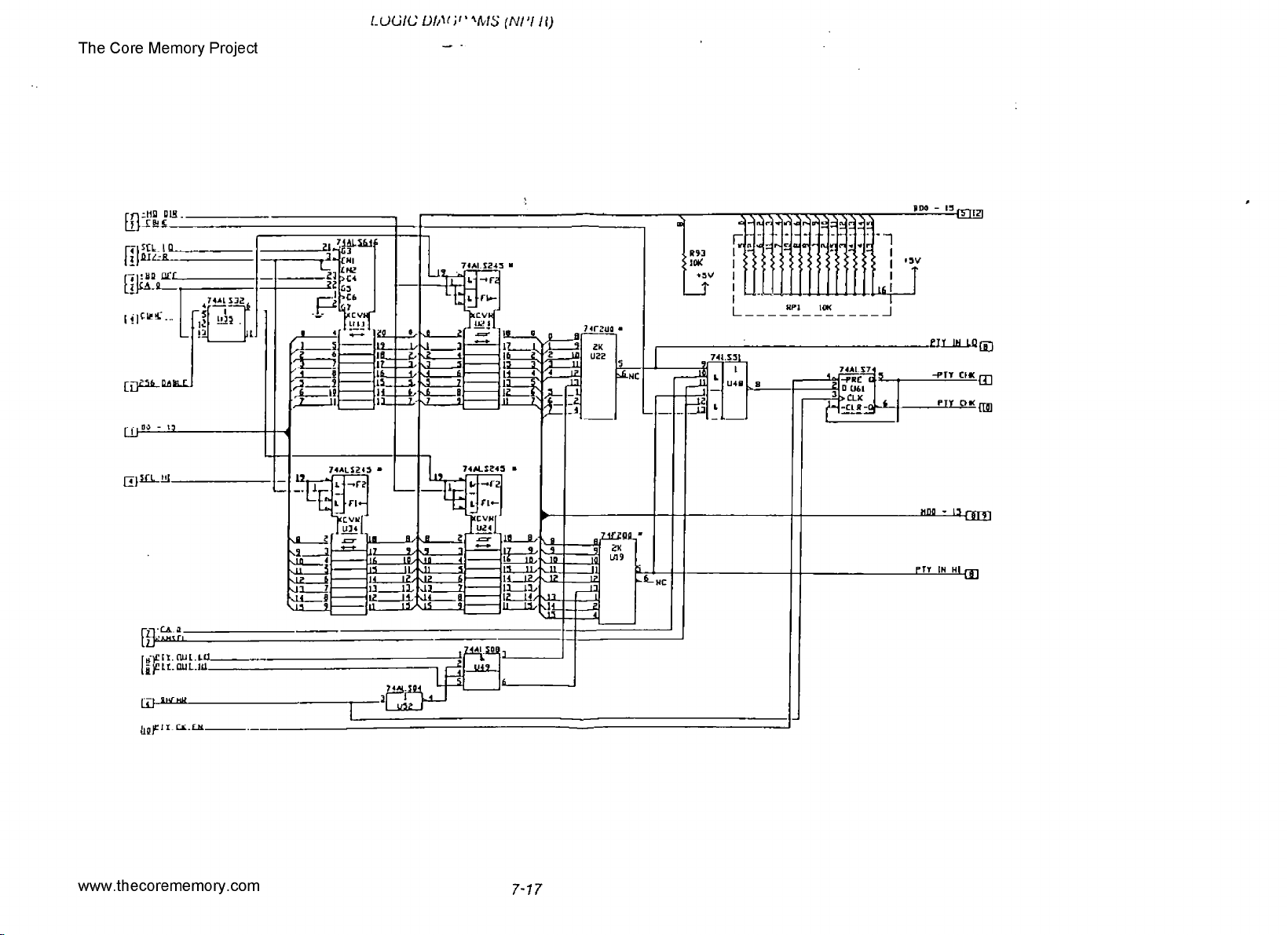
Page 77

Page 78

Page 79

Page 80

Page 81

Page 82

 Loading...