

Natlinear LN4890M, LN4890MM Schematics

LN4890
Rev.1.0 —Nov. 24, 2011
1
www.natlinear.com
Low-Cost, Mono/Stereo, 1 W Differential Audio Power Amplifiers
■ General Description
The LN4890 is an audio power amplifier primarily designed
for demanding applications in mobile phones and other
portable communication device applications. It is capable
of delivering 1 watt of continuous average power to an 8Ω
BTL load with less than 1% distortion (THD+N) from a 5V
DC power supply. Boomer audio power amplifiers were
designed specifically to provide high quality output power
with a minimal amount of external components. The
LN4890 does not require output coupling capacitors or
bootstrap capacitors, and therefore is ideally suited for
mobile phone and other low voltage applications where
minimal power consumption is a primary requirement.
The LN4890 features a low-power consumption shutdown
mode, which is achieved by driving the shutdown pin with
logic low. Additionally, the LN4890 features an internal
thermal shutdown protection mechanism. The LN4890
contains advanced pop & click circuitry which eliminates
noises which would otherwise occur during turn-on and
turn-off transitions. The LN4890 is unity-gain stable and
can be configured by external gain-setting resistors.
■ Key Specifications
PSRR @fIN=217Hz, VDD = 5V 62dB(typ.)
Power Output@VDD= 5.0V &1% THD 1W(typ.)
Power Output @VDD=3.3V &1% THD 400mW(typ.)
Shutdown Current 0.1μA(typ.)
■ Features
Available in space-saving packages
Ultra low current shutdown mode
BTL output can drive capacitive loads
Improved pop & click circuitry eliminates noises
during turn-on and turn-off transitions
2.2 - 5.0V operation
No output coupling capacitors, snubber networks or
bootstrap capacitors required
Thermal shutdown protection
Unity-gain stable
External gain configuration capability
■ Applications
Mobile Phones
PDAs
Portable electronic devices
■ Package
MSOP-8
SOP-8
■ Ordering Information
LN4890XY
项目
符号
描述
X
Package Type :
MM
MSOP-8
M
SOP-8
Y
A
When the input is greater than 5.2V IC will automatically shut down
C
No high voltage automatic closing function
D
No high voltage automatic closing function, and under the high pressure,
the gain will be automatically reduced to 1 times
LN4890
Rev.1.0 —Nov. 24, 2011
2
www.natlinear.com
■ Operating Ratings
Temperature Range
TMIN ≤ TA ≤ TMAX----------------------------------------------------------------------------------------------------- −40°C ≤ TA ≤ 85°C
Supply Voltage ------------------------------------------------------------------------------------------------------------ 2.2V ≤ VDD ≤ 5.0V
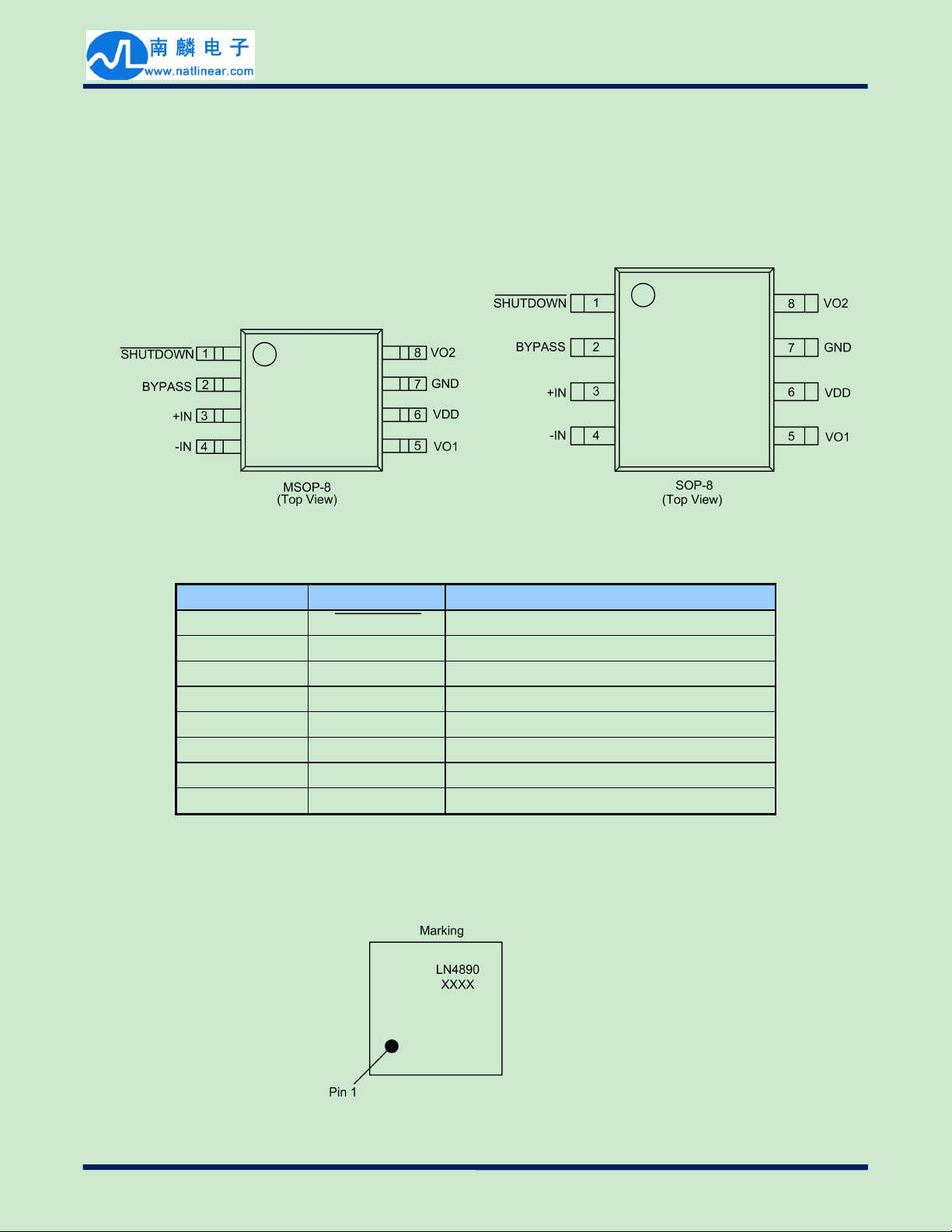
■ Pin Configuration
■ Pin Function Description
Pin Number
Pin Name
Function Description
1
SHUTDOWN
Chip Enable (Low Effective)
2
BYPASS
Bypass Capacitance Input Pin
3
+IN
Positive Input Terminal (Differential +)
4
-IN
Negative Input Terminal (Differential -)
5
VO1
Negative Output Terminal (Differential -)
6
VDD
Power Supply
7
GND
Ground Pin
8
VO2
Positive Output Terminal (Differential +)
■ Marking Rule
MSOP-8、SOP-8
XXXX: Date Code
LN4890
Rev.1.0 —Nov. 24, 2011
3
www.natlinear.com
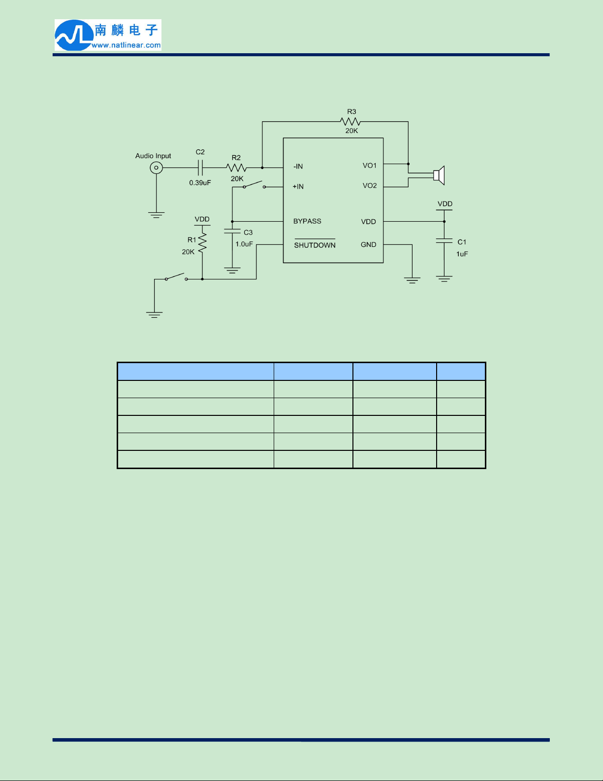
■ Typical Application Circuit
■ Absolute Maximum Ratings
Parameter
Symbol
Value
Unit
Supply Voltage
VDD-0.3—5.0
V
Input Voltage
V
IN
-0.3—VDD+0.3
V
Operation Temperature
Topr
-40—85
℃
Storage Temperature
Tstg
-65—150
℃
ESD Susceptibility
-
2000
V
LN4890
Rev.1.0 —Nov. 24, 2011
4
www.natlinear.com
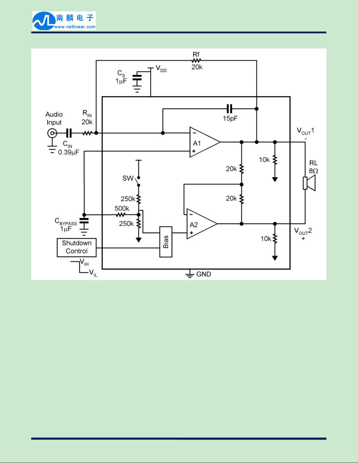
■ Function Block Diagram

LN4890
Rev.1.0 —Nov. 24, 2011
5
www.natlinear.com
■ Electrical Characteristics
(VDD = 5V Unless otherwise specified. Limits apply for TA = 25°C.)
Parameter
Symbol
Condition
Min
Typ
Max
Unit
I
DD
Quiescent Power
Supply Current
VIN = 0V, Io = 0A, No Load
—48
mA
VIN = 0V, Io = 0A, 8Ω Load
—510
mA
ISDShutdown Current
V
SHUTDOWN
= 0V
—
0.12μA
V
SDIH
Shutdown Voltage
Input High
1.2——
V
V
SDIL
Shutdown Voltage
Input Low
——0.4
V
V
OS
Output Offset Voltage
—750
mV
R
OUT-GND
Resistor Output
to GND
7.0
8.5
9.7
kΩ
P
O
Output Power ( 8Ω )
THD = 2% (max);
f = 1 kHz 8Ω Load
0.8
1.0—W
TWUWake-up time
—
170
220
ms
T
SD
Thermal Shutdown
Temperature
150
170
190
℃
THD+N
Total Harmonic
Distortion+Noise
Po = 0.4 Wrms; f = 1kHz
—
0.1—%
PSRR
Power Supply
Rejection Ratio
V
ripple
= 200mV
sine p-p
f=217Hz
5562—
dB
V
ripple
= 200mV
sine p-p
f=1kHz
66
T
SDT
Shut Down Time
8Ω Load
—
1.0—ms
 Loading...