

查询TP3052-X供应商
TP3054-X, TP3057-X
Extended Temperature Serial Interface CODEC/Filter
COMBO
®
Family
TP3054-X, TP3057-X Extended Temperature Serial Interface CODEC/Filter COMBO Family
March 2005
General Description
The TP3054, TP3057 family consists of µ-law and A-law
monolithic PCM CODEC/filters utilizing the A/D and D/A
conversion architecture shown in Figure 1, and a serial PCM
interface. The devices are fabricated using National’s advanced double-poly CMOS process (microCMOS).
The encode portion of each device consists of an input gain
adjust amplifier, an active RC pre-filter which eliminates very
high frequency noise prior to entering a switched-capacitor
band-pass filter that rejects signals below 200 Hz and above
3400 Hz. Also included are auto-zero circuitry and a companding coder which samples the filtered signal and encodes it in the companded µ-law or A-law PCM format. The
decode portion of each device consists of an expanding
decoder, which reconstructs the analog signal from the companded µ-law or A-law code, a low-pass filter which corrects
for the sin x/x response of the decoder output and rejects
signals above 3400 Hz followed by a single-ended power
amplifier capable of driving low impedance loads. The devices require two 1.536 MHz, 1.544 MHz or 2.048 MHz
transmit and receive master clocks, which may be asynchronous; transmit and receive bit clocks, which may vary from
64 kHz to 2.048 MHz; and transmit and receive frame sync
pulses. The timing of the frame sync pulses and PCM data is
compatible with both industry standard formats.
Connection Diagrams
Features
n −40˚C to +85˚C operation
n Complete CODEC and filtering system (COMBO)
including:
— Transmit high-pass and low-pass filtering
— Receive low-pass filter with sin x/x correction
— Active RC noise filters
— µ-law or A-law compatible COder and DECoder
— Internal precision voltage reference
— Serial I/O interface
— Internal auto-zero circuitry
n µ-law, 16-pin —TP3054
n A-law, 16-pin —TP3057
n Designed for D3/D4 and CCITT applications
±
n
5V operation
n Low operating power —typically 50 mW
n Power-down standby mode —typically 3 mW
n Automatic power-down
n TTL or CMOS compatible digital interfaces
n Maximizes line interface card circuit density
n Dual-In-Line or PCC surface mount packages
n See also AN-370, “Techniques for Designing with
CODEC/Filter COMBO Circuits”
Plastic Chip Carriers
00867408
Top View
Order Number TP3057V-X
NS Package Number V20A
COMBO®and TRI-STATE®are registered trademarks of National Semiconductor Corporation.
© 2005 National Semiconductor Corporation DS008674 www.national.com
Dual-In-Line Package
00867401
Top View
Order Number TP3054N-X
NS Package Number N16E
Order Number TP3054WM-X
NS Package Number M16B
Block Diagram
TP3054-X, TP3057-X
Pin Descriptions
Symbol Function
V
BB
GNDA Analog ground. All signals are
VF
O Analog output of the receive power
R
V
CC
FS
R
D
R
Negative power supply pin.
V
= −5V±5%.
BB
referenced to this pin.
amplifier.
Positive power supply pin.
V
= +5V±5%.
CC
Receive frame sync pulse which
enables BCLK
.FSRis an 8 kHz pulse train. See
D
R
to shift PCM data into
R
Figure 2 and Figure 3 for timing details.
Receive data input. PCM data is shifted
following the FSRleading edge.
into D
R
FIGURE 1.
Symbol Function
BCLK
/CLKSEL The bit clock which shifts data into D
R
after the FSRleading edge. May vary
from 64 kHz to 2.048 MHz.
Alternatively, may be a logic input
which selects either 1.536 MHz/1.544
MHz or 2.048 MHz for master clock in
synchronous mode and BCLK
for both transmit and receive directions
(see Table 1).
/PDN Receive master clock. Must be 1.536
MCLK
R
MHz, 1.544 MHz or 2.048 MHz. May be
asynchronous with MCLK
be synchronous with MCLK
performance. When MCLK
connected continuously low, MCLK
selected for all internal timing. When
MCLK
is connected continuously high,
R
the device is powered down.
00867402
is used
X
, but should
X
for best
X
is
R
R
is
X
www.national.com 2
Pin Descriptions (Continued)
Symbol Function
MCLK
X
Transmit master clock. Must be 1.536
MHz, 1.544 MHz or 2.048 MHz. May be
asynchronous with MCLK
. Best
R
performance is realized from
synchronous operation.
FS
X
Transmit frame sync pulse input which
enables BCLK
data on D
to shift out the PCM
X
.FSXis an 8 kHz pulse
X
train, see Figure 2 and Figure 3 for
timing details.
BCLK
X
The bit clock which shifts out the PCM
data on D
. May vary from 64 kHz to
X
2.048 MHz, but must be synchronous
.
X
.
X
D
TS
with MCLK
X
The TRI-STATE®PCM data output
which is enabled by FS
X
Open drain output which pulses low
during the encoder time slot.
GS
X
Analog output of the transmit input
amplifier. Used to externally set gain.
−
VFXI
Inverting input of the transmit input
amplifier.
+
VF
I
X
Non-inverting input of the transmit input
amplifier.
Functional Description
POWER-UP
When power is first applied, power-on reset circuitry initializes the COMBO and places it into a power-down state. All
non-essential circuits are deactivated and the D
outputs are put in high impedance states. To power-up the
device, a logical low level or clock must be applied to the
/PDN pin and FSXand/or FSRpulses must be
MCLK
R
present. Thus, 2 power-down control modes are available.
The first is to pull the MCLK
to hold both FS
and FSRinputs continuously low —the
X
/PDN pin high; the alternative is
R
device will power-down approximately 1 ms after the last
or FSRpulse. Power-up will occur on the first FSXor
FS
X
pulse. The TRI-STATE PCM data output, DX, will remain
FS
R
in the high impedance state until the second FS
SYNCHRONOUS OPERATION
For synchronous operation, the same master clock and bit
clock should be used for both the transmit and receive
directions. In this mode, a clock must be applied to MCLK
and the MCLKR/PDN pin can be used as a power-down
control. A low level on MCLK
/PDN powers up the device
R
and a high level powers down the device. In either case,
MCLK
will be selected as the master clock for both the
X
transmit and receive circuits.A bit clock must also be applied
to BCLK
and the BCLKR/CLKSEL can be used to select the
X
proper internal divider for a master clock of 1.536 MHz,
1.544 MHz or 2.048 MHz. For 1.544 MHz operation, the
device automatically compensates for the 193rd clock pulse
each frame.
and VFRO
X
pulse.
X
TP3054-X, TP3057-X
With a fixed level on the BCLK
selected as the bit clock for both the transmit and receive
directions. Table 1 indicates the frequencies of operation
which can be selected, depending on the state of BCLK
CLKSEL. In this synchronous mode, the bit clock, BCLK
may be from 64 kHz to 2.048 MHz, but must be synchronous
with MCLK
Each FS
.
X
pulse begins the encoding cycle and the PCM
X
data from the previous encode cycle is shifted out of the
enabled D
output on the positive edge of BCLKX. After 8 bit
X
clock periods, the TRI-STATE D
impedance state. With an FS
via the D
input on the negative edge of BCLKX(or BCLK
R
if running). FSXand FSRmust be synchronous with
X/R
.
MCLK
TABLE 1. Selection of Master Clock Frequencies
BCLKR/CLKSEL
Clocked 2.048 MHz 1.536 MHz or
0 1.536 MHz or 2.048 MHz
1 2.048 MHz 1.536 MHz or
ASYNCHRONOUS OPERATION
For asynchronous operation, separate transmit and receive
clocks may be applied. MCLK
2.048 MHz for the TP3057, or 1.536 MHz, 1.544 MHz for the
TP3054, and need not be synchronous. For best transmission performance, however, MCLK
with MCLK
, which is easily achieved by applying only static
X
logic levels to the MCLK
connect MCLK
to all internal MCLKRfunctions (see Pin
X
Description). For 1.544 MHz operation, the device automatically compensates for the 193rd clock pulse each frame.
starts each encoding cycle and must be synchronous
FS
X
with MCLK
and BCLKX.FSRstarts each decoding cycle
X
and must be synchronous with BCLK
clock, the logic levels shown in Table 1 are not valid in
asynchronous mode. BCLK
64 kHz to 2.048 MHz.
SHORT FRAME SYNC OPERATION
The COMBO can utilize either a short frame sync pulse or a
long frame sync pulse. Upon power initialization, the device
assumes a short frame mode. In this mode, both frame sync
pulses, FS
X
timing relationships specified in Figure 2. With FS
during a falling edge of BCLK
BCLK
and FSR, must be one bit clock period long, with
X
enables the DXTRI-STATE output buffer, which will
X
output the sign bit. The following seven rising edges clock
out the remaining seven bits, and the next falling edge
disables the D
of BCLK
edge of BCLK
output. With FSRhigh during a falling edge
X
(BCLKXin synchronous mode), the next falling
R
latches in the sign bit. The following seven
R
falling edges latch in the seven remaining bits. All four devices may utilize the short frame sync pulse in synchronous
or asynchronous operating mode.
/CLKSEL pin, BCLKXwill be
R
output is returned to a high
X
pulse, PCM data is latched
R
Master Clock
Frequency Selected
TP3057 TP3054
1.544 MHz
1.544 MHz
1.544 MHz
and MCLKRmust be
X
should be synchronous
R
/PDN pin. This will automatically
R
. BCLKRmust be a
R
and BCLKRmay operate from
X
, the next rising edge of
X
X
high
/
R
,
X
R
www.national.com3

Functional Description (Continued)
LONG FRAME SYNC OPERATION
To use the long frame mode, both the frame sync pulses,
FS
and FSR, must be three or more bit clock periods long,
X
with timing relationships specified in Figure 3. Based on the
transmit frame sync, FS
short or long frame sync pulses are being used. For 64 kHz
TP3054-X, TP3057-X
operation, the frame sync pulse must be kept low for a
minimum of 160 ns. The D
enabled with the rising edge of FS
, whichever comes later, and the first bit clocked out
BCLK
X
is the sign bit. The following seven BCLK
out the remaining seven bits. The D
the falling BCLK
going low, whichever comes later. A rising edge on the
FS
X
edge following the eighth rising edge, or by
X
receive frame sync pulse, FS
to be latched in on the next eight falling edges of BCLK
D
R
(BCLKXin synchronous mode). All four devices may utilize
the long frame sync pulse in synchronous or asynchronous
mode.
In applications where the LSB bit is used for signalling, with
two bit clock periods long, the decoder will interpret the
FS
R
lost LSB as “
1
⁄2” to minimize noise and distortion.
TRANSMIT SECTION
The transmit section input is an operational amplifier with
provision for gain adjustment using two external resistors,
see Figure 4. The low noise and wide bandwidth allow gains
in excess of 20 dB across the audio passband to be realized.
The op amp drives a unity-gain filter consisting of RC active
, the COMBO will sense whether
X
TRI-STATE output buffer is
X
R
or the rising edge of
X
rising edges clock
X
output is disabled by
X
, will cause the PCM data at
pre-filter, followed by an eighth order switched-capacitor
bandpass filter clocked at 256 kHz. The output of this filter
directly drives the encoder sample-and-hold circuit. The A/D
is of companding type according to µ-law (TP3054) or A-law
(TP3057) coding conventions. A precision voltage reference
is trimmed in manufacturing to provide an input overload
) of nominally 2.5V peak (see table of Transmission
(t
MAX
Characteristics). The FS
frame sync pulse controls the
X
sampling of the filter output, and then the successiveapproximation encoding cycle begins. The 8-bit code is then
loaded into a buffer and shifted out through D
pulse. The total encoding delay will be approximately
FS
X
at the next
X
165 µs (due to the transmit filter) plus 125 µs (due to encoding delay), which totals 290 µs. Any offset voltage due to the
filters or comparator is cancelled by sign bit integration.
RECEIVE SECTION
R
The receive section consists of an expanding DAC which
drives a fifth order switched-capacitor low pass filter clocked
at 256 kHz. The decoder is A-law (TP3057) or µ-law
(TP3054) and the 5th order low pass filter corrects for the sin
x/x attenuation due to the 8 kHz sample/hold. The filter is
then followed by a 2nd order RC active post-filter/power
amplifier capable of driving a 600Ω load to a level of 7.2
dBm. The receive section is unity-gain. Upon the occurrence
, the data at the DRinput is clocked in on the falling
of FS
R
edge of the next eight BCLK
(BCLKX) periods. At the end of
R
the decoder time slot, the decoding cycle begins, and 10 µs
later the decoder DAC output is updated. The total decoder
delay is ∼10 µs (decoder update) plus 110 µs (filter delay)
plus 62.5 µs (
1
⁄2frame), which gives approximately 180 µs.
www.national.com 4
TP3054-X, TP3057-X
Absolute Maximum Ratings (Note 1)
If Military/Aerospace specified devices are required,
please contact the National Semiconductor Sales Office/
Distributors for availability and specifications.
to GNDA 7V
V
CC
V
to GNDA −7V
BB
Voltage at any Digital Input or
Output V
+0.3V to GNDA−0.3V
CC
Operating Temperature Range −55˚C to + 125˚C
Storage Temperature Range −65˚C to +150˚C
Lead Temperature
(Soldering, 10 sec.) 300˚C
Voltage at any Analog Input
or Output V
+0.3V to VBB−0.3V
CC
Electrical Characteristics
Unless otherwise noted, limits printed in BOLD characters are guaranteed for VCC= +5.0V±5%, VBB= −5.0V±5%; TA=
−40˚C to +85˚C by correlation with 100% electrical testing at T
production tests and/or product design and characterization. All signals referenced to GNDA. Typicals specified at V
+5.0V, V
= −5.0V, TA= 25˚C.
BB
Symbol Parameter Conditions Min Typ Max Units
DIGITAL INTERFACE
V
IL
V
IH
V
OL
V
OH
I
IL
I
IH
I
OZ
Input Low Voltage 0.6 V
Input High Voltage 2.2 V
Output Low Voltage DX,IL=3.2 mA 0.4 V
SIG
R,IL
TS
X,IL
Output High Voltage DX,IH=−3.2 mA 2.4 V
SIG
R,IH
Input Low Current GNDA≤VIN≤VIL, All Digital Inputs −10 10 µA
Input High Current VIH≤VIN≤V
Output Current in High Impedance DX, GNDA≤VO≤V
State (TRI-STATE)
ANALOG INTERFACE WITH TRANSMIT INPUT AMPLIFIER (ALL DEVICES)
I
XA Input Leakage Current −2.5V≤V≤+2.5V, VFXI+or VFXI
I
R
XA Input Resistance −2.5V≤V≤+2.5V, VFXI+or VFXI
I
R
XA Output Resistance Closed Loop, Unity Gain 1 3 Ω
O
R
XA Load Resistance GS
L
C
XA Load Capacitance GS
L
V
XA Output Dynamic Range GSX,RL≥ 10 kΩ −2.8 2.8 V
O
A
XA Voltage Gain VFXI+to GS
V
F
XA Unity Gain Bandwidth 1 2 MHz
U
V
XA Offset Voltage −20 20 mV
OS
V
XA Common-Mode Voltage CMRRXA>60 dB −2.5 2.5 V
CM
X
X
CMRRXA Common-Mode Rejection Ratio DC Test 60 dB
PSRRXA Power Supply Rejection Ratio DC Test 60 dB
ANALOG INTERFACE WITH RECEIVE FILTER (ALL DEVICES)
R
RF Output Resistance Pin VFRO13Ω
O
R
RF Load Resistance VFRO=±2.5V 600 Ω
L
C
RF Load Capacitance 500 pF
L
VOS
O Output DC Offset Voltage −200 200 mV
R
POWER DISSIPATION (ALL DEVICES)
I
0 Power-Down Current No Load (Note 2) 0.65 2.0 mA
CC
I
0 Power-Down Current No Load (Note 2) 0.01 0.33 mA
BB
I
1 Power-Up (Active) Current No Load( –40˚C to 85˚C) 5.0 11.0 mA
CC
I
1 Power-Up (Active) Current No Load ( –40˚C to 85˚C) 5.0 11.0 mA
BB
Note 1: “Absolute Maximum Ratings” indicate limits beyond which damage to the device may occur. Operating Ratings indicate conditions for which the device is
functional, but do not guarantee specific performance limits.
Note 2: I
CC0
and I
are measured after first achieving a power-up state.
BB0
= 25˚C. All other limits are assured by correlation with other
A
=
CC
=1.0 mA 0.4 V
=3.2 mA, Open Drain 0.4 V
=−1.0 mA 2.4 V
CC
CC
−
−
−10 10 µA
−10 10 µA
−200 200 nA
10 MΩ
10 kΩ
50 pF
X
5000 V/V
www.national.com5

Timing Specifications
Unless otherwise noted, limits printed in BOLD characters are guaranteed for VCC= +5.0V±5%, VBB= −5.0V±5%; TA=
−40˚C to +85˚C by correlation with 100% electrical testing at T
production tests and/or product design and characterization. All signals referenced to GNDA. Typicals specified at V
+5.0V, V
= – 5.0V, TA= 25˚C. All timing parameters are assured at VOH= 2.0V and VOL= 0.7V. See Definitions and Timing
BB
Conventions section for test methods information.
Symbol Parameter Conditions Min Typ Max Units
TP3054-X, TP3057-X
1/t
PM
t
RM
t
FM
t
PB
t
RB
t
FB
t
WMH
t
WML
t
SBFM
t
SFFM
t
WBH
t
WBL
t
HBFL
Frequency of Master Clocks Depends on the Device Used and the 1.536 MHz
BCLK
/CLKSEL Pin. 1.544 MHz
R
MCLK
X
Rise Time of Master Clock MCLKXand MCLK
Fall Time of Master Clock MCLKXand MCLK
Period of Bit Clock 485 488 15725 ns
Rise Time of Bit Clock BCLKXand BCLK
Fall Time of Bit Clock BCLKXand BCLK
Width of Master Clock High MCLKXand MCLK
Width of Master Clock Low MCLKXand MCLK
Set-Up Time from BCLKXHigh First Bit Clock after Short Frame 100 ns
to MCLK
Setup Time from FSXHigh to
MCLK
Falling Edge the Leading Edge
X
of FS
X
Long Frame Only 100 ns
Falling Edge
X
Width of Bit Clock High VIH=2.2V 160 ns
Width of Bit Clock Low VIL=0.6V 160 ns
Holding Time from Bit Clock Long Frame Only 0 ns
Low to Frame Sync
t
HBFS
Holding Time from Bit Clock Short Frame Only 0 ns
High to Frame Sync
t
SFB
Set-Up Time from Frame Sync Long Frame Only 115 ns
to Bit Clock Low
t
DBD
Delay Time from BCLKXHigh Load=150 pF plus 2 LSTTL Loads 0 140 ns
to Data Valid
t
DBTS
t
DZC
Delay Time to TSXLow Load=150 pF plus 2 LSTTL Loads 140 ns
Delay Time from BCLKXLow to CL=0 pF to 150 pF 50 165 ns
Data Output Disabled
t
DZF
Delay Time to Valid Data from CL=0 pF to 150 pF 20 165 ns
FS
or BCLKX, Whichever
X
Comes Later
t
t
t
t
t
SDB
HBD
SF
HF
HBFl
Set-Up Time from DRValid to 50 ns
BCLK
Hold Time from BCLK
D
Set-Up Time from FS
BCLK
Hold Time from BCLK
to FS
Low
R/X
Low to 50 ns
R/X
Invalid
R
to Short Frame Sync Pulse (1 Bit Clock 50 ns
X/R
Low Period Long)
X/R
Low Short Frame Sync Pulse (1 Bit Clock 100 ns
X/R
Low Period Long)
X/R
Hold Time from 3rd Period of Long Frame Sync Pulse (from 3 to 8 Bit 100 ns
Bit Clock Low to Frame Sync Clock Periods Long)
(FS
or FSR)
X
t
WFL
Minimum Width of the Frame 64k Bit/s Operating Mode 160 ns
Sync Pulse (Low Level)
= 25˚C. All other limits are assured by correlation with other
A
and MCLK
R
R
R
R
R
R
R
160 ns
160 ns
2.048 MHz
Long Frame 125
=
CC
50 ns
50 ns
50 ns
50 ns
www.national.com 6

00867403
TP3054-X, TP3057-X
Timing Diagrams
FIGURE 2. Short Frame Sync Timing
www.national.com7

TP3054-X, TP3057-X
00867409
Timing Diagrams (Continued)
FIGURE 3. Long Frame Sync Timing
www.national.com 8
Transmission Characteristics
Unless otherwise noted, limits printed in BOLD characters are guaranteed for VCC= +5.0V±5%, VBB= −5.0V±5%; TA=
−40˚C to +85˚C by correlation with 100% electrical testing at T
production tests and/or product design and characterization. GNDA = 0V, f = 1.02 kHz, V
connected for unity gain non inverting. Typicals are specified at V
Symbol Parameter Conditions Min Typ Max Units
AMPLITUDE RESPONSE
Absolute Levels Nominal 0 dBm0 Level is 4 dBm
(Definition of nominal gain) (600Ω)
0 dBm0 1.2276 Vrms
t
MAX
Max Overload Level
TP3054 (3.17 dBm0) 2.501 V
TP3057 (3.14 dBm0) 2.492 V
G
XA
Transmit Gain, Absolute TA=25˚C, VCC=5V, VBB=−5V
Input at GS
G
XR
Transmit Gain, Relative to G
XA
f=16 Hz −40 dB
f=50 Hz −30 dB
f=60 Hz −26 dB
f=200 Hz −1.8 −0.1 dB
f=300 Hz– 3000 Hz −0.15 0.15 dB
f=3152 Hz −0.15 0.20 dB
f=3300 Hz −0.35 0.1 dB
f=3400 Hz −0.7 0 dB
f=4000 Hz −14 dB
f=4600 Hz and Up, Measure −32 dB
Response from 0 Hz to 4000 Hz
G
XAT
Absolute Transmit Gain Variation Relative to G
with Temperature
G
XAV
Absolute Transmit Gain Variation Relative to G
with Supply Voltage
G
XRL
Transmit Gain Variations with Sinusoidal Test Method
Level Reference Level=−10 dBm0
VF
I+=−40 dBm0 to +3 dBm0 −0.2 0.2 dB
X
VF
I+=−50 dBm0 to −40 dBm0 −0.4 0.4 dB
X
VF
I+=−55 dBm0 to −50 dBm0 −1.2 1.2 dB
X
G
RA
Receive Gain, Absolute TA=25˚C, VCC=5V, VBB=−5V
Input=Digital Code Sequence
for 0 dBm0 Signal at 1020 Hz −0.20 0.20 dB
G
RR
Receive Gain, Relative to G
RA
f=0 Hz to 3000 Hz −0.15 0.15 dB
f=3300 Hz −0.35 0.1 dB
f=3400 Hz −0.7 0 dB
f=4000 Hz −14 dB
G
RAT
Absolute Receive Gain Variation Relative to G
with Temperature
G
RAV
Absolute Receive Gain Variation Relative to G
with Supply Voltage
G
RRL
Receive Gain Variations with Sinusoidal Test Method; Reference
Level Input PCM Code Corresponds to an
Ideally Encoded
PCM Level =−40 dBm0 to +3 dBm0 −0.2 0.2 dB
PCM Level =−50 dBm0 to −40 dBm0 −0.4 0.4 dB
PCM Level =−55 dBm0 to −50 dBm0 −1.2 1.2 dB
= 25˚C. All other limits are assured by correlation with other
A
= +5.0V, VBB= −5.0V, TA= 25˚C.
CC
=0 dBm0 at 1020 Hz −0.15 0.15 dB
x
XA
XA
RA
RA
= 0 dBm0, transmit input amplifier
IN
−0.15 0.15 dB
−0.05 0.05 dB
−0.15 0.15 dB
−0.05 0.05 dB
TP3054-X, TP3057-X
PK
PK
www.national.com9

Transmission Characteristics (Continued)
Unless otherwise noted, limits printed in BOLD characters are guaranteed for VCC= +5.0V±5%, VBB= −5.0V±5%; TA=
−40˚C to +85˚C by correlation with 100% electrical testing at T
production tests and/or product design and characterization. GNDA = 0V, f = 1.02 kHz, V
connected for unity gain non inverting. Typicals are specified at V
Symbol Parameter Conditions Min Typ Max Units
AMPLITUDE RESPONSE
TP3054-X, TP3057-X
V
RO
Receive Output Drive Level RL=600Ω −2.5 2.5 V
ENVELOPE DELAY DISTORTION WITH FREQUENCY
D
XA
D
XR
Transmit Delay, Absolute f=1600 Hz 290 315 µs
Transmit Delay, Relative to D
XA
f=500 Hz−600 Hz 195 220 µs
f=600 Hz−800 Hz 120 145 µs
f=800 Hz−1000 Hz 50 75 µs
f=1000 Hz−1600 Hz 20 40 µs
f=1600 Hz−2600 Hz 55 75 µs
f=2600 Hz−2800 Hz 80 105 µs
f=2800 Hz−3000 Hz 130 155 µs
D
RA
D
RR
Receive Delay, Absolute f=1600 Hz 180 200 µs
Receive Delay, Relative to D
RA
f=500 Hz−1000 Hz −40 −25 µs
f=1000 Hz−1600 Hz −30 −20 µs
f=1600 Hz−2600 Hz 70 90 µs
f=2600 Hz−2800 Hz 100 125 µs
f=2800 Hz−3000 Hz 145 175 µs
NOISE
N
XC
Transmit Noise, C Message TP3054 12 16 dBrnC0
Weighted (Note 3)
N
XP
Transmit Noise, P Message TP3057 −74 −67 dBm0p
Weighted (Note 3)
N
RC
Receive Noise, C Message PCM Code is Alternating
Weighted Positive and Negative Zero — TP3054 8 11 dBrnC0
N
RP
Receive Noise, P Message TP3057 PCM Code Equals Positive
Weighted Zero — −82 −79 dBm0p
N
RS
Noise, Single Frequency f=0 kHz to 100 kHz, Loop Around −53 dBm0
Measurement, VF
PPSR
Positive Power Supply Rejection, VCC=5.0 VDC+100 mVrms
X
Transmit f=0 kHz−50 kHz (Note 4) 40 dBC
NPSR
Negative Power Supply Rejection, VBB=−5.0 VDC+ 100 mVrms
X
Transmit f=0 kHz−50 kHz (Note 4) 40 dBC
PPSR
Positive Power Supply Rejection, PCM Code Equals Positive Zero
R
Receive V
=5.0 VDC+100 mVrms
CC
Measure VF
f=0 Hz−4000 Hz 38 dBC
f=4 kHz−25 kHz 38 dB
f=25 kHz−50 kHz 35 dB
NPSR
Negative Power Supply Rejection, PCM Code Equals Positive Zero
R
Receive V
=−5.0 VDC+100 mVrms
BB
Measure VF
f=0 Hz−4000 Hz 38 dBC
f=4 kHz−25 kHz 38 dB
f=25 kHz−50 kHz 35 dB
= 25˚C. All other limits are assured by correlation with other
R
R
A
= +5.0V, VBB= −5.0V, TA= 25˚C.
CC
I+=0 Vrms
X
0
0
= 0 dBm0, transmit input amplifier
IN
www.national.com 10

Transmission Characteristics (Continued)
Unless otherwise noted, limits printed in BOLD characters are guaranteed for VCC= +5.0V±5%, VBB= −5.0V±5%; TA=
−40˚C to +85˚C by correlation with 100% electrical testing at T
production tests and/or product design and characterization. GNDA = 0V, f = 1.02 kHz, V
connected for unity gain non inverting. Typicals are specified at V
Symbol Parameter Conditions Min Typ Max Units
NOISE
SOS Spurious Out-of-Band Signals Loop Around Measurement, 0 dBm0, −30 dB
at the Channel Output 300 Hz to 3400 Hz Input PCM Code
Applied at D
4600 Hz– 7600 Hz −30 dB
7600 Hz– 8400 Hz −40 dB
8400 Hz– 100,000 Hz −30 dB
DISTORTION
STD
STD
Signal to Total Distortion Sinusoidal Test Method (Note 6)
X,
Transmit or Receive Level=3.0 dBm0 33 dBC
R
Half-Channel =0 dBm0 to −30 dBm0 36 dBC
=−40 dBm0 XMT 28 dBC
=−55 dBm0 XMT 13 dBC
SFD
Single Frequency Distortion, −43 dB
X
Transmit
SFD
Single Frequency Distortion, −43 dB
R
Receive
IMD Intermodulation Distortion Loop Around Measurement, −41 dB
VF
I+=−4 dBm0 to −21 dBm0, Two
X
Frequencies in the Range
300 Hz−3400 Hz
CROSSTALK
CT
CT
X-R
R-X
Transmit to Receive Crosstalk, f=300 Hz−3400 Hz −90 −70 dB
0 dBm0 Transmit Level D
=Quiet PCM Code (Note 6)
R
Receive to Transmit Crosstalk, f=300 Hz−3400 Hz, VFXI=Multitone −90 −70 dB
0 dBm0 Receive Level (Note 4)
= 25˚C. All other limits are assured by correlation with other
A
= +5.0V, VBB= −5.0V, TA= 25˚C.
CC
.
R
= 0 dBm0, transmit input amplifier
IN
RCV 29 dBC
RCV 14 dBC
TP3054-X, TP3057-X
ENCODING FORMAT AT DXOUTPUT
TP3054 TP3057
µ-Law A-Law
(Includes Even Bit Inversion)
V
(at GSX)=+Full-Scale 10000000 10101010
IN
V
(at GSX)=0V 11111111 11010101
IN
01111111 01010101
V
(at GSX)=−Full-Scale 00000000 00101010
IN
Note 3: Measured by extrapolation from the distortion test result at −50 dBm0.
Note 4: PPSR
Note 5: TP3054/57 are measured using C message weighted filter for µ-law and psophometric weighted filter for A-law.
Note 6: CT
, NPSRX, and CT
X
@
1.544 MHz MCLKXfreq. is −70 dB max. 50%±5% BCLKXduty cycle.
X–R
are measured with a −50 dBm0 activation signal applied to VFXI+.
R–X
www.national.com11

Applications Information
POWER SUPPLIES
While the pins of the TP3050 family are well protected
against electrical misuse, it is recommended that the standard CMOS practice be followed, ensuring that ground is
connected to the device before any other connections are
made. In applications where the printed circuit board may be
TP3054-X, TP3057-X
plugged into a “hot” socket with power and clocks already
present, an extra long ground pin in the connector should be
used.
All ground connections to each device should meet at a
common point as close as possible to the GNDA pin. This
minimizes the interaction of ground return currents flowing
through a common bus impedance. 0.1 µF supply decoupling capacitors should be connected from this common
ground point to V
possible.
For best performance, the ground point of each CODEC/
FILTER on a card should be connected to a common card
ground in star formation, rather than via a ground bus.
T-Pad Attenuator
and VBB, as close to device pins as
CC
This common ground point should be decoupled to V
with 10 µF capacitors.
V
BB
and
CC
RECEIVE GAIN ADJUSTMENT
For applications where a TP3050 family CODEC/filter receive output must drive a 600Ω load, but a peak swing lower
±
than
2.5V is required, the receive gain can be easily adjusted by inserting a matched T-pad or π-pad at the output.
Table 2 lists the required resistor values for 600Ω termina-
tions. As these are generally non-standard values, the equations can be used to compute the attenuation of the closest
practical set of resistors. It may be necessary to use unequal
values for the R1 or R4 arms of the attenuators to achieve a
precise attenuation. Generally it is tolerable to allow a small
deviation of the input impedance from nominal while still
maintaining a good return loss. For example a 30 dB return
loss against 600Ω is obtained if the output impedance of the
attenuator is in the range 282Ω to 319Ω (assuming a perfect
transformer).
00867411
www.national.com 12

Applications Information (Continued)
π-Pad Attenuator
TP3054-X, TP3057-X
Note: See Application Note 370 for further details.
00867412
TABLE 2. Attentuator Tables for Z1=Z2=300Ω
(All Values in Ω)
dB R1 R2 R3 R4
0.1 1.7 26k 3.5 52k
0.2 3.5 13k 6.9 26k
0.3 5.2 8.7k 10.4 17.4k
0.4 6.9 6.5k 13.8 13k
0.5 8.5 5.2k 17.3 10.5k
0.6 10.4 4.4k 21.3 8.7k
0.7 12.1 3.7k 24.2 7.5k
0.8 13.8 3.3k 27.7 6.5k
0.9 15.5 2.9k 31.1 5.8k
1.0 17.3 2.6l 34.6 5.2k
2 34.4 1.3k 70 2.6k
3 51.3 850 107 1.8k
4 68 650 144 1.3k
5 84 494 183 1.1k
6 100 402 224 900
7 115 380 269 785
8 379 284 317 698
9 143 244 370 630
10 156 211 427 527
11 168 184 490 535
12 180 161 550 500
13 190 142 635 473
14 200 125 720 450
15 210 110 816 430
16 218 98 924 413
18 233 77 1.17k 386
20 246 61 1.5k 366
www.national.com13
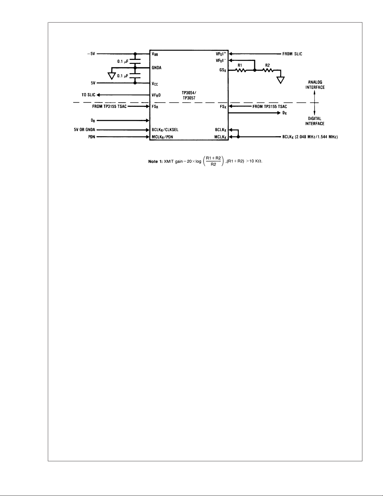
Typical Synchronous Application
TP3054-X, TP3057-X
00867406
FIGURE 4.
www.national.com 14

Physical Dimensions inches (millimeters)
unless otherwise noted
TP3054-X, TP3057-X
Dual-In-Line Package (M)
Order Number TP3054WM-X
NS Package Number M16B
Molded Dual-In-Line Package (N)
Order Number TP3054N-X
NS Package Number N16E
www.national.com15

Physical Dimensions inches (millimeters) unless otherwise noted (Continued)
Cavity Dual-In-Line Package (V)
Order Number TP3057V-X
NS Package Number V20A
National does not assume any responsibility for use of any circuitry described, no circuit patent licenses are implied and National reserves
the right at any time without notice to change said circuitry and specifications.
For the most current product information visit us at www.national.com.
LIFE SUPPORT POLICY
NATIONAL’S PRODUCTS ARE NOT AUTHORIZED FOR USE AS CRITICAL COMPONENTS IN LIFE SUPPORT DEVICES OR SYSTEMS
WITHOUT THE EXPRESS WRITTEN APPROVAL OF THE PRESIDENT AND GENERAL COUNSEL OF NATIONAL SEMICONDUCTOR
CORPORATION. As used herein:
1. Life support devices or systems are devices or systems
which, (a) are intended for surgical implant into the body, or
(b) support or sustain life, and whose failure to perform when
properly used in accordance with instructions for use
2. A critical component is any component of a life support
device or system whose failure to perform can be reasonably
expected to cause the failure of the life support device or
system, or to affect its safety or effectiveness.
provided in the labeling, can be reasonably expected to result
in a significant injury to the user.
BANNED SUBSTANCE COMPLIANCE
National Semiconductor manufactures products and uses packing materials that meet the provisions of the Customer Products
Stewardship Specification (CSP-9-111C2) and the Banned Substances and Materials of Interest Specification (CSP-9-111S2) and contain
no ‘‘Banned Substances’’ as defined in CSP-9-111S2.
TP3054-X, TP3057-X Extended Temperature Serial Interface CODEC/Filter COMBO Family
National Semiconductor
Americas Customer
Support Center
Email: new.feedback@nsc.com
Tel: 1-800-272-9959
www.national.com
National Semiconductor
Europe Customer Support Center
Fax: +49 (0) 180-530 85 86
Email: europe.support@nsc.com
Deutsch Tel: +49 (0) 69 9508 6208
English Tel: +44 (0) 870 24 0 2171
Français Tel: +33 (0) 1 41 91 8790
National Semiconductor
Asia Pacific Customer
Support Center
Email: ap.support@nsc.com
National Semiconductor
Japan Customer Support Center
Fax: 81-3-5639-7507
Email: jpn.feedback@nsc.com
Tel: 81-3-5639-7560
 Loading...