

查询SCAN182245A供应商
SCAN182245A
Non-Inverting Transceiver with
25X Series Resistor Outputs
SCAN182245A Transceiver with 25X Series Resistor Outputs
February 1996
General Description
The SCAN182245A is a high performance BiCMOS bidirectional line driver featuring separate data inputs organized
into dual 9-bit bytes with byte-oriented output enable and
direction control signals. This device is compliant with
IEEE 1149.1 Standard Test Access Port and Boundary
Scan Architecture with the incorporation of the defined
boundary-scan test logic and test access port consisting of
Test Data Input (TDI), Test Data Out (TDO), Test Mode Select (TMS), and Test Clock (TCK).
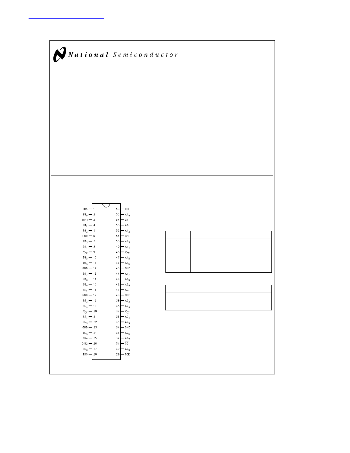
Connection Diagram
Features
Y
High performance BiCMOS technology
Y
25X series resistors in outputs eliminate the need for
external terminating resistors
Y
Dual output enable control signals
Y
TRI-STATEÉoutputs for bus-oriented applications
Y
25 mil pitch SSOP (Shrink Small Outline Package)
Y
IEEE 1149.1 (JTAG) Compliant
Y
Includes CLAMP, IDCODE and HIGHZ instructions
Y
Additional instructions SAMPLE-IN, SAMPLE-OUT and
EXTEST-OUT
Y
Power Up TRI-STATE for hot insert
Y
Member of National’s SCAN Products
Pin Names Description
A1
(0–8)
B1
(0–8)
A2
(0–8)
B2
(0–8)
G1
,G2 Output Enable Pins (Active Low)
DIR1, DIR2 Direction of Data Flow Pins
Side A1 Inputs or TRI-STATE Outputs
Side B1 Inputs or TRI-STATE Outputs
Side A2 Inputs or TRI-STATE Outputs
Side B2 Inputs or TRI-STATE Outputs
Order Number Description
SCAN182245ASSC SSOP in Tubes
SCAN182245ASSCX SSOP Tape and Reel
SCAN182245AFMQB Flatpak Military
TL/F/11657– 1
TRI-STATEÉis a registered trademark of National Semiconductor Corporation.
C
1996 National Semiconductor Corporation RRD-B30M36/Printed in U. S. A.
TL/F/11657
http://www.national.com
Truth Tables
Inputs
²
G1 DIR1
LL H
LL L
LH H
LH L
HX Z Z
A1
(0–8)B1(0–8)
w
w
x
x
H
L
H
L
Functional Description
The SCAN182245A consists of two sets of nine non-inverting bidirectional buffers with TRI-STATE outputs and is intended for bus-oriented applications. Direction pins (DIR1
and DIR2) LOW enables data from B ports to A ports, when
HIGH enables data from A ports to B ports. The Output
Enable pins (G1
ports by placing them in a high impedance condition.
and G2) when HIGH disables both A and B
Inputs
²
G2 DIR2
LL H
LL L
LH H
LH L
HX Z Z
e
H
HIGH Voltage Level
e
LOW Voltage Level
L
e
Immaterial
X
e
High Impedance
Z
e
²
Inactive-to-Active transition must occur to enable outputs upon
power-up.
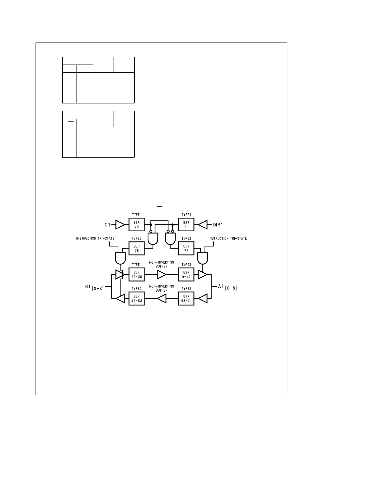
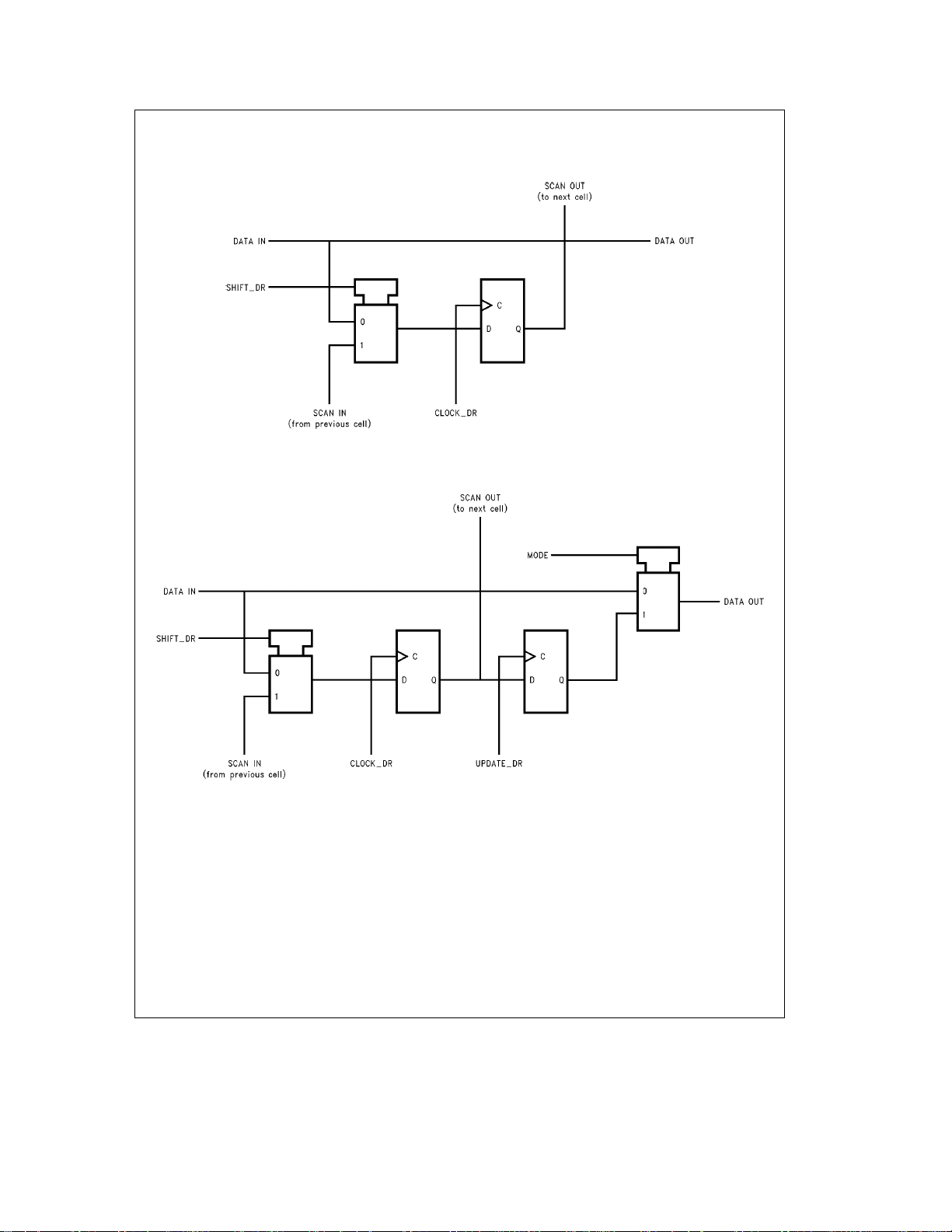
Block Diagrams
A2
(0–8)B2(0–8)
w
w
x
x
H
L
H
L
A1, B1, G1 and DIR1
Note: BSR stands for Boundary Scan Register.
http://www.national.com 2
TL/F/11657– 2
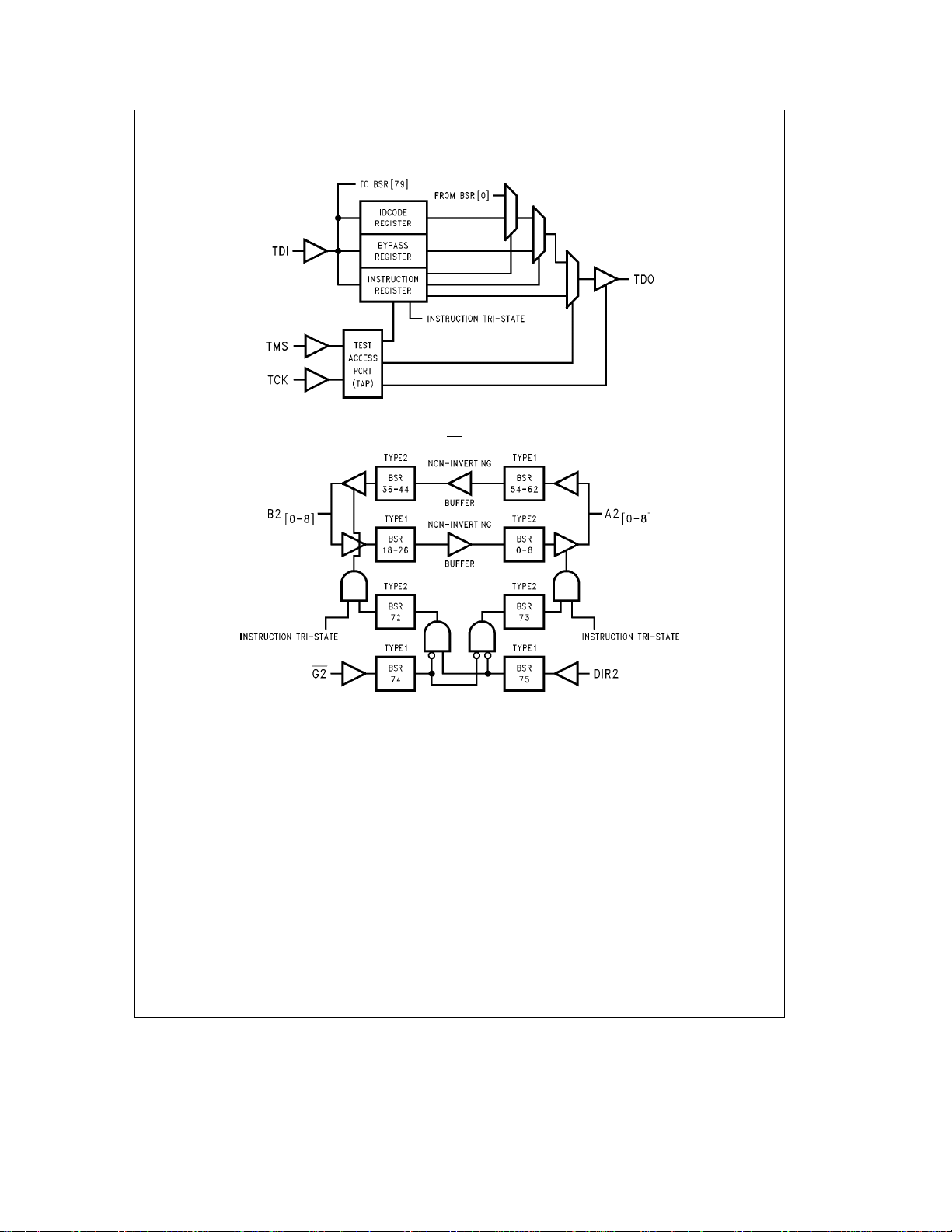
Block Diagrams (Continued)
Tap Controller
TL/F/11657– 18
A2, B2, G2 and DIR2
Note: BSR stands for Boundary Scan Register.
TL/F/11657– 3
http://www.national.com3
Description of BOUNDARY-SCAN Circuitry
The scan cells used in the BOUNDARY-SCAN register are
one of the following two types depending upon their location. Scan cell TYPE1 is intended to solely observe system
data, while TYPE2 has the additional ability to control system data. (See IEEE Standard 1149.1
further description of scan cell TYPE1 and
a further description of scan cell TYPE2.)
Scan cell TYPE1 is located on each system input pin while
scan cell TYPE2 is located at each system output pin as
well as at each of the two internal active-high output enable
signals. AOE controls the activity of the A-outputs while
BOE controls the activity of the B-outputs. Each will activate
their respective outputs by loading a logic high.
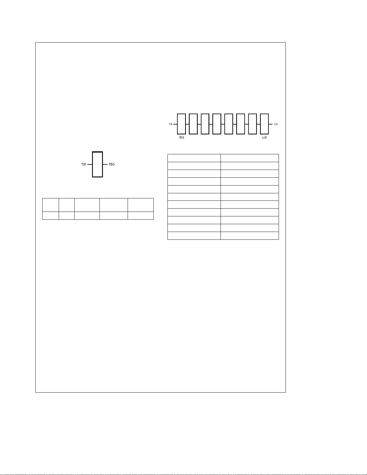
The BYPASS register is a single bit shift register stage identical to scan cell TYPE1. It captures a fixed logic low.
Bypass Register Scan Chain Definition
SCAN182245A Product IDCODE
(32-Bit Code per IEEE 1149.1)
Version Entity
0000 111111 0000000000 00000001111 1
MSB LSB
Logic 0
Part Manufacturer Required by
Number ID 1149.1
Figure 10-11
Figure 10-12
TL/F/11657– 17
for a
for
The INSTRUCTION register is an 8-bit register which captures the default value of 10000001 (SAMPLE/PRELOAD)
during the CAPTURE-IR instruction command. The benefit
of capturing SAMPLE/PRELOAD as the default instruction
during CAPTURE-IR is that the user is no longer required to
shift in the 8-bit instruction for SAMPLE/PRELOAD. The sequence of: CAPTURE-IR
will update the SAMPLE/PRELOAD instruction. For more
information refer to the section on instruction definitions.
x
EXIT1-IR
Instruction Register Scan Chain Definition
MSBxLSB
Instruction Code Instruction
00000000 EXTEST
10000001 SAMPLE/PRELOAD
10000010 CLAMP
00000011 HIGH-Z
01000001 SAMPLE-IN
01000010 SAMPLE-OUT
00100010 EXTEST-OUT
10101010 IDCODE
11111111 BYPASS
All Others BYPASS
x
UPDATE-IR
TL/F/11657– 10
http://www.national.com 4
Description of BOUNDARY-SCAN Circuitry (Continued)
Scan Cell TYPE1
Scan Cell TYPE2
TL/F/11657– 11
http://www.national.com5
TL/F/11657– 12
Description of BOUNDARY-SCAN Circuitry (Continued)
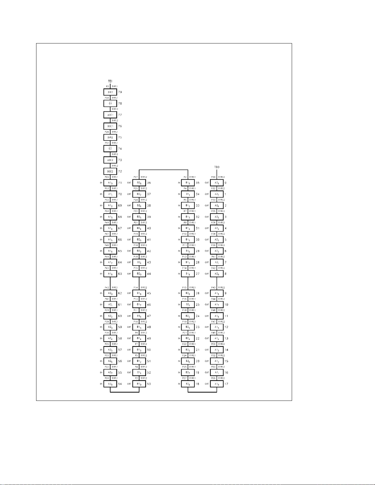
BOUNDARY-SCAN Register
Scan Chain Definition (80 Bits in Length)
http://www.national.com 6
TL/F/11657– 32

Description of BOUNDARY-SCAN Circuitry (Continued)
Input BOUNDARY-SCAN Register
Scan Chain Definition (40 Bits in Length)
When Sample In is Active
TL/F/11657– 33
http://www.national.com7

Description of BOUNDARY-SCAN Circuitry (Continued)
Output BOUNDARY-SCAN Register
Scan Chain Definition (40 Bits in Length)
When Sample Out and EXTEST-Out are Active
http://www.national.com 8
TL/F/11657– 34

Description of BOUNDARY-SCAN Circuitry (Continued)
BOUNDARY-SCAN Register Definition Index
Bit No. Pin Name Pin No. Pin Type Scan Cell Type
79 DIR1 3 Input TYPE1
78 G1
77 AOE
76 BOE
75 DIR2 26 Input TYPE1
1
1
74 G2
73 AOE
72 BOE
71 A1
70 A1
69 A1
68 A1
67 A1
66 A1
65 A1
64 A1
63 A1
62 A2
61 A2
60 A2
59 A2
58 A2
57 A2
56 A2
55 A2
54 A2
53 B1
52 B1
51 B1
50 B1
49 B1
48 B1
47 B1
46 B1
45 B1
44 B2
43 B2
42 B2
41 B2
40 B2
39 B2
38 B2
37 B2
36 B2
35 B1
34 B1
33 B1
32 B1
31 B1
30 B1
29 B1
28 B1
27 B1
2
2
0
1
2
3
4
5
6
7
8
0
1
2
3
4
5
6
7
8
0
1
2
3
4
5
6
7
8
0
1
2
3
4
5
6
7
8
0
1
2
3
4
5
6
7
8
54 Input TYPE1
Internal TYPE2
Internal TYPE2
31 Input TYPE1
Internal TYPE2
Internal TYPE2
55 Input TYPE1
53 Input TYPE1
52 Input TYPE1
50 Input TYPE1
49 Input TYPE1
47 Input TYPE1
46 Input TYPE1
44 Input TYPE1
43 Input TYPE1
42 Input TYPE1
41 Input TYPE1
39 Input TYPE1
38 Input TYPE1
36 Input TYPE1
35 Input TYPE1
33 Input TYPE1
32 Input TYPE1
30 Input TYPE1
2 Output TYPE2
4 Output TYPE2
5 Output TYPE2
7 Output TYPE2
8 Output TYPE2
10 Output TYPE2
11 Output TYPE2
13 Output TYPE2
14 Output TYPE2
15 Output TYPE2
16 Output TYPE2
18 Output TYPE2
19 Output TYPE2
21 Output TYPE2
22 Output TYPE2
24 Output TYPE2
25 Output TYPE2
27 Output TYPE2
2 Input TYPE1
4 Input TYPE1
5 Input TYPE1
7 Input TYPE1
8 Input TYPE1
10 Input TYPE1
11 Input TYPE1
13 Input TYPE1
14 Input TYPE1
Control
Signals
A1–in
A2–in
B1–out
B2–out
B1–in
http://www.national.com9

Description of BOUNDARY-SCAN Circuitry (Continued)
BOUNDARY-SCAN Register Definition Index (Continued)
Bit No. Pin Name Pin No. Pin Type Scan Cell Type
26 B2
25 B2
24 B2
23 B2
22 B2
21 B2
20 B2
19 B2
18 B2
17 A1
16 A1
15 A1
14 A1
13 A1
12 A1
11 A1
10 A1
9A1
8A2
7A2
6A2
5A2
4A2
3A2
2A2
1A2
0A2
0
1
2
3
4
5
6
7
8
0
1
2
3
4
5
6
7
8
0
1
2
3
4
5
6
7
8
15 Input TYPE1
16 Input TYPE1
18 Input TYPE1
19 Input TYPE1
21 Input TYPE1
22 Input TYPE1
24 Input TYPE1
25 Input TYPE1
27 Input TYPE1
55 Output TYPE2
53 Output TYPE2
52 Output TYPE2
50 Output TYPE2
49 Output TYPE2
47 Output TYPE2
46 Output TYPE2
44 Output TYPE2
43 Output TYPE2
42 Output TYPE2
41 Output TYPE2
39 Output TYPE2
38 Output TYPE2
36 Output TYPE2
35 Output TYPE2
33 Output TYPE2
32 Output TYPE2
30 Output TYPE2
B2–in
A1–out
A2–out
http://www.national.com 10

SCAN ABT Live Insertion and Power Cycling Characteristics
SCAN ABT is intended to serve in Live Insertion backplane
applications. It provides 2nd Level Isolation
1
which indicates
that while external circuitry to control the output enable pin
is unnecessary, there may be a need to implement differential length backplane connector pins for V
well, pre-bias circuitry for backplane pins may be necessary
and GND. As
CC
to avoid capacitive loading effects during live insertion.
SCAN ABT provides control of output enable pins during
power cycling via the circuit in
trols the G
During
pin until VCCreaches a known level.
n
power-up
, when VCCramps through the 0.0V to 0.7V
Figure A
. It essentially con-
range, all internal device circuitry is inactive, leaving output
and I/O pins of the device in high impedance. From approximately 0.8V to 1.8V V
(POR), in
Figure A
, the Power-On-Reset circuitry,
CC
becomes active and maintains device
high impedance mode. The POR does this by providing a
low from its output that resets the flip-flop The output, Q
,of
the flip-flop then goes high and disables the NOR gate from
an incidental low input on the G
POR circuitry becomes inactive and ceases to control the
pin. After 1.8V VCC, the
n
flip-flop. To bring the device out of high impedance, the G
input must receive an inactive-to-active transition, a high-tolow transition on G
flip-flop. With a low on the Q
in this case to change the state of the
n
output of the flip-flop, the NOR
gate is free to allow propagation of a G
During
power-down
, the Power-On-Reset circuitry will become active and reset the flip-flop at approximately 1.8V
V
. Again, the Q output of the flip-flop returns to a high and
CC
disables the NOR gate from inputs from the G
device will then remain in high impedance for the remaining
ramp down from 1.8V to 0.0V V
Some suggestions to help the designer with live insertion
issues:
The Gnpin can float during power-up until the Power-On-
#
Reset circuitry becomes inactive.
The Gnpin can float on power-down only after the Pow-
#
er-On-Reset has become active.
The description of the functionality of the Power-On-Reset
circuitry can best be described in the diagram of
CC
n
signal.
n
pin. The
n
.
Figure B
.
FIGURE A
FIGURE B
1
Section 7, ‘‘Design Consideration for Fault Tolerant Backplanes’’, Application Note AN-881.
SCAN ABT includes additional power-on reset circuitry not otherwise included in ABT devices.
TL/F/11657– 19
TL/F/11657– 20
http://www.national.com11

Absolute Maximum Ratings (Note 1)
If Military/Aerospace specified devices are required,
please contact the National Semiconductor Sales
Office/Distributors for availability and specifications.
Storage Temperature
Ambient Temperature under Bias
Junction Temperature under Bias
Ceramic
Plastic
VCCPin Potential to
Ground Pin
Input Voltage (Note 2)
Input Current (Note 2)
b
65§Ctoa150§C
b
55§Ctoa125§C
b
55§Ctoa175§C
b
55§Ctoa150§C
b
0.5V toa7.0V
b
0.5V toa7.0V
b
30 mA toa5.0 mA
Voltage Applied to Any Output
in the Disabled or
Power-Off State
in the HIGH State
b
0.5V toa5.5V
b
0.5V to V
Current Applied to Output
in LOW State (Max) Twice the Rated I
(mA)
OL
DC Electrical Characteristics
Symbol Parameter V
V
IH
V
IL
V
CD
V
OH
V
OL
I
IH
I
BVI
I
BVIT
I
IL
V
ID
a
I
IH
a
I
IL
I
OZH
I
OZL
Note 1: Guaranteed not tested.
Input HIGH Voltage 2.0 V Recognized HIGH Signal
Input LOW Voltage 0.8 V Recognized LOW Signal
Input Clamp Diode Voltage Min
Output HIGH Voltage Min 2.5 V I
Mil Min 2.0 V I
Comm Min 2.0 V I
Output LOW Voltage
Mil Min 0.8 V I
Comm Min 0.8 V I
Input HIGH Current
All Others
Max 5 mAV
Max 5 mAV
TMS, TDI Max 5 mAV
Input HIGH Current
Breakdown Test
Input HIGH Current
Breakdown Test (I/O)
Input LOW Current
All Others
Max 7 mA
Max 100 mA
Max
Max
TMS, TDI Max
Input Leakage Test
I
Output Leakage Current Max 50 mAV
OZH
I
Output Leakage Current Max
OZL
Output Leakage Current Max 50 mAV
Output Leakage Current Max
DC Latchup Source Current
Commercial
Military
Over Voltage Latchup (I/O) 10V
ESD (HBM) Min. 2000V
Note 1: Absolute maximum ratings are values beyond which the device may
be damaged or have its useful life impaired. Functional operation under
these conditions is not implied.
Note 2: Either voltage limit or current limit is sufficient to protect inputs.
Recommended Operating
Conditions
Free Air Ambient Temperature
Military
Commercial
CC
CC
0.0 4.75 V
Supply Voltage
Military
Commercial
Minimum Input Edge Rate (DV/Dt)
Data Input 50 mV/ns
Enable Input 20 mV/ns
Min Typ Max Units Conditions
b
1.2 V I
b
5 mAV
b
5 mAV
b
385 mAV
b
50 mAV
b
50 mAV
b
500 mA
b
300 mA
b
55§Ctoa125§C
b
40§Ctoa85§C
a
4.5V toa5.5V
a
4.5V toa5.5V
eb
18 mA
IN
eb
3mA
OH
eb
24 mA
OH
eb
32 mA
OH
e
12 mA
OL
e
15 mA
OL
e
2.7V (Note 1)
IN
e
V
IN
CC
e
V
IN
CC
e
V
7.0V
IN
e
V
5.5V
IN
e
0.5V (Note 1)
IN
e
0.0V
IN
e
0.0V
IN
e
I
1.9 mA
ID
All Other Pins Grounded
e
2.7V
OUT
e
0.5V
OUT
e
2.7V
OUT
e
0.5V
OUT
http://www.national.com 12
DC Electrical Characteristics (Continued)
Symbol Parameter V
I
OS
I
CEX
I
ZZ
I
CCH
I
CCL
I
CCZ
I
CCT
Output Short-Circuit Current Max
Output HIGH Leakage Current Max 50 mAV
Bus Drainage Test
Power Supply Current Max 250 mAV
Power Supply Current Max 65 mA V
Power Supply Current Max 250 mA TDI, TMSeV
Additional ICC/Input
All Other Inputs Max 2.9 mA V
TDI, TMS inputs Max 3 mA V
I
CCD
Dynamic I
CC
No Load
Max 1.0 mA V
Max 65.8 mA V
Max 1.0 mA TDI, TMSeGND
Max 0.2
Min Typ Max Units Conditions
CC
b
100
0.0 100 mA
AC Electrical Characteristics Normal Operation
Military Commercial
Symbol Parameter
t
t
t
t
t
t
PLH
PHL
PLZ
PHZ
PZL
PZH
Propagation Delay
AtoB,BtoA 1.5 4.4 6.5
Disable Time
Enable Time
*Voltage Range 5.0Vg0.5V
V
*
CC
(V)
5.0
5.0
5.0
eb
T
55§Ctoa125§CT
A
e
C
50 pF C
L
Min Typ Max Min Typ Max
b
275 mA V
mA/ Outputs Open
MHz One Bit Toggling, 50% Duty Cycle
1.0 3.1 5.2
1.5 4.8 8.6
1.5 5.2 8.9
1.5 5.5 9.1
1.5 4.6 8.2
e
0.0V
OUT
e
V
OUT
e
V
5.5V
OUT
All Others GND
e
VCC; TDI, TMSeV
OUT
e
VCC; TDI, TMSeGND
OUT
e
LOW; TDI, TMSeV
OUT
e
LOW; TDI, TMSeGND
OUT
e
V
IN
CC
e
V
IN
CC
eb
40§Ctoa85§C
A
e
50 pF
L
CC
CC
CC
CC
b
2.1V
b
2.1V
Units
ns
ns
ns
http://www.national.com13

AC Electrical Characteristics Scan Test Operation
Military Commercial
V
*
Symbol Parameter
t
t
t
t
t
t
t
t
t
t
t
t
PLH
PHL
PLZ
PHZ
PZL
PZH
PLH
PHL
PLH
PHL
PLH
PHL
Propagation Delay
TCK to TDO 4.2 7.7 12.1
Disable Time
TCK to TDO 3.3 7.4 12.5
Enable Time
TCK to TDO 2.8 6.8 11.5
Propagation Delay 2.8 6.3 10.7
TCK to Data Out 5.0 4.5 8.2 13.0
during Update-DR State
Propagation Delay 3.3 7.2 12.2
TCK to Data Out 5.0 5.0 9.3 14.8
during Update-IR State
Propagation Delay 3.7 8.4 14.0
TCK to Data Out
during Test Logic
CC
(V)
5.0
5.0
5.0
5.0
Reset State
t
t
t
t
t
t
PLZ
PHZ
PLZ
PHZ
PLZ
PHZ
Disable Time 2.8 7.6 13.9
TCK to Data Out 5.0 3.5 8.4 14.5
during Update-DR State
Disable Time 3.6 8.7 15.1
TCK to Data Out 5.0 3.8 9.2 15.9
during Update-IR State
Disable Time 4.0 9.8 17.1
TCK to Data Out
during Test Logic
5.0
Reset State
t
t
t
t
t
t
PZL
PZH
PZL
PZH
PZL
PZH
Enable Time 4.4 9.3 15.5
TCK to Data Out 5.0 3.0 7.5 13.3
during Update-DR State
Enable Time 5.2 10.7 17.4
TCK to Data Out 5.0 3.9 9.0 15.4
during Update-IR State
Enable Time 5.7 12.0 19.8
TCK to Data Out
during Test Logic
5.0
Reset State
*Voltage Range 5.0Vg0.5V
All Propagation Delays involving TCK are measured from the falling edge of TCK.
eb
T
55§Ctoa125§CT
A
e
C
50 pF C
L
Min Typ Max Min Typ Max
eb
40§Ctoa85§C
A
e
50 pF
L
2.9 6.1 10.2
2.1 5.9 10.7
4.6 8.7 13.7
5.7 10.8 17.2
4.2 9.9 16.6
3.0 10.2 17.6
Units
ns
ns
ns
ns
ns
ns
ns
ns
ns
ns
ns
ns
http://www.national.com 14
AC Operating Requirements Scan Test Operation
Military Commercial
Symbol Parameter
V
*
CC
(V)
eb
T
55§Ctoa125§CT
A
e
C
50 pF C
L
Guaranteed Minimum
t
S
t
H
t
S
t
H
t
S
t
H
t
S
t
H
t
S
t
H
t
S
t
H
t
W
f
max
t
PU
t
DN
*Voltage Range 5.0Vg0.5V
All Input Timing Delays involving TCK are measured from the rising edge of TCK.
Note 1: Timing pertains to the TYPE1 BSR and TYPE2 BSR after the buffer (BSR 0 –8, 9 –17, 18 –26, 27 –35, 36 –44, 45– 53, 54– 62, 63– 71).
Note 2: Timing pertains to BSR 74 and 78 only.
Note 3: Timing pertains to BSR 72, 73, 76 and 77 only.
Note 4: Timing pertains to BSR 75 and 79 only.
Setup Time
Data to TCK (Note 1)
Hold Time
Data to TCK (Note 1)
Setup Time, H or L
G1
,G2to TCK (Note 2)
Hold Time, H or L
TCK to G1
,G2(Note 2)
Setup Time, H or L
DIR1, DIR2 to TCK (Note 4)
Hold Time, H or L
TCK to DIR1, DIR2 (Note 4)
Setup Time
Internal OE to TCK (Note 3)
Hold Time, H or L
TCK to Internal OE (Note 3)
Setup Time, H or L
TMS to TCK
Hold Time, H or L
TCK to TMS
Setup Time, H or L
TDI to TCK
Hold Time, H or L
TCK to TDI
Pulse Width TCK H
Maximum TCK
Clock Frequency
Wait Time,
Power Up to TCK
5.0 4.8 ns
5.0 2.5 ns
5.0 4.1 ns
5.0 1.7 ns
5.0 4.2 ns
5.0 2.3 ns
5.0 3.8 ns
5.0 2.3 ns
5.0 8.7 ns
5.0 1.5 ns
5.0 6.7 ns
5.0 5.0 ns
5.0
L 8.5
5.0 50 MHz
5.0 100 ns
Power Down Delay 0.0 100 ms
eb
A
40§Ctoa85§C
e
50 pF
L
10.2
Units
ns
Capacitance
Symbol Parameter Typ Units Conditions, T
C
IN
C
(Note 1) Output Capacitance 13.7 pF V
I/O
Note 1: C
is measured at frequency fe1 MHz, per MIL-STD-883B, Method 3012.
I/O
Input Capacitance 5.9 pF V
e
0.0V (Gn, DIRn)
CC
e
5.0V (An,Bn)
CC
e
25§C
A
http://www.national.com15

Ordering Information
SCAN 18 2245 A SS C X
Serially Controlled Access Network Special Variations
18-Bit Logic
Function Type
Technology Designator
e
T
TTL Input TTL Output CMOS Device
e
C
CMOS Input/Output CMOS Device
e
B
Bipolar TTL Device
e
E
ECL Device
e
A
BiCMOS Device
e
TTL Input/CMOS Output CMOS Device
F
e
X
Tape and Reel
e
Military grade device with
QB
environmental and burn-in
processing.
Temperature Range
e
C
Commercial (b40§Cto
a
85§C)
e
M
Military (b55§Ctoa125§C)
Package Code
e
25 mil Pitch (JEDEC) SSOP
SS
e
F
25 mil Pitch Ceramic Flatpak
http://www.national.com 16
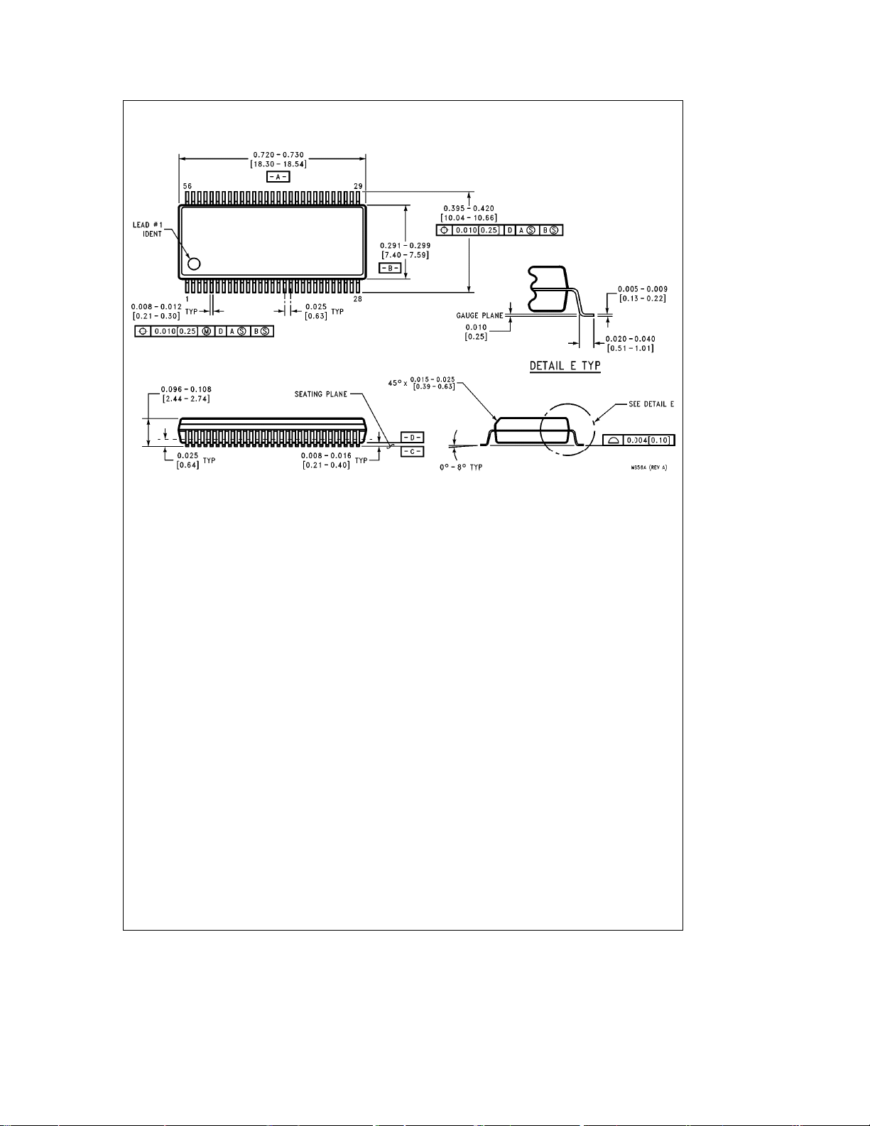
Physical Dimensions inches (millimeters)
Order Number SCAN182245ASSC or SCAN182245ASSCX
56-Lead SSOP (0.300×Wide) (SS)
NS Package Number MS56A
http://www.national.com17

Physical Dimensions inches (millimeters) (Continued)
56-Lead Ceramic Flatpak (F)
Order Number SCAN182245AFMQB
NS Package Number WA56A
SCAN182245A Transceiver with 25X Series Resistor Outputs
LIFE SUPPORT POLICY
NATIONAL’S PRODUCTS ARE NOT AUTHORIZED FOR USE AS CRITICAL COMPONENTS IN LIFE SUPPORT
DEVICES OR SYSTEMS WITHOUT THE EXPRESS WRITTEN APPROVAL OF THE PRESIDENT OF NATIONAL
SEMICONDUCTOR CORPORATION. As used herein:
1. Life support devices or systems are devices or 2. A critical component is any component of a life
systems which, (a) are intended for surgical implant support device or system whose failure to perform can
into the body, or (b) support or sustain life, and whose be reasonably expected to cause the failure of the life
failure to perform, when properly used in accordance support device or system, or to affect its safety or
with instructions for use provided in the labeling, can effectiveness.
be reasonably expected to result in a significant injury
to the user.
National Semiconductor National Semiconductor National Semiconductor National Semiconductor
Corporation Europe Hong Kong Ltd. Japan Ltd.
1111 West Bardin Road Fax:
Arlington, TX 76017 Email: europe.support@nsc.com Ocean Centre, 5 Canton Rd. Fax: 81-043-299-2408
Tel: 1(800) 272-9959 Deutsch Tel:
Fax: 1(800) 737-7018 English Tel:
http://www.national.com
National does not assume any responsibility for use of any circuitry described, no circuit patent licenses are implied and National reserves the right at any time without notice to change said circuitry and specifications.
Fran3ais Tel:
Italiano Tel:a49 (0) 180-534 16 80 Fax: (852) 2736-9960
a
49 (0) 180-530 85 86 13th Floor, Straight Block, Tel: 81-043-299-2308
a
49 (0) 180-530 85 85 Tsimshatsui, Kowloon
a
49 (0) 180-532 78 32 Hong Kong
a
49 (0) 180-532 93 58 Tel: (852) 2737-1600
 Loading...