

December 2003
PC87382
LPC-to-LPC Switch for Docking Stations, with Fast
Infrared Port, Serial Port and GPIOs
PC87382 LPC-to-LPC Switch for Docking Stations, with Fast Infrared Port, Serial Port and GPIOs
Revision 1.2
General Description
ThePC87382,amemberoftheNationalSemiconductorLPC
SuperI/O family, is targeted for a wide range of portable applications.ThePC87382is PC2001 and ACPI compliant, and
features an LPC-to-LPC Switch with hot plugability, Fast Infrared port (FIR, IrDA 1.1compliant), Serial Port, and General-Purpose Input/Output (GPIO) support for a total of eight
ports.
The PC87382 enables glueless implementation of an LPCto-LPC Switch between the motherboard LPC bus and the
Docking Station, and supports hot insertion and hot removal.
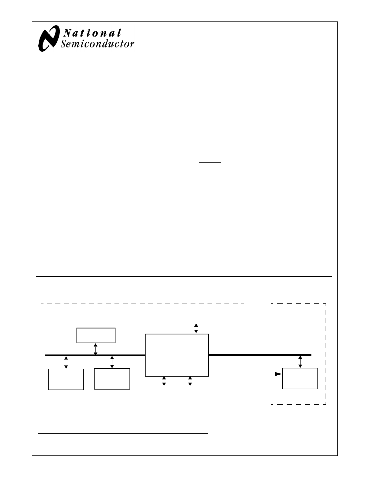
System Block Diagram
Outstanding Features
●
LPC-to-LPC Switch with hot plugability, enables LPC
devices in the Docking Station to be connected to the
Main LPC Bus, thus reducing the number of signals required through the Docking Station connector
●
LPC bus interface, based on Intel’s LPC Interface
Specification Revision 1.1, August 2002 (supports
CLKRUN signal)
●
Fast Infrared port
●
PC2001 and ACPI Revision 2.0 compliant
●
Serial IRQ support (15 options)
●
Protection features, including GPIO lock and pin configuration lock
●
Eight GPIO ports, including with “assert IRQ” capability
●
XOR Tree and TRI-STATEdevice pins (or ICT) testability modes.
●
5V tolerant and back-drive protected pins (except LPC
bus pins)
●
48-pin LQFP package
I/O
Ports
South Bridge
LPC Bus
TPM
National Semiconductor and TRI-STATE are registered trademarks of National Semiconductor Corporation.
All other brand or product names are trademarks or registered trademarks of their respective holders.
©2003 National Semiconductor Corporation
Embedded
Controller
PC87382
Serial
Interface
Infrared
Interface
Portable
Platform
DCLKOUT
Docking
Station
Docking LPC Bus
Docking
SIO
www.national.com
Features
• LPC System Interface
PC87382
— 8-bit I/O cycles
CLKRUN support
—
— Implements PCI mobile design guide recommenda-
tion (PCI Mobile Design Guide 1.1, Dec. 18, 1998)
• LPC-to-LPC Switch
— Hot plugability
CLKRUN support
—
— The connection is controlled by software
— Low switch resistance and propagation delay
— Programmable Clock to Reset Delay
• PC2001 and ACPI Compliant
— PnP Configuration Register structure
— Flexible resource allocation for all logical devices
❏ Relocatable base address
❏ 15 IRQ routing options
❏ Two optional 8-bit DMA channels (where applica-
ble) selected from four possible DMA channels
• Clock Sources
— 14.318 MHz or 48 MHz clock input
— LPC clock, up to 33 MHz
— 14.318 MHz or 48 MHz clock output to the docking
station
• Power Supply
— 3.3V supply operation
— All pins are 5V tolerant, except LPC bus pins
— All pins are back-drive protected, exceptLPC bus pins
• Eight General-Purpose I/O (GPIO) Ports
— Support assert IRQ
— Programmable drive type for each output pin (open-
drain, push-pull or output disable)
— Programmable option for internal pull-up resistor on
each input pin
— Output lock option
— Input debounce mechanism
• Serial Port (SP1)
— Software compatible with the 16550Aandthe 16450
— Shadow register support forwrite-only bit monitoring
— UART data rates up to 1.5 Mbaud
• Fast Infrared Port (FIR)
— Software compatible with the 16550Aandthe 16450
— Shadow register support forwrite-only bit monitoring
— FIR IrDA 1.1 compliant
— HP-SIR
— ASK-IR option of SHARP-IR
— DASK-IR option of SHARP-IR
— Consumer Remote Control supports RC-5, RC-6,
NEC, RCA and RECS 80
— DMA support: 1 or 2 channels
• Strap Configuration
— Base Address (BADDR) straptodetermine the base
address of the Index-Data register pair
— Strap Inputs to select testability mode
• Testability
— XOR Tree
— TRI-STATE device pins
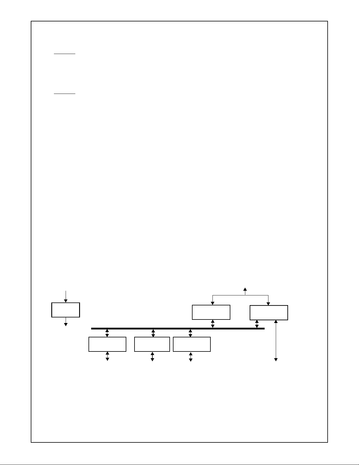
Internal Block Diagram
14.31818 MHz
Clock
Generator
48 MHz
GPIO Ports
Ports
I/O
www.national.com 2 Revision1.2
Serial Port 1
Serial
Interface
FIR
Infrared
Interface
Bus
Interface
LPC Interface
Docking
LPC Switch
Docking LPC
Interface
Revision Record
Revision Date Status Comments
February 2003 Draft 0.1 Specification subject to change without notice.
March 2003 Draft 0.5 Specification subject to change without notice.
March 2003 Preliminary 0.9 Specification subject to change without notice.
April 2003 Preliminary 1.0 Specification subject to change without notice.
November 2003 1.1 Specification subject to change without notice.
December 2003 1.2
●
Added IDDand I
ing edits and typos.
●
Added t
Generator.
●
Technical writing edits and typos.
COR
and t
current numbersTechnical writ-
DDLP
for output from Clock
COF
PC87382
Revision 1.2 3 www.national.com

Table of Contents
PC87382
1.0 Signal/Pin Connection and Description
1.1 CONNECTION DIAGRAM ...........................................................................................................8
1.2 BUFFER TYPES AND SIGNAL/PIN DIRECTORY ......................................................................9
1.3 DETAILED SIGNAL/PIN DESCRIPTIONS ................................................................................10
1.3.1 LPC Bus Interface .......................................................................................................10
1.3.2 Docking LPC Bus ........................................................................................................10
1.3.3 Clocks ..........................................................................................................................10
1.3.4 Infrared (IR) ................................................................................................................11
1.3.5 Serial Port (SP1) ..........................................................................................................11
1.3.6 General-Purpose Input/Output (GPIO) Ports ...............................................................11
1.3.7 Power and Ground .....................................................................................................12
1.3.8 Strap Configuration ......................................................................................................12
1.3.9 Test and Miscellaneous ...............................................................................................12
1.4 INTERNAL PULL-UP AND PULL-DOWN RESISTORS ............................................................13
2.0 Power, Reset and Clocks
2.1 POWER .....................................................................................................................................14
2.1.1 Power Planes ..............................................................................................................14
2.1.2 Power States ...............................................................................................................14
2.1.3 Power Connection and Layout Guidelines ..................................................................14
2.2 RESET SOURCES AND TYPES ...............................................................................................15
2.2.1 VDD Power-Up Reset ..................................................................................................15
2.2.2 Hardware Reset ...........................................................................................................15
2.3 CLOCK DOMAINS .....................................................................................................................15
2.3.1 LPC Domain ................................................................................................................15
2.3.2 48 MHz Domain ...........................................................................................................15
2.3.3 Chip Power-Up ............................................................................................................16
2.3.4 Specifications ..............................................................................................................16
2.4 TESTABILITY SUPPORT ..........................................................................................................16
2.4.1 ICT ...............................................................................................................................16
2.4.2 XOR Tree Testing ........................................................................................................16
2.4.3 Test Mode Entry Sequence .........................................................................................17
3.0 Device Architecture and Configuration
3.1 OVERVIEW ...............................................................................................................................18
3.2 CONFIGURATION STRUCTURE AND ACCESS .....................................................................18
3.2.1 The Index-Data Register Pair ......................................................................................18
3.2.2 Banked Logical Device Registers Structure ................................................................19
3.2.3 Standard Configuration Register Definitions ...............................................................20
3.2.4 Standard Configuration Registers ...............................................................................22
3.2.5 Default Configuration Setup ........................................................................................23
3.3 MODULE CONTROL .................................................................................................................24
3.3.1 Module Enable/Disable ................................................................................................24
www.national.com 4 Revision1.2

Table of Contents (Continued)
3.3.2 Floating Module Output ...............................................................................................24
3.4 INTERNAL ADDRESS DECODING ..........................................................................................25
3.5 PROTECTION ...........................................................................................................................25
3.5.1 Configuration Lock .......................................................................................................25
3.5.2 GPIO Ports Configuration Lock ...................................................................................25
3.5.3 Fast Disable Configuration Lock ..................................................................................25
3.5.4 Clock Control Lock ......................................................................................................25
3.5.5 GPIO Ports Lock ..........................................................................................................25
3.6 REGISTER TYPE ABBREVIATIONS ........................................................................................26
3.7 SUPERI/O CONFIGURATION REGISTERS .............................................................................26
3.7.1 SuperI/O ID Register (SID) ..........................................................................................26
3.7.2 SuperI/O Configuration 1 Register (SIOCF1) ..............................................................27
3.7.3 SuperI/O Configuration 2 Register (SIOCF2) ..............................................................27
3.7.4 SuperI/O Configuration 6 Register (SIOCF6) ..............................................................28
3.7.5 SuperI/O Revision ID Register (SRID) ........................................................................28
3.7.6 Clock Generator Control Register (CLOCKCF) ...........................................................29
3.8 INFRARED CONFIGURATION .................................................................................................30
3.8.1 Logical Device 2 (IR) Configuration .............................................................................30
3.8.2 Infrared Configuration Register ...................................................................................30
PC87382
3.9 SERIAL PORT 1 CONFIGURATION .........................................................................................31
3.9.1 Logical Device 3 (SP1) Configuration ..........................................................................31
3.9.2 Serial Port 1 Configuration Register ............................................................................31
3.10 GENERAL-PURPOSE INPUT/OUTPUT (GPIO) PORTS CONFIGURATION ..........................32
3.10.1 General Description .....................................................................................................32
3.10.2 Implementation ............................................................................................................32
3.10.3 Logical Device 7 (GPIO) Configuration .......................................................................33
3.10.4 GPIO Pin Select Register (GPSEL) .............................................................................34
3.10.5 GPIO Pin Configuration Register (GPCFG) ................................................................34
3.10.6 GPIO Event Routing Register (GPEVR) ......................................................................35
3.11 DOCKING LPC SWITCH CONFIGURATION ............................................................................36
3.11.1 Logical Device 19 (DLPC) Configuration .....................................................................36
4.0 LPC Bus Interface
4.1 OVERVIEW ...............................................................................................................................37
4.2 LPC TRANSACTIONS ...............................................................................................................37
4.3 CLKRUN FUNCTIONALITY ......................................................................................................37
4.4 INTERRUPT SERIALIZER ........................................................................................................37
5.0 General-Purpose Input/Output (GPIO) Port
5.1 OVERVIEW ...............................................................................................................................38
5.2 BASIC FUNCTIONALITY ..........................................................................................................39
5.2.1 Configuration Options ..................................................................................................39
5.2.2 Operation .....................................................................................................................39
Revision 1.2 5 www.national.com

Table of Contents (Continued)
PC87382
5.3 EVENT HANDLING AND SYSTEM NOTIFICATION ................................................................40
5.3.1 Event Configuration .....................................................................................................40
5.3.2 System Notification ......................................................................................................40
5.4 GPIO PORT REGISTERS .........................................................................................................41
5.4.1 GPIO Pin Configuration Registers Structure ...............................................................42
5.4.2 GPIO Port Runtime Register Map ...............................................................................42
5.4.3 GPIO Data Out Register (GPDO) ................................................................................42
5.4.4 GPIO Data In Register (GPDI) ....................................................................................43
5.4.5 GPIO Event Enable Register (GPEVEN) ....................................................................43
5.4.6 GPIO Event Status Register (GPEVST) ......................................................................43
6.0 Docking LPC Switch
6.1 OVERVIEW ...............................................................................................................................44
6.2 FUNCTIONAL DESCRIPTION ..................................................................................................44
6.2.1 Basic Functionality .......................................................................................................44
6.2.2 LDRQ Sharing Mechanism ..........................................................................................44
6.3 DOCKING LPC SWITCH REGISTERS .....................................................................................45
6.3.1 Docking LPC Switch Register Map ..............................................................................45
6.3.2 Docking LPC Control (DLCTL) ....................................................................................45
7.0 Legacy Functional Blocks
7.1 SERIAL PORT 1 (SP1) ..............................................................................................................47
7.1.1 General Description .....................................................................................................47
7.1.2 Register Bank Overview ..............................................................................................47
7.1.3 SP1 Register Maps ......................................................................................................48
7.1.4 SP1 Bitmap Summary .................................................................................................49
7.2 IR FUNCTIONALITY (IR) ...........................................................................................................51
7.2.1 General Description .....................................................................................................51
7.2.2 Register Bank Overview ..............................................................................................51
7.2.3 IR Register Map for IR Functionality ............................................................................52
7.2.4 IR Bitmap Summary for IR Functionality .................................................................55
8.0 Device Characteristics
8.1 GENERAL DC ELECTRICAL CHARACTERISTICS .................................................................58
8.1.1 Recommended Operating Conditions .........................................................................58
8.1.2 Absolute Maximum Ratings .........................................................................................58
8.1.3 Capacitance ................................................................................................................59
8.1.4 Power Consumption under Recommended Operating Conditions ..............................59
8.1.5 Voltage Thresholds ......................................................................................................59
8.2 DC CHARACTERISTICS OF PINS, BY I/O BUFFER TYPES ..................................................59
8.2.1 Input, PCI 3.3V ............................................................................................................59
8.2.2 Input, TTL Compatible .................................................................................................60
8.2.3 Input, TTL Compatible with Schmitt Trigger ................................................................60
8.2.4 Output, PCI 3.3V .........................................................................................................60
www.national.com 6 Revision1.2

Table of Contents (Continued)
8.2.5 Output, Push-Pull Buffer ..............................................................................................60
8.2.6 Output, Open-Drain Buffer ...........................................................................................61
8.2.7 Quick Switch ................................................................................................................61
8.2.8 Exceptions ...................................................................................................................61
8.2.9 Terminology .................................................................................................................61
8.3 INTERNAL RESISTORS ...........................................................................................................62
8.3.1 Pull-Up Resistor ...........................................................................................................62
8.3.2 Pull-Down Resistor ......................................................................................................63
8.4 AC ELECTRICAL CHARACTERISTICS ....................................................................................63
8.4.1 AC Test Conditions ......................................................................................................63
8.4.2 Clock Input Timing .......................................................................................................64
8.4.3 Clock Output Timing ....................................................................................................64
8.4.4 LCLK and LRESET ......................................................................................................65
8.4.5 VDD Power-Up Reset ..................................................................................................66
8.4.6 LPC and SERIRQ Signals ...........................................................................................67
8.4.7 Serial Port, Sharp-IR, SIR and Consumer Remote Control Timing .............................68
8.4.8 MIR and FIR Timing ....................................................................................................69
8.4.9 Modem Control Timing ................................................................................................70
8.4.10 Docking LPC Switch Timing ........................................................................................71
PC87382
Revision 1.2 7 www.national.com
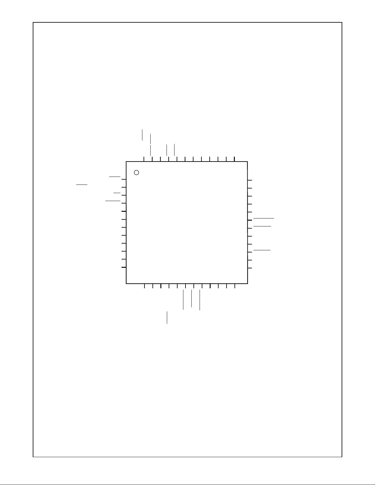
1.0 Signal/Pin Connection and Description
1.1 CONNECTION DIAGRAM
PC87382
/TEST
/TRIS
SOUT1
RTS1
SIN1
DSR1
DCD1
CLKIN
DCLKOUT
LAD3
DLAD3
LAD2
DLAD2
DLAD1
37384044 3941424345464748
CTS1
DTR1_BOUT1/BADDR
RI1
DLDRQ
IRRX1
IRTX
IRRX2_IRSL0
VDD
VSS
VCORF
GPIO00
GPIO01
1
2
3
4
5
6
7
8
9
10
11
12
GPIO02
GPIO03
PC87382
48-Pin LQFP
(Top View)
GPIO04
GPIO20
DLRESET
LDRQ/XOR_OUT
CLKRUN
DCLKRUN
212019181716151413
GPIO21
GPIO23
36
LAD1
35
VDD
34
VSS
33
DLAD0
32
LAD0
31
DLFRAME
30
LFRAME
29
DSERIRQ
28
SERIRQ
LRESET
27
DLCLK
26
LCLK
25
24
2322
VSS
VDD
48-Pin Low Profile Plastic Quad Flatpack (LQFP)
NS Package Number VBH48A
Order Number PC87382-VBH
www.national.com 8 Revision1.2
1.0 Signal/Pin Connection and Description (Continued)
1.2 BUFFER TYPES AND SIGNAL/PIN DIRECTORY
This section describes all signals. Signals are organized in functional groups.
Buffer Types
The signal DC characteristics are denoted by a buffer type symbol, described briefly in Table 1 and in further detail in
Chapter 8 on page 58.
Table 1. Buffer Types
Symbol Description
PC87382
IN
IN
IN
O
O
OD
PCI
T
TS
PCI
p/n
n
Input, PCI 3.3V
Input, TTL compatible
Input, TTL compatible, with Schmidt Trigger
Output, PCI 3.3V
Output, push-pull buffer that is capable of sourcing p mA and sinking n mA
Output, open-drain output buffer that is capable of sinking n mA
QS Quick Switch pin
PWR Power pin
GND Ground pin
Revision 1.2 9 www.national.com
1.0 Signal/Pin Connection and Description (Continued)
1.3 DETAILED SIGNAL/PIN DESCRIPTIONS
PC87382
This section describes all signals of the PC87382.
1.3.1 LPC Bus Interface
Signal Pin(s) I/O Buffer Type Description
LAD3-0 40, 38,
36, 32
LCLK 25 I IN
LDRQ 16 O O
LFRAME 30 I IN
LRESET 27 I IN
SERIRQ 28 I/O IN
CLKRUN 19 I/OD IN
I/O IN
PCI/OPCI
PCI
PCI
PCI
PCI
PCI/OPCI
/OD6Clock Run. Same as PCI CLKRUN.
PCI
LPC Address-Data. Multiplexed command, address bidirectional data
and cycle status.
LPC Clock. Same as PCI clock (up to 33 MHz).
LPC DMA Request. Encoded DMA request for LPC interface.
LPC Frame. Low pulse indicates the beginning of a new LPC cycle or
termination of a broken cycle.
LPC Reset. Same as PCI system reset.
Serial IRQ. The interrupt requests are serialized over a single pin, where
each IRQ level is delivered during a designated time slot.
1.3.2 Docking LPC Bus
Signal Pin(s) I/O Buffer Type Description
DLAD3-0 41, 39,
37, 33
DLCLK 26 I/O QS Dock LPC Clock. Same as PCI clock (up to 33 MHz).
DLFRAME 31 I/O QS Dock LPC Frame. Low pulse indicates the beginning of a new LPC cycle
DSERIRQ 29 I/O QS Dock Serial IRQ. The interrupt requests are serialized over a single pin,
I/O QS Dock LPC Address-Data. Multiplexed command, address bidirectional
data and cycle status.
or termination of a broken cycle.
where each IRQ level is delivered during a designated time slot.
DCLKRUN 20 I/O QS Dock Clock Run. Same as PCI CLKRUN.
DLRESET 18 O O
DLDRQ 4 I IN
4/4
Dock LPC Reset. Main LPC Reset combined with Dock LPC enable.
Dock LPC DMA Request. Encoded DMA request for LPC interface.
T
1.3.3 Clocks
Signal Pin(s) I/O Buffer Type Description
CLKIN 43 I IN
DCLKOUT 42 O O
14/14
Clock In. 14.318 MHz or 48 MHz clock input.
T
Dock Clock Output. Buffered clock for the Docking device. Enabled
together with DLCLK; otherwise in TRI-STATE.
www.national.com 10 Revision1.2
1.0 Signal/Pin Connection and Description (Continued)
1.3.4 Infrared (IR)
Signal Pin(s) I/O Buffer Type Description
PC87382
IRRX1 5 I IN
IRRX2_IRSL0
7 I/O INTS/O
TS
IR Receive 1. Primary input to receive serial data from the IR transceiver.
IRRX2 - IR Receive 2. Auxiliary IR receiver input to support a second
3/6
transceiver.
IRSL0 - IR Select. Output used to control the IR transceiver.
IRTX 6 O O
6/12
IR Transmit. IR serial output data.
1.3.5 Serial Port (SP1)
Signal Pin(s) I/O Buffer Type Description
CTS1 1 I IN
DCD1 44 I IN
DSR1 45 I IN
DTR1_BOUT1 2 O O
RI1 3 I IN
TS
TS
TS
3/6
TS
Clear to Send. When low, indicates that the modem or other data transfer
device is ready to exchange data.
Data Carrier Detected. When low, indicates that the modem or other data
transfer device has detected the data carrier.
Data Set Ready. When low, indicates that the data transfer device, e.g.,
modem, is ready to establish a communications link.
Data Terminal Ready. When low, indicates to the modem or other data
transfer device that the UART is ready to establish a communications link.
Baud Output. Provides the associated serial channel baud rate generator
output signal if Test Mode is selected, i.e., if bit 7 of the EXCR1 register is
set.
Ring Indicator. When low, indicates that a telephone ring signal was
received by the modem. It is monitored during power-off for wake-up event
detection.
RTS1 47 O O
3/6
Request to Send. When low, indicates to the modem or other data
transfer device that the corresponding UART is ready to exchange data. A
system reset sets this signal to inactive high; a loopback operation holds it
inactive.
SIN1 46 I IN
SOUT1 48 O O
TS
3/6
Serial Input. Receives composite serial data from the communications link
(peripheral device, modem or other data transfer device).
Serial Output. Sends composite serial data to the communications link
(peripheral device, modem or other data transfer device). These signals
are set active high after a system reset.
1.3.6 General-Purpose Input/Output (GPIO) Ports
Signal Pin(s) I/O Buffer Type Description
GPIO00-04 11, 12,
13, 14,
15
GPIO20-21,
GPIO23
17, 21
22
I/O IN
OD
I/O IN
OD
/
TS
6,O3/6
/
TS
6,O3/6
General-Purpose I/O Port 0,bits 0-4. Each pin isconfigured independently as inputor I/O, with orwithout static pull-up, andwith either open-drainor
push-pull output type. The port supports interrupt assertion, and each pin
can be enabled or masked as an interrupt source.
General-Purpose I/O Port 2, bits 0,1,3. Same as Port 0, without
interrupt support.
Revision 1.2 11 www.national.com
1.0 Signal/Pin Connection and Description (Continued)
1.3.7 Power and Ground
PC87382
Signal Pin(s) I/O Buffer Type Description
V
DD
V
SS
35, 24, 8 I PWR Main 3.3V Power Supply.
34, 23, 9 I GND Ground.
1.3.8 Strap Configuration
Signal Pin(s) I/O Buffer Type Description
BADDR 2 I IN
TRIS 47 I IN
TEST 48 I IN
TS
TS
TS
Base Address. Sampled at VDDPower-Up reset to determine the base
address of the configuration Index-Data register pair.
– No pull-down resistor (default) - the Index-Data pair at
1
–10KΩ
external pull-down resistor - the Index-Data pair at 2Eh-2Fh1.
The external pull-down resistor must be connected to V
TRI-STATE Device. Sampled at VDDPower-Up to force the device to
float all its output and I/O pins.
– No pull-down resistor (default) - normal pin operation
–10KΩ
1
external pull-down resistor - floating device pins
The external pull-down resistor must be connected to V
TRIS is set to 0 (by an external pull-down resistor), TEST must be
When
1 (i.e., left unconnected).
XOR Tree Test Mode. Sampled at VDDPower-Up to force the device
pins into a XOR tree configuration.
– No pull-down resistor (default) - normal device operation
–10KΩ
1
external pull-down resistor - pins configured as XOR tree.
The external pull-down resistor must be connected to V
TEST is set to 0 (by an external pull-down resistor), TRIS must be
When
1 (i.e., left unconnected).
164Eh-164Fh.
SS
SS
SS
.
.
.
1. Because the strap function is multiplexed with the Serial Port pins, a CMOS transceiver device is recommended
for Serial Port functionality; in this case, the valueof the external pull-down resistor is 10 KΩ. If, however, a TTL
transceiver device is used, the value of the external pull-down resistor must be 470Ω, and since the Serial Port
pins are not able to drive this load, the external pull-down resistor must disconnect t
after VDDpower-up
EPLV
(see Section 8.4.5 on page 66).
1.3.9 Test and Miscellaneous
Signal Pin(s) I/O Buffer Type Description
XOR_OUT 16 O O
3/6
VCORF 10 I/O - On-Chip Core Power Converter Filter. Powers the core logic of all the
www.national.com 12 Revision1.2
XOR Tree Output. All the device pins (except ground and power pins)
are internally connected in a XOR tree structure.
device modules. An external 0.1 µF ceramic filter capacitor must be
connected between this pin and V
SS
.
1.0 Signal/Pin Connection and Description (Continued)
1.4 INTERNAL PULL-UP AND PULL-DOWN RESISTORS
The signals listedin Table 2can optionally support internalpull-up (PU) and/orpull-down (PD) resistors. SeeSection 8.3 on
page 62 for the values of each resistor type.
Table 2. Internal Pull-Up and Pull-Down Resistors
Signal Pin(s) Type Comments
General-Purpose Input/Output (GPIO) Ports
PC87382
GPIO00-04 11, 12,13,
14, 15
GPIO21 21 PU
GPIO20,
17, 22 PU
GPIO23
PU
30
80
30
Programmable
Programmable
Programmable
Strap Configuration and Testability
BADDR 2 PU
TEST 48 PU
TRIS 47 PU
30
30
30
Strap
Strap
Strap
1
1
1
Docking LPC
DLAD3-0 33, 37, 39,
41
DLCLK 26 PU
DCLKOUT 42 PU
DLFRAME 31 PU
DLRESET 18 PD
DSERIRQ 29 PU
DCLKRUN 20 PU
DLDRQ 4 PU
PU
30
30
80
30
120
30
30
30
Active when the switch is off
Active when the switch is off
Active when the switch is off
Active when the switch is off
Active when the switch is off
Active when the switch is off
Active when the switch is off
1. Active only during VDD Power-Up reset.
2. The DockingLPC signal resistors are active when the corresponding
switch is off.
2
2
2
2
2
2
2
Revision 1.2 13 www.national.com
2.0 Power, Reset and Clocks
2.1 POWER
PC87382
2.1.1 Power Planes
The PC87382 has asingle 3.3V power source,VDD. Internally, an additionalpower plane (V
chip voltage converter. This power plane feeds all the core logic.
2.1.2 Power States
The following terminology is used in this document to describe the power states:
) is generated usingan on-
CORF
• Power On - V
• Power Off - V
is active.
DD
is inactive.
DD
2.1.3 Power Connection and Layout Guidelines
The PC87382 requires a power supply voltage of 3.3V ± 10% for the VDDsupply. The on-chip Core voltage converter generates a voltage below 3V for the internal logic.
V
and V
DD
To obtain the best performance, bear in mind the following recommendations.
Ground Connection. The following items must be connected to the ground layer (V
• The ground return (V
• The decoupling capacitors of the Main power supply (V
• The decoupling capacitor of the on-chip Core power converter (V
Note that a low-impedance ground layer also improves noise isolation.
Decoupling Capacitors. The following decoupling capacitors must be used in order to reduce EMI and ground bounce:
• Main power supply (V
dition, place one 10−47 µF tantalum capacitor on the common net as close to the device as possible.
• On-Chip Core power converter (V
pin as possible.
use a common ground return marked VSS.
CORF
) pins
SS
): Place one 0.1 µF capacitor on each VDD-VSSpin pair, as close to the pin as possible. In ad-
DD
): Place one 0.1 µF ceramic capacitor on the V
CORF
DD
) pins
CORF
) pin
) as close to the device as possible:
SS
CORF-VSS
pin pair as close to the
Main 3.3V
8
V
10
DD
V
V
SS
CORF
PC87382
9
µF
+
0.1 µF
0.1 µF
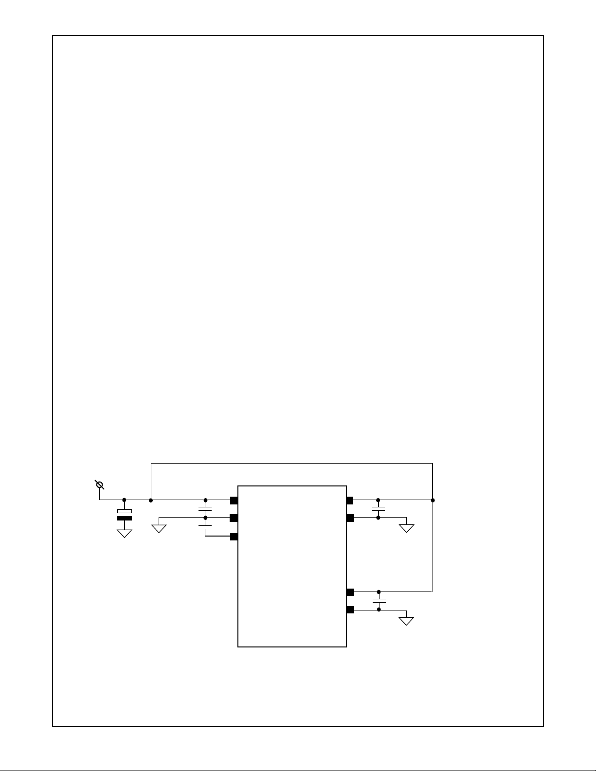
Figure 1. Decoupling Capacitors Connection
10-47
www.national.com 14 Revision1.2
V
V
V
V
DD
SS
DD
SS
24
23
35
34
0.1 µF
0.1 µF
2.0 Power, Reset and Clocks (Continued)
2.2 RESET SOURCES AND TYPES
The PC87382 has the following reset sources:
• V
Power-Up Reset - activated when VDDis powered up
DD
• Hardware Reset - activated when the LRESET input is asserted (low)
2.2.1 VDD Power-Up Reset
VDDPower-Up reset is generated byan internal circuit when VDDpower is turned on. VDDPower-Up reset time (t
until the
that the PC87382 operates correctly.
External devices must waitat least t
this time, the PC87382 LPC interface ignores the transaction (that is, it does not return a SYNC handshake).
V
LRESET signal is de-asserted. The Hardware reset (LRESET)must be asserted for aminimum of 10 ms to ensure
before accessing the PC87382.If the host processoraccesses the PC87382 during
IRST
Power-Up reset performs the following actions:
DD
IRST
) lasts
• Puts pins with strap options into TRI-STATE and enables their internal pull-up resistors
• Samples the logic levels of the strap pins
• Executes all the actions performed by the Hardware reset; see Section 2.2.2
2.2.2 Hardware Reset
Hardware reset is activatedbyassertion of LRESET inputwhileVDDis “good”. When VDDpower is off, thePC87382ignores
the level of the
LRESET input. Hardware reset performs the following actions:
PC87382
• Resets all lock bits in configuration registers
• Loads default values to all the bits in the Configuration Control
• Resets all the logical devices
• Loads default values to all the module registers
2.3 CLOCK DOMAINS
The PC87382 has two clock domains, as shown in Table 3.
Table 3. Clock Domains of the PC87382
Clock
Domain
LPC Up to 33 MHz LPC clock input (LCLK)
48 MHz 48 MHz
2.3.1 LPC Domain
The LPC clock signal at theLCLKpinmustbecome valid before the end of theHardwarereset(LRESET); see Section 2.2.2.
This clock can be slowed down or stopped using the
2.3.2 48 MHz Domain
The 48 MHz clock domain is sourced either by the on-chip Clock Generator or directly by the CLKIN input pin. The Clock
Generator is fed by applying a clock source at a frequency of 14.31818 MHz. The Clock Generator generates two internal
clocks, 24 MHz and 48 MHz. After power-up or Hardware reset, the clock (Clock Generator or external clock) is disabled.
Frequency Source Usage
LPC bus interface and Configuration registers,
On-chip Clock Generator or
directly from Clock Input (CLKIN)
CLKRUN protocol.
Docking LPC Switch logic
Legacy functions (Serial Port, Infrared)
and DCLKOUT output pin
Clock Generator Functional Description
The on-chip Clock Generator starts working when it is enabled by bit 7 of the CLOCKCF register, Index 29h, i.e., when the
bit value changes from 0 to 1 (only for 14.31818 MHz clock source). Once enabled, the output clock is frozen to a steady
logic level until theclockgenerator provides a stableoutputclock that meets all requirements.Then the clock starts toggling.
On Hardware reset, the chip wakes up with the on-chip Clock Generator disabled. The input clock of the Clock Generator
may toggle regardless of the state of the
Revision 1.2 15 www.national.com
LRESET pin. The Clock Generator waits for a toggling input clock.
2.0 Power, Reset and Clocks (Continued)
Bit 4 (read only) of the CLOCKCF register is the Valid Clock Generator status bit. While stabilizing, the output clock is frozen
PC87382
to a steady logic level,andthe status bit is clearedto0to indicate a frozen clock.Whenthe clock generator is stable,theoutput
clock starts togglingand the status bit is set to 1. The status bit tells the software when the ClockGenerator is ready.The software should poll this status bit until itis set (1), and only then activate theUART, the Infraredinterface and the DCLKOUT pin.
The clock generator and its output clock do not consume power when they are disabled.
2.3.3 Chip Power-Up
To ensure proper operation, proceed as follows after power-up:
1. Set bits 5 and 6 of the Clock Generator Control register (CLOCKCF) at Index 29h according to the clock source used
and the desired output frequency on DCLKOUT; see Table 4.
2. Enable the clock. If the clock source is 14.31818 MHz:
— Poll bit 4 of the CLOCKCF register while the clock generator is stabilizing.
— When bit 4 of CLOCKCF is set to 1, go to step 3.
3. Enable any module in the chip, as needed.
Table 4. Clock Generator Encoding Options
CLKIN Pin Frequency Desired DCLKOUT Frequency CLOCKCF Bits 6, 5
48 MHz 48 MHz 00
14.31818 MHz 14.31818 MHz 01
48 MHz 11
2.3.4 Specifications
Wake-uptime is 33 msec (maximum). This is measured from thetime theClockGeneratorisenableduntiltheclockis stable.
Note: The reference clock must be stable at the time the Clock Generator is enabled. Tolerance (long term deviation) of
the generator output clock, relative to the input clock, is ±110 ppm. Total tolerance is therefore
± (input clock tolerance + 110 ppm).
2.4 TESTABILITY SUPPORT
The PC87382 supports two testability modes:
• In-Circuit Testing (ICT)
• XOR Tree Testing
2.4.1 ICT
The In-Circuit Testing (ICT) technique, also known as “bed-of-nails”, injects logic patterns to the input pins of the devices
mounted on the tested board. It then checks their outputs for the correct logic levels.
The PC87382 supports this testing technique by floating (putting in TRI-STATE) all the device pins. This prevents “backdriving” the PC87382pins by the ICT tester when adevice normally controlledby PC87382 is tested(device inputs aredriven by the ICT tester).
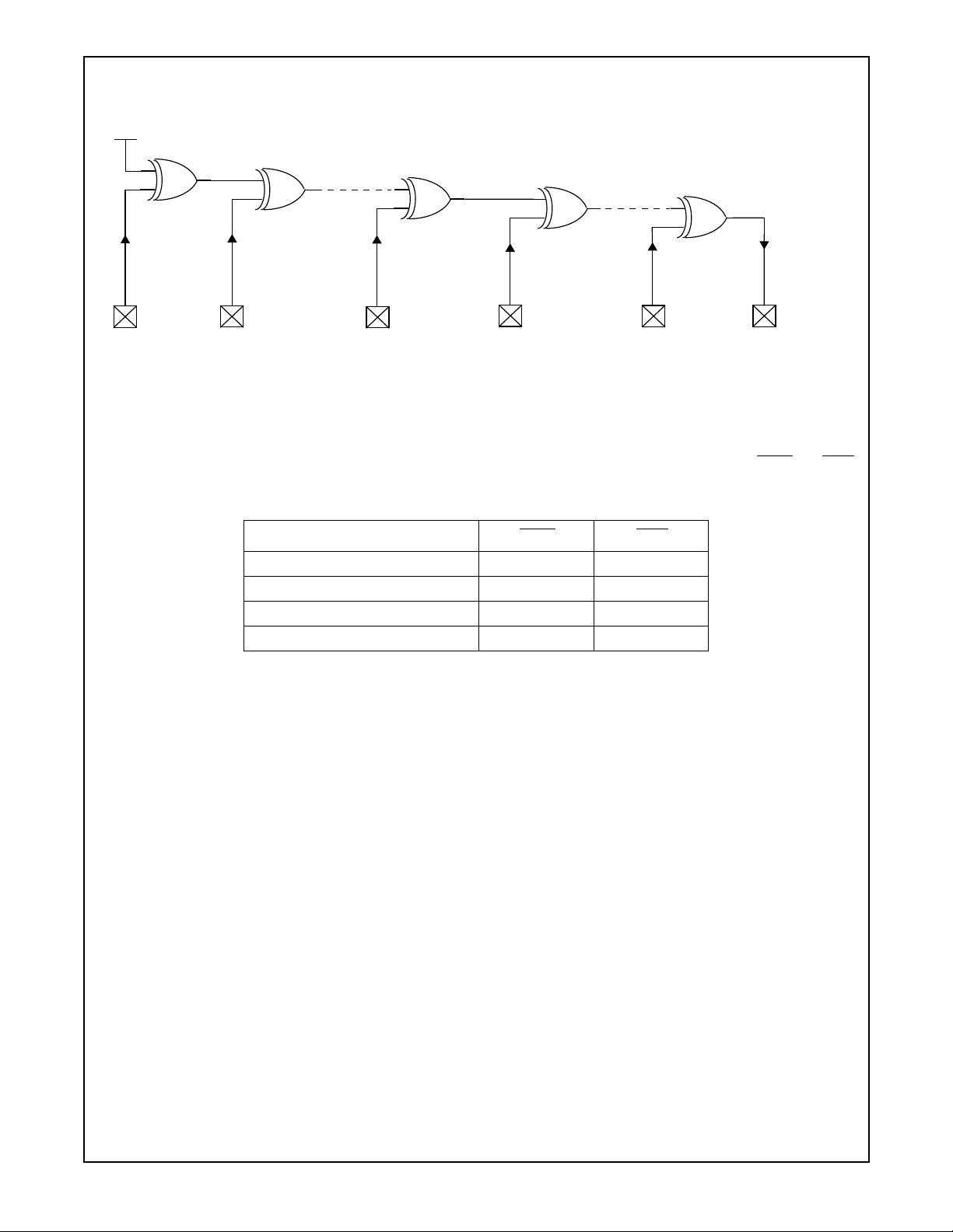
2.4.2 XOR Tree Testing
When the PC87382 ismounted on aboard, it can betested using the XORTree technique. This testalso checks the correct
connection of the device pins to the board.
In XOR Tree mode,all PC87382 pins areconfigured as inputs, exceptthe last pin inthe tree, which istheXOR_OUT output. The
buffer type of theinput pins participating intheXOR tree is IN
in normal device operation mode (see Section 1.3 on page 10). The input pins are chained through XOR gates, as shown in
Figure 2. The power and ground pins (VDD, VSS, VCORF) are excluded from the XOR tree.
(Input, TTL compatible), regardlessof the buffer typeof these pins
T
www.national.com 16 Revision1.2
2.0 Power, Reset and Clocks (Continued)
V
DD
XOR_OUT
Pin 17 Pin 18 Pin 48 Pin 1 Pin 15 Pin 16
Figure 2. XOR Tree (Simplified Diagram)
The maximum propagation delay through the XOR tree, from the first pin in the chain to XOR_OUT is 200 ns.
2.4.3 Test Mode Entry Sequence
Table 5 shows thedecoding values required toentereach test mode. Thetest modes are decodedfrom the TEST andTRIS
strap pins and are latched into PC87382 on power up.
Table 5. Test Mode Selection
PC87382
Test Mode
No Test Mode Selected 1 1
ICT 1 0
XOR Tree 0 1
Reserved exclusively for NSC use 0 0
TEST TRIS
Revision 1.2 17 www.national.com
3.0 Device Architecture and Configuration
The PC87382 comprises a collectionoflegacy and proprietary functional blocks. Eachfunctionalblock is described in aseparate chapter. This chapter describes the PC87382 structure and provides all logical device specific information, including
PC87382
special implementation of generic blocks, system interface and device configuration.
3.1 OVERVIEW
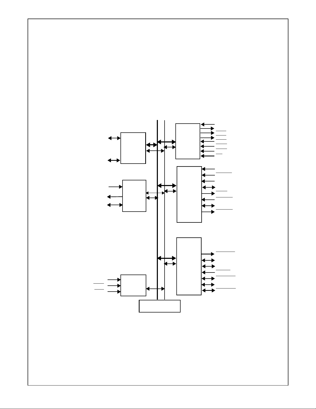
The PC87382 consists of fourlogical devices, the host interface, and a central set of configuration registers, allbuilt around
a central internal bus. Figure 3 illustrates the blocks and related logic.
The system interface serves as a bridge between the external LPC interfaceand the internal bus. It supports 8-bitread and
write transactions for I/O and DMA, as defined in Intel’s LPC Interface Specification, Revision 1.1.
The central configuration register set is ACPI compliant and supports a PnP configuration. The configuration registers are
structured as a subset ofthePlugand Play Standard registers, definedinAppendix A of the Plug andPlayISA Specification,
Revision 1.0a by Inteland Microsoft. Allsystem resources assigned to the functional blocks(I/O address space,DMA channels and IRQ lines) are configured in, and managed by, the central configuration register set. In addition, some functionspecific parameters are configurable throughthe configuration registers and distributedtothe functional blocks throughspecial control signals.
SIN1
SOUT1
RTS1
GPIO20,21,23
GPIO00-04
IRRX1,IRRX2
IRTX
IRSL0
GPIO
Ports
IR
Serial
Port 1
Bus
Interface
DTR1_BOUT1
CTS1
DSR1
DCD1
RI1
CLKIN
LRESET
LCLK
SERIRQ
LDRQ
LFRAME
LAD3-0
CLKRUN
Internal Bus
Control Signals
DLRESET
DLCLK
DSERIRQ
DLDRQ
DLFRAME
DLAD3-0
DCLKRUN
BADDR
TEST
TRIS
LPC
Bus
Switch
Strap
Config
Config &
Control Registers
Figure 3. PC87382 Detailed Block Diagram
3.2 CONFIGURATION STRUCTURE AND ACCESS
The configuration structure is comprised of a set of banked registerswhich are accessed via a pair of specialized registers.
3.2.1 The Index-Data Register Pair
Access to the PC87382 configuration registers is via an Index-Data register pair, using only two system I/O byte locations.
Thebase address of this register pair is determined during V
ping option on the BADDR pin. Table 6 shows the selected base addresses as a function of BADDR.
Power-Upreset, according to the state of the hardware strap-
DD
www.national.com 18 Revision1.2
3.0 Device Architecture and Configuration (Continued)
Table 6. BADDR Strapping Options
I/O Address
BADDR
Index Register Data Register
0 2Eh 2Fh
1 (default) 164Eh 164Fh
The Index registeris an 8-bit read/write register located at the selected baseaddress (Base+0). Itis used asa pointer to the
configuration register file, and holds the index of the configuration register that is currently accessible via the Data register.
Reading the Index register returns the last value written to it (or the default of 00h after reset).
The Data register isan 8-bit register(Base+1) used as adata path to anyconfiguration register. Accessing theData register
actually accesses the configuration register that is currently pointed to by the Index register.
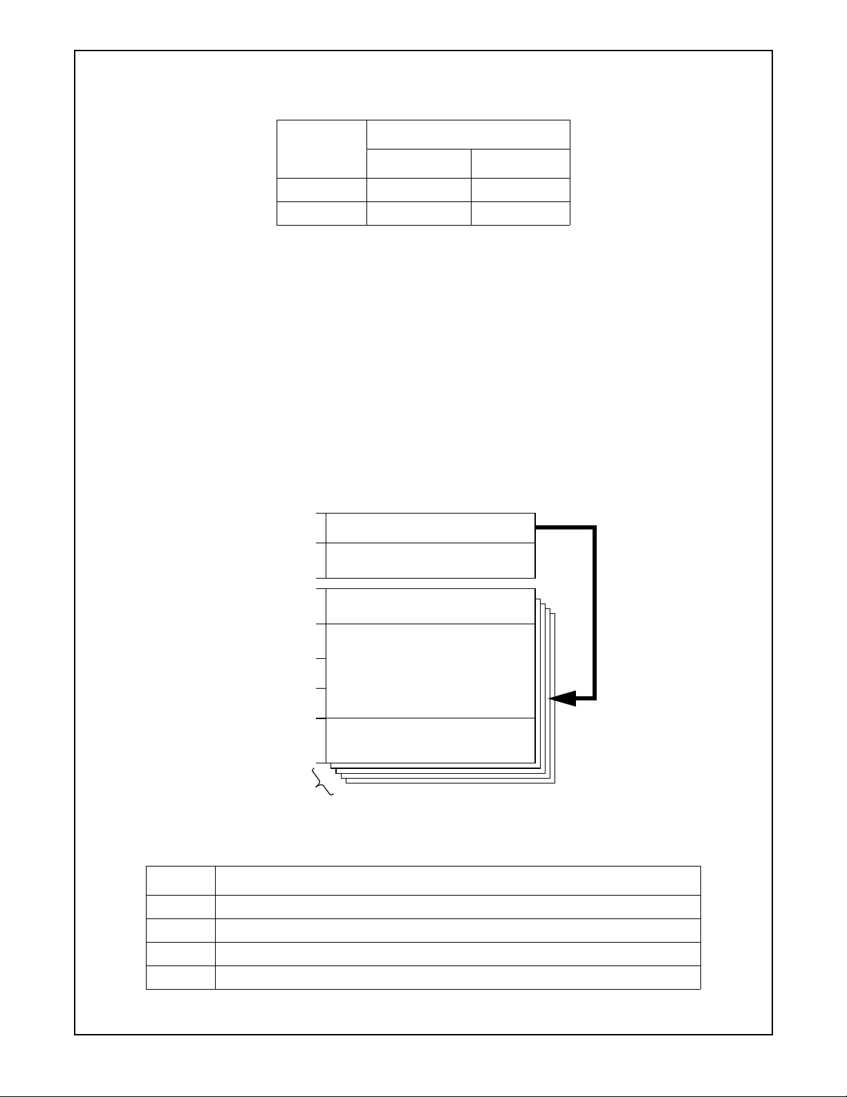
3.2.2 Banked Logical Device Registers Structure
Eachfunctional block is associated with a Logical Device Number (LDN).Theconfigurationregistersaregroupedintobanks,
where each bank holdsthe standard configuration registersofthe corresponding logical device.Table 7 showsthe LDN values of the PC87382 functional blocks. Any value not listed is reserved.
Figure 4 shows the structure of the standard configuration register file. The LDN and PC87382 configuration registers are
notbanked and are accessed by the Index-Data register pair only, as described in Section 3.2.1. However, the device control
and device configuration registers are duplicated over four banks for four logical devices. Therefore, accessing a specific
register in a specific bank is performed by two-dimensional indexing, where the LDN register selects the bank (or logical
device) and the Indexregister selects the registerwithin the bank. Accessingthe Data register whilethe Index register holds
a value of 30h or higher physically accesses the logical device configuration registers currently pointed to by the Index register, within the logical device currently selected by the LDN register.
PC87382
07h
Logical Device Number Register
20h
SuperI/O Configuration Registers
2Fh
Logical Device Control Register
30h
60h
63h
70h
71h
74h
75h
F0h
FFh
Banks
(One per Logical Device)
Figure 4. Structure of Standard Configuration Register File
Table 7. Logical Device Number (LDN) Assignments
LDN Functional Block
02h Infrared (IR)
Standard Logical Device
Configuration Registers
Special (Vendor-defined)
Logical Device
Configuration Registers
Bank Select
03h Serial Port 1 (SP1)
07h General-Purpose I/O (GPIO) Ports
19h Docking LPC Switch
Revision 1.2 19 www.national.com

3.0 Device Architecture and Configuration (Continued)
Write accesses to unimplemented registers(i.e., accessing the Data registerwhilethe Index register points toanon-existing
PC87382
register) are ignored; reads return 00h on all addresses, except 74h and 75h (DMA configuration registers), which return
04h (indicating no DMA channel is active). The configuration registers are accessible immediately after reset.
3.2.3 Standard Configuration Register Definitions
In the registers below, any undefined bit is reserved. Unless otherwise noted, the following definitions also hold true:
●
All registers are read/write.
●
All reserved bits return 0 on reads, except where noted otherwise. To prevent unpredictable results, do not modify
these bits. Use read-modify-write to prevent the values of reserved bits from being changed during write.
●
Write-only registers must not use read-modify-write during updates.
Table 8. Standard General Configuration Registers
Index Register Name Description
07h Logical Device
Number
20h-2Fh PC87382
This register selects the current logical device. See Table 7 for valid numbers. All
other values are reserved.
PC87382 configuration registers and ID registers.
Configuration
Table 9. Logical Device Activate Register
Index Register Name Description
30h Activate Bits 7-1: Reserved.
Bit 0: Logical device activation control; see Section 3.3 on page 24.
0: Disabled
1: Enabled
Table 10. I/O Space Configuration Registers
Index Register Name Description
60h I/O Port Base
Indicates selected I/O lower limit address bits 15−8 for I/O Descriptor 0.
Address Bits 15−8
Descriptor 0
61h I/O Port Base
Indicates selected I/O lower limit address bits 7−0 for I/O Descriptor 0.
Address Bits 7−0
Descriptor 0
www.national.com 20 Revision1.2

3.0 Device Architecture and Configuration (Continued)
Table 11. Interrupt Configuration Registers
Index Register Name Description
70h Interrupt Number Indicates selected interrupt number.
Bits 7-4: Reserved.
Bits 3-0: These bits select the interrupt number. A value of 1 selects IRQ1. A value
of 15 selects IRQ15. IRQ0 is not a valid interrupt selection and
represents no interrupt selection.
Note: Avoid selecting the same interrupt number (except 0) for different logical
devices, as it causes the PC87382 to behave unpredictably.
PC87382
71h Interrupt Request
Type Select
Index Register Name Description
74h DMA Channel
Select 0
Indicates the type and polarity of the interrupt request number selected in the
previous register. If a logical device supports only one type of interrupt, the
corresponding bit is read only.
Bits 7-2: Reserved.
Bit 1: Polarity of interrupt request selected in previous register.
0: Low polarity.
1: High polarity.
Bit 0: Type of interrupt request selected in previous register.
0: Edge.
1: Level.
Table 12. DMA Configuration Registers
Indicates selected DMA channel for DMA 0 of the logical device (0 is the first DMA
channel if more than one DMA channel is used).
Bits 7-3: Reserved.
Bits 2-0: These select the DMA channel for DMA 0, where:
- A value of 0, 1, 2, or 3 selects DMA channel 0, 1, 2, or 3, respectively.
- A value of 4 indicates that no DMA channel is active.
- The values 5-7 are reserved.
Note: Avoid selecting the same DMA channel (except 4) for different logical
devices, as it causes the PC87382 to behave unpredictably.
75h DMA Channel
Select 1
Index Register Name Description
F0h-FFh Logical Device
Configuration
Revision 1.2 21 www.national.com
Indicates selected DMA channel for DMA 1 of the logical device (1 is the second
DMA channel if more than one DMA channel is used).
Bits 7-3: Reserved.
Bits 2-0: These select the DMA channel for DMA 1, where:
- A value of 0, 1, 2, or 3 selects DMA channel 0, 1, 2, or 3, respectively.
- A value of 4 indicates that no DMA channel is active.
- The values 5−7 are reserved.
Note: Avoid selecting the same DMA channel (except 4) for different logical
devices, as it causes the PC87382 to behave unpredictably.
Table 13. Special Logical Device Configuration Registers
Special (vendor-defined) configuration options.
3.0 Device Architecture and Configuration (Continued)
3.2.4 Standard Configuration Registers
PC87382
Index Register Name
07h Logical Device Number
20h SuperI/O ID
21h SuperI/O Configuration 1
22h SuperI/O Configuration 2
SuperI/O Control and
Configuration Registers
Logical Device Control and
Configuration Registers -
one per Logical Device
(some are optional)
23h-25h Reserved
26h SuperI/O Configuration 6
27h SuperI/O Revision ID
28h Reserved
29h Clock Generator Control
2Ah - 2Fh Reserved exclusively for National use
30h Logical Device Control (Activate)
60h I/O Base Address Descriptor 0 Bits 15-8
61h I/O Base Address Descriptor 0 Bits 7-0
70h Interrupt Number and Wake-Up on IRQ Enable
71h IRQ Type Select
74h DMA Channel Select 0
75h DMA Channel Select 1
F0h - FFh Device Specific Logical Device Configuration 1 to 15
Figure 5. Configuration Register Map
SuperI/O Configuration Registers
The PC87382 configuration registers at Indexes 20h and 27h are used for part identification. The other configuration
registers are used for global power management and the selection of pin multiplexing options. For details, see Section 3.7
on page 26.
Logical Device Control and Configuration Registers
A subset of theseregisters is implemented for eachlogical device. See thefunctionalblock descriptions in thefollowing sections.
Control
The only implemented control register for each logical device is the Activate register at Index 30h. Bit 0 of the Activate register controls the activation of the associated functional block. Activation enables access to the functional block’s registers,
and attaches its system resources, which are unassigned aslongasitisnotactivated. Other effects may apply on a functionspecific basis (such as clock enable and activepinout signaling). Access to the configuration register ofthe logical deviceis
enabled even when the logical device is not activated.
Standard Configuration
The standard configuration registers manage the PnPresourceallocationtothe functional blocks. The I/O portbaseaddress
descriptor 0 is a pair of registers at Index 60-61h, holding the first 16-bit base address for the register set of the functional
block. An optional 16-bit second base-address (descriptor 1) at Index 62-63h isused for logical devices withmore than one
continuous register set. Interrupt Number (Index 70h)and IRQ Type Select(Index 71h) allocatean IRQ line tothe block and
control its type. DMA Channel Select 0 (Index 74h) allocates a DMA channel to the block, where applicable. DMA Channel
Select 1 (Index 75h) allocates a second DMA channel, where applicable.
www.national.com 22 Revision1.2

3.0 Device Architecture and Configuration (Continued)
Special Configuration
The vendor-defined registers, starting at Index F0h, control function-specific parameters such as operation modes, power
saving modes, pin TRI-STATE, and non-standard extensions to generic functions.
3.2.5 Default Configuration Setup
In the event of a VDD Power-Up or Hardware reset, the PC87382 wakes up with the following default configuration setup:
— The configuration base address is 2Eh or 164Eh, according to the BADDR strap pin value, as shown in Table 6 on
page 19.
— All logical devices are disabled.
— All multiplexed GPIO pins are configured to their respective default function. When configured as GPIO, they have
an internal static pull-up (default direction is input).
— The legacy devices (Serial Port and IR) are assigned with their legacy system resource allocation.
— National Semiconductor proprietary functions are not assigned with any default resources, and the default values of
their base addresses are all 00h.
See Section 2.2 on page 15 for more details on PC87382 reset sources and types.
PC87382
Revision 1.2 23 www.national.com

3.0 Device Architecture and Configuration (Continued)
3.3 MODULE CONTROL
PC87382
3.3.1 Module Enable/Disable
Module control is performed primarily through the Activation bit (bit 0 of Index 30h) of each logical device. The operation of
each module can be controlled by the host through the LPC bus.
Module enable/disable by the host through the LPC bus is controlled by the following bits:
●
Activation bit (bit 0) in Index 30h of the Standard configuration registers; see Section 3.2.3 on page 20.
●
Fast Disable bit in SIOCF6 register; for the Serial Port 1 and IR modules only; see Section3.7.4 on page 28.
●
Global Enable bit (GLOBEN) in SIOCF1 register; see Section 3.7.2 on page 27.
A module is enabled only if all of these bits are set to their “enable” value.
When a legacy (SP1 or IR) module is disabled, the following takes place:
●
The host system resources of the logical device (IRQ, DMA and runtime address range) are unassigned.
●
Access to the standard- and device-specific Logical De vice configuration registers through the LPC bus remains enabled.
●
Access to the module’s runtime registers through the LPC bus is disabled (transactions are ignored; SYNC cycle is
not generated).
●
The module’s internal clock is disabled (the module is not functional) to lower the power consumption.
When the GPIO or DLPC module is disabled, the following takes place:
●
The host system resources of the logical device (IRQ and runtime address range) are unassigned.
●
Access to the standard- and device-specific Logical De vice configuration registers through the LPC bus remains enabled.
●
Access to the module’s runtime registers through the LPC bus is disabled (transactions are ignored; SYNC cycle is
not generated).
●
The module is functional.
3.3.2 Floating Module Output
The pins of the Legacy modules (Serial Port, Infrared) can be floated. When the TRI-STATE Control bit (bit 0) is set in the
specific module configurationregister (at Index F0hof the specificlogical device in the configuration space) andthe module
is disabled (see Section 3.3.1), the module output signals are floated and the I/O signalsare configured as inputs (notethat
the logic level at the inputs is ignored by the module, which is disabled).
Figure 6 shows the control mechanism for floating the pins of a Legacy module.
Device Configuration
Index 30h
Register
SIOCF1
Register
SIOCF6
Register
Legacy Module
Configuration
Register
(Index F0h)
Activation
Bit (bit 0)
Global
Enable
GLOBEN
Fast
Disable
xxxDIS
TRI-
STATE
Control
Module Enable
Legacy
Module
1
Enable
Output
Buffer
1. Wherever the bit is implemented
Figure 6. Control of Floating Legacy Module Pins
www.national.com 24 Revision1.2

3.0 Device Architecture and Configuration (Continued)
3.4 INTERNAL ADDRESS DECODING
A full 16-bit address decodingisappliedwhen accessing the configuration I/Ospaceas well as the registersofthefunctional
blocks. However, the number of configurable bits in the base address registers varies for each logical device.
The lower 1,2, 3, 4 or5 address bits aredecoded within thefunctional block to determinethe offset of theaccessed register
within the logical device’s I/O range of 2, 4, 8, 16 or 32 bytes, respectively. The remaining bits are matched with the base
address register to decode the entire I/O range allocated to the logical device. Therefore the lower bits of the base address
register are forced to 0 (read only), andthe base address is forcedto be 2, 4, 8, 16 or 32byte-aligned, according to the size
of the I/O range.
The base addresses of the Serial Port 1 and FIR modules are limited to the I/O address range of 00h to 7FXh only (bits1115 are forced to 0). The addressesof the non-legacy logicaldevices are configurablewithin the full 16-bitaddress range (up
to FFFXh).
3.5 PROTECTION
The PC87382 provides features to protect the hardware configuration from changes made by application software running
on the host.
The protection is activated by the software setting a “sticky” lock bit. Each lock bit protects a group of configuration bits located either in the same register or in different registers. When the lock bit is set, the lock bit and all the protected bits become read only and cannot be further modified by the host through the LPC bus. All the lock bits are reset by Hardware
reset, thus unlocking the protected configuration bits.
The bit locking protection mechanism is optional.
The protected groups of configuration bits are described below.
PC87382
3.5.1 Configuration Lock
Lock bit: LOCKMCF in SIOCF1 register (Device Configuration).
Protected bits: LOCKMCF and IOWAIT (in SIOCF1 register) and all bits in SIOCF2 register (Device Configuration).
3.5.2 GPIO Ports Configuration Lock
Protects the configuration (but not the data) of all the GPIO Ports.
Lock bit: LOCKGCF in SIOCF1 register (Device Configuration).
Protected bits for each GPIO Port: LOCKGCF in SIOCF1 register, and all bits in GPCFG register (except LOCKCFP bit) and
GPEVR register (Device Configuration).
3.5.3 Fast Disable Configuration Lock
Protects the Fast Disable bits for all the Legacy modules.
Lock bit: LOCKFDS in SIOCF6 register (Device Configuration).
Protected bits: All bits in SIOCF6 register (except General-Purpose Scratch bits) and GLOBEN bit in SIOCF1 register
(Device Configuration).
3.5.4 Clock Control Lock
Protects the Clock Generator control bits.
Lock bit: LOCKCCF in CLOCKCF register (Device Configuration).
Protected bits: All bits in CLOCKCF register (Device Configuration).
3.5.5 GPIO Ports Lock
Protects the configuration and data of all the GPIO Ports.
Lock bit: LOCKCFP in GPCFG register, for each GPIO Port (Device Configuration).
Protected bits for each GPIO Port: PUPCTL, OUTTYPE and OUTENA in GPCFG register; the corresponding bit (to the
port pin) in GPDO register (GPIO Ports).
Revision 1.2 25 www.national.com

3.0 Device Architecture and Configuration (Continued)
3.6 REGISTER TYPE ABBREVIATIONS
PC87382
The following abbreviations are used to indicate the Register Type:
●
R/W = Read/Write.
●
R = Read from a specific address returns the value of a specific register. Write to the same address is to a dif-
●
W = Write.
●
RO = Read Only.
●
R/W1C = Read/Write 1 to Clear. Writing 1 to a bit clears it to 0. Writing 0 has no effect.
●
R/W1S = Read/Write 1 to Set. Writing 1 to a bit sets its value to 1. Writing 0 has no effect.
3.7 SUPERI/O CONFIGURATION REGISTERS
This section describes the SuperI/O configuration and ID registers (those registers with first level indexes in the range of
20h-2Eh). See Table 14 for a summary and directory of these registers.
Note: Set the configuration registers to enable functions or signals that are relevant to the specific device. The values of
23h-25h Reserved for National use
2Ah - 2Fh Reserved exclusively for National use
ferent register.
fields that select functions, or signals, that are excluded from a specific device are treated as reserved and should
not be selected.
Table 14. SuperI/O Configuration Registers
Index Mnemonic Register Name Type Section
20h SID SuperI/O ID RO 3.7.1
21h SIOCF1 SuperI/O Configuration 1 R/W 3.7.2
22h SIOCF2 SuperI/O Configuration 2 R/W 3.7.3
26h SIOCF6 SuperI/O Configuration 6 R/W 3.7.4
27h SRID SuperI/O Revision ID RO 3.7.5
29h CLOCKCF Clock Generator Control Register R/W 3.7.6
3.7.1 SuperI/O ID Register (SID)
This register contains the identity number of the chip. The PC87382 family is identified by the value F4h.
Location: Index 20h
Type: RO
Bit 76543210
Name
Reset F4h
www.national.com 26 Revision1.2
Chip ID

3.0 Device Architecture and Configuration (Continued)
3.7.2 SuperI/O Configuration 1 Register (SIOCF1)
Location: Index 21h
Type: Varies per bit
Bit 76543210
Name LOCKMCF LOCKGCF Reserved IOWAIT Reserved GLOBEN
Reset 0 0 0 10001
Bit Type Description
PC87382
7 R/W1S LOCKMCF (Lock Multiplexing Configuration). When set to 1, this bit locks the configuration of
6 R/W1S LOCKGCF (Lock GPIO Pins Configuration). When set to 1, this bit locks the configuration registers
5-4 Reserved. These bits must be ‘01’.
3-2 R/W orROIOWAIT (Number of I/O Wait States). These bits set the number of wait states for I/O transactions
1 Reserved. This bit must be 0.
0 R/W orROGLOBEN (Global Device Enable). This bit makes it possible to disable all logical devices by setting a
registers SIOCF1 and SIOCF2 by disabling writing to all bits in these registers (including the LOCKMCF
bit itself), except for the LOCKGCF and GLOBEN bits in SIOCF1. Once set, this bit can only be cleared
by Hardware reset.
0: R/W bits are enabled for write (default).
1: All bits are RO.
of all GPIO pins (see Section 3.10.3 on page 33) by disabling writes to all their bits (including the
LOCKGCF bit itself). The locked registers include the GPCFG (except LOCKCFP bit) and GPEVR
registers of all GPIO pins. Once set, this bit can only be cleared by Hardware reset.
0: R/W bits are enabled for write (default).
1: All bits are RO.
through the LPC bus.
Bits
3 2 Number of Wait States
0 0: 0 (default)
0 1: 2
1 0: 6
1 1: 12
single bit (to 0). In addition, when the bit is set to 1, it enables the operation of all the logical devices
of the PC87382, as long as the logical device is itself enabled (see Table 7 on page 19). The behavior
of the different devices is explained in Section3.3 on page 24.
0: All logical devices in the PC87382 are disabled and their resources are released.
1: Enables each PC87382 logical device that is itself enabled (default); see Section 3.3.1 on page 24.
3.7.3 SuperI/O Configuration 2 Register (SIOCF2)
This register is reset by hardware to 63h.
Location: Index 22h
Type: R/W or RO
This register is reserved. It must be written with 63h
Revision 1.2 27 www.national.com

3.0 Device Architecture and Configuration (Continued)
3.7.4 SuperI/O Configuration 6 Register (SIOCF6)
PC87382
This register providesa fast wayto disable oneor more moduleswithout having toaccess the Activateregister of each;see
Section 3.3.1 on page 24.
Location: Index 26h
Type: Varies per bit
Bit 76543210
Name
Reset 00000000
Bit Type Description
7 R/W1SLOCKFDS (Lock Fast Disable Configuration). When set to 1, this bit locks itself, SER1DIS and IRDIS
6-5 R/W General-Purpose Scratch.
4 Reserved.
3 R/W
2 R/W
1-0 Reserved.
or RO
or RO
LOCKFDS
bits in this register and GLOBEN bit in SIOCF1 register by disabling writing to all of these bits. Once set,
this bit can only be cleared by Hardware reset.
0: R/W bits are enabled for write (default).
1: All bits are RO.
SER1DIS (Serial Port 1 Disable).
0: Enabled or Disabled, according to Activation bit (default).
1: Disabled.
IRDIS (Infrared Disable).
0: Enabled or Disabled, according to Activation bit (default).
1: Disabled.
General-Purpose
Scratch
Reserved SER1DIS IRDIS Reserved
3.7.5 SuperI/O Revision ID Register (SRID)
This register contains the ID number of the specific family member (Chip ID) and the chip revision number (Chip Rev).
Location: Index 27h
Type: RO
Bit 76543210
Name
Reset 0 0 0 XXXXX
Bit Description
7-5 Chip ID.
4-0 Chip Rev. These bits identify the device revision.
Chip ID Chip Rev
www.national.com 28 Revision1.2

3.0 Device Architecture and Configuration (Continued)
3.7.6 Clock Generator Control Register (CLOCKCF)
Location: Index 29h
Type: Varies per bit
Bit 76543210
Name CKEN CKOUTSEL CK48SEL CKVALID LOCKCCF Reserved
Reset 0 0 0 00000
Bit Type Description
PC87382
7 R/W orROCKEN (Clock Enable). This bit enables the internal clock of the PC87382. If the clock source selected
6 R/W orROCKOUTSEL (Clock Output Select). Selects the clock source to output on DCLKOUT pin.
5 R/W orROCK48SEL (48 MHz Clock Select). Selects the source of the internal 48 MHz clock.
4ROCKVALID (Valid Clock Generator, Clock Status). This bit indicates the status of the on-chip, 48 MHz
3 R/W1S LOCKCCF (Lock Clock Configuration). When set to 1, this bit locks the CLOCKCF register by
by CK48SEL bit is the Clock Generator, CKEN enables the Clock Generator; otherwise it enables the
path from the CLKIN input pin.
0: Clock disabled (default).
1: Clock enabled.
0: Select Clock Source from CLKIN pin (default).
1: Select Clock Generator Output. Valid only if CK48SEL field is set.
0: The source of the internal 48 MHz clock is CLKIN pin (default).
Use when CLKIN pin is connected to a 48 MHz clock source.
1: The source of the internal 48 MHz clock is the Clock Generator.
Use when CLKIN pin is connected to a 14.31818 MHz clock source.
Clock Generator and controls the generator output clock signal. The PC87382 modules using this clock
may be enabled (see Section 3.3.1 on page 24) only after this bit is read high (generator clock is valid).
0: Generator output clock frozen (default).
1: Generator output clock active (stable and toggling).
disabling writing to all its bits (including to the LOCKCCF bit itself). Once set, this bit can only be
cleared by Hardware reset.
0: The R/W bits are enabled for write (default).
1: All the bits are Read-Only.
2-0 Reserved.
Revision 1.2 29 www.national.com

3.0 Device Architecture and Configuration (Continued)
3.8 INFRARED CONFIGURATION
PC87382
3.8.1 Logical Device 2 (IR) Configuration
Table 15lists the configurationregisters that affect the Infrared. Only the last register (F0h) isdescribed here. SeeSections
3.2.3 and 3.2.4 for descriptions of the other registers.
Table 15. Infrared Configuration Registers
Index Configuration Register or Action Type Reset
30h Activate. See also bit 0 of the SIOCF1 register and bit 2 of the SIOCF6 register. R/W 00h
60h Base Address MSB register. Bits 7-3 (for A15-11) are read only, 00000b. R/W 02h
61h Base Address LSB register. Bit 2-0 (for A2-0) are read only, 000b. R/W F8h
70h Interrupt Number and Wake-Up on IRQ Enable register. R/W 03h
71h Interrupt Type. Bit 1 is R/W; other bits are read only. R/W 03h
74h DMA Channel Select 0 (RX_DMA). R/W 04h
75h DMA Channel Select 1 (TX_DMA). R/W 04h
F0h Infrared Configuration register. R/W 02h
3.8.2 Infrared Configuration Register
This register is reset by hardware to 02h.
Location: Index F0h
Type: R/W
Bit 76543210
Name Bank
Reset 00000010
Bit Description
7 Bank Select Enable. Enables bank switching for Infrared.
0: All attempts to access the extended registers in Infrared are ignored (default).
1: Enables bank switching for Infrared.
6-3 Reserved.
2 Busy Indicator. This read-only bit can be used by power management software to decide when to power down
the Infrared logical device.
0: No transfer in progress (default).
1: Transfer in progress.
1 Power Mode Control. When the logical device is active in:
0: Low power mode
1: Normal power mode
0 TRI-STATE Control. When enabled and the device is inactive, the logical device output pins are in TRI-STATE.
One exception is the IRTX pin, which is driven to 0 when Infrared is inactive and is not affected by this bit.
0: TRI-STATE disabled (default).
1: TRI-STATE enabled.
Select
Enable
Infrared clock disabled. The output signals are set to their default states. Registers are maintained (unlike
Active bit in Index 30, which also prevents access to Infrared registers).
Infrared clock enabled. Infrared is functional when the logical device is active (default).
Reserved
Busy
Indicator
Power
Mode
Control
TRI-STATE
Control
www.national.com 30 Revision1.2

3.0 Device Architecture and Configuration (Continued)
3.9 SERIAL PORT 1 CONFIGURATION
3.9.1 Logical Device 3 (SP1) Configuration
Table 16lists the configuration registersthat affect the SerialPort 1. Onlythe last register (F0h)is described here. See Sections 3.2.3 and 3.2.4 for descriptions of the other registers.
Table 16. Serial Port 1 Configuration Registers
Index Configuration Register or Action Type Reset
30h Activate. See also bit 0 of the SIOCF1 register and bit 3 of the SIOCF6 register. R/W 00h
60h Base Address MSB register. Bits 7-3 (for A15-11) are read only, 00000b. R/W 03h
61h Base Address LSB register. Bit 2-0 (for A2-0) are read only, 000b. R/W F8h
70h Interrupt Number and Wake-Up on IRQ Enable register. R/W 04h
71h Interrupt Type. Bit 1 is R/W; other bits are read only. R/W 03h
74h Report no DMA Assignment. RO 04h
75h Report no DMA Assignment. RO 04h
F0h Serial Port 1 Configuration register. R/W 02h
PC87382
3.9.2 Serial Port 1 Configuration Register
This register is reset by hardware to 02h.
Location: Index F0h
Type: R/W
Bit 76543210
Name Bank
Reset 00000010
Bit Description
7 Bank Select Enable. Enables bank switching for Serial Port 1.
0: Disabled (default).
1: Enabled.
6-3 Reserved.
2 Busy Indicator. This read-only bit can be used by power management software to decide when to power down
the Serial Port 1 logical device.
0: No transfer in progress (default).
1: Transfer in progress.
1 Power Mode Control. When the logical device is active in:
0: Low power mode
1: Normal power mode
Select
Enable
Serial Port 1 clock disabled. The output signals are set to their default states. The
programmed to generate an interrupt. Register values are maintained (unlike Active bit in Index 30, which also
prevents access to Serial Port 1 registers).
Serial Port 1 clock enabled. Serial Port 1 is functional when the logical device is active (default).
Reserved
Busy
Indicator
Power
Mode
Control
RI input signal can be
TRI-STATE
Control
0 TRI-STATE Control. When enabled and the device is inactive, the logical device output pins are in TRI-STATE.
0: Disabled (default).
1: Enabled.
Revision 1.2 31 www.national.com

3.0 Device Architecture and Configuration (Continued)
3.10 GENERAL-PURPOSE INPUT/OUTPUT (GPIO) PORTS CONFIGURATION
PC87382
3.10.1 General Description
The GPIO functional block includes eight pins arranged in two 8-bit ports:
●
Port 0 contains five GPIOE pins (i.e., GPIO pins with event detection).
●
Port 2 contains three GPIO pins (i.e., GPIO pins without event detection).
All pins in port 0 have full event detection capability, enabling them to trigger the assertion of IRQ signals. Pins in port 2 do
not have event detection capability. The runtime registers associated with the two ports are arranged in the GPIO address
space as shown in Table 17. The GPIO base address is 16-byte aligned. Address bits 3-0 are used to indicate the register
offset.
Table 17. Runtime Registers in GPIO Address Space
Offset Mnemonic Register Name Port Type
00h GPDO0 GPIO Data Out 0 0 R/W
01h GPDI0 GPIO Data In 0 RO
02h GPEVEN0 GPIO Event Enable 0 R/W
03h GPEVST0 GPIO Event Status 0 R/W1C
04h-07h Reserved
08h GPDO2 Data Out 2 2 R/W
09h GPDI2 Data In 2 RO
3.10.2 Implementation
The standard GPIO port with event detection capability (such as port 0) has four runtime registers. Each pin is associated
with a GPIO Pin Configuration register that includes seven configuration bits. Port 2 is a non-standard port that does not
support event detection, and therefore differs from the generic model as follows:
●
It has two runtime registers for basic functionality: GPDO2 and GPDI2. Event detection registers GPEVEN2 and
GPEVST2 are not available.
●
Only bits 3-0 are implemented in the GPIO Pin Configuration register of port 2. Bits 6-4, associated with the event
detection functionality, are reserved.
www.national.com 32 Revision1.2

3.0 Device Architecture and Configuration (Continued)
3.10.3 Logical Device 7 (GPIO) Configuration
Table 18 lists the configuration registers that affect the GPIO. Only the last three registers (F0h - F2h) are described here.
See Sections 3.2.3 and 3.2.4 for a detailed description of the other registers.
Table 18. GPIO Configuration Register
Index Configuration Register or Action Type Reset
30h Activate. See also bit 7 of the SIOCF1 register. R/W 00h
60h Base Address MSB register. R/W 00h
61h Base Address LSB register. Bits 3-0 (for A3-0) are read only, 0000b. R/W 00h
70h Interrupt Number register. R/W 00h
71h Interrupt Type. Bit 1 is read/write. Other bits are read only. R/W 03h
74h Report no DMA assignment. RO 04h
75h Report no DMA assignment. RO 04h
F0h GPIO Pin Select register (GPSEL). R/W 00h
F1h GPIO Pin Configuration register (GPCFG). Varies per bit
F2h GPIO Pin Event Routing register (GPEVR). R/W or RO 01h
04h or 44h
PC87382
1
1. Depending on port number
Figure 7 shows the organization of these registers.
GPIO Pin Select Register
(Index F0h)
Port Select
Port 0
GPIO Pin
Configuration Register
(Index F1h)
Port 2
Pin Select
Pin 0
Pin 7
Pin 0
Port 2, Pin 0
Port 0, Pin 0
Configuration Registers
Port 0, Pin 7
Port 0, Pin 0
GPIO Pin Event
Routing Register
(Index F2h)
Pin 7
Figure 7. Organization of GPIO Pin Registers
Revision 1.2 33 www.national.com
Event Routing
Registers
Port 0, Pin 7

3.0 Device Architecture and Configuration (Continued)
3.10.4 GPIO Pin Select Register (GPSEL)
PC87382
This register selects the GPIO pin (port number and bit number) to be configured (i.e., which register is accessed via the
GPIO Pin Configuration register). It is reset by hardware to 00h.
Location: Index F0h
Type: R/W
Bit 76543210
Name Reserved PORTSEL Reserved PINSEL
Reset 00000000
Bit Description
7-6 Reserved.
5-4 PORTSEL (Port Select). These bits select the GPIO port to be configured:
Bits
5 4 GPIO Port
0 0: Port 0 (default)
0 1: Reserved
1 0: Port 2
1 1: Reserved
3 Reserved.
2-0 PINSEL (Pin Select). These bits select the GPIO pin to be configured in the selected port:
000, 001,... 111: Binary value of the pin number, 0, 1,... 7 respectively (default=0).
For port 2 only values 000,001,011 are legal.
3.10.5 GPIO Pin Configuration Register (GPCFG)
This register reflects, for both read and write, the register currently selected by the GPIO Pin Select register (GPSEL). All
the GPIO Pin registers that are accessed via this register have a common bit structure, as shown below. This register is
reset by hardware to 44h for port 0, and to 04h for port 2.
Location: Index F1h
Type: Varies per bit
Port 0, bits 0-4 (with event detection capability)
Bit 76543210
Name Reserved EVDBNC EVPOL EVTYPE LOCKCFP PUPCTL OUTTYPE OUTENA
Reset 01000100
Port 2, bits 0,1,3 (without event detection capability)
Bit 76543210
Name Reserved LOCKCFP PUPCTL OUTTYPE OUTENA
Reset 00000100
Bit Type Description
7 Reserved.
6 R/W orROEVDBNC (Event Debounce Enable). (Ports 0 and 1 with event detection capability). Enables
www.national.com 34 Revision1.2
transferring the signal only after a predetermined debounce period.
0: Disabled.
1: Enabled (default).
Reserved. (Port 2). Always 0.

3.0 Device Architecture and Configuration (Continued)
Bit Type Description
PC87382
5 R/W orROEVPOL (Event Polarity). (Ports 0 and 1 with event detection capability). This bit defines the polarity of
4 R/W orROEVTYPE (Event Type). (Ports 0 and 1 with event detection capability). This bit defines the type of the
3 R/W1S LOCKCFP (Lock Configuration of Pin). When set to 1, this bit locks the GPIO pin configuration and
2 R/W orROPUPCTL (Pull-Up Control). This bit is used to enable/disable the internal pull-up capability of the
1 R/W or
the signal that issues an interrupt from the corresponding GPIO pin (falling/low or rising/high).
0: Falling edge or low level input (default).
1: Rising edge or high level input.
Reserved. (Port 2). Always 0.
signal that issues an interrupt from the corresponding GPIO pin (edge or level).
0: Edge input (default).
1: Level input.
Reserved. (Port 2). Always 0.
data (see also Section 5.4 on page 41) by disabling writing to itself, to GPCFG register bits PUPCTL,
OUTTYPE and OUTENA, and to the corresponding bit in GPDO register. Once set, this bit can only be
cleared by Hardware reset.
0: R/W bits are enabled for write (default).
1: All bits are RO.
corresponding GPIO pin. It supports open-drain output signals with internal pull-ups and TTL input
signals.
0: Disabled.
1: Enabled (default).
OUTTYPE(Output Type). This bit controls the output buffer type (open-drain or push-pull) of the
RO
corresponding GPIO pin.
0: Open-drain (default).
1: Push-pull.
0 R/W orROOUTENA (Output Enable). This bit indicates the GPIO pin output state. It has no effect on the input
path.
0: TRI-STATE (default).
1: Output enabled.
3.10.6 GPIO Event Routing Register (GPEVR)
This register enables the routing of the GPIO event to IRQ signals. It is implemented only for ports 0,1 which have event
detection capability. This register is reset by hardware to 00h.
Location: Index F2h
Type: R/W
Bit 76543210
Name Reserved EV2IRQ
Reset 00000000
Bit Description
7-1 Reserved.
0 EV2IRQ (Event to IRQ Routing). Controls the routing of the event from the selected GPIO pin to IRQ; see
Section 5.3.2 on page 40.
0: Disabled (default).
1: Enabled.
Revision 1.2 35 www.national.com

3.0 Device Architecture and Configuration (Continued)
3.11 DOCKING LPC SWITCH CONFIGURATION
PC87382
3.11.1 Logical Device 19 (DLPC) Configuration
Table 19lists the configuration registers that affect theDLPC. See Sections 3.2.3 and 3.2.4 for descriptions of the registers
summarized below.
Table 19. DLPC Configuration Registers
Index Configuration Register or Action Type Reset
30h Activate. See also bit 0 of the SIOCF1 register. R/W 00h
60h Base Address MSB register. R/W 00h
61h Base Address LSB register. Bit 0 (for A0) is read only, 0b. R/W 00h
70h Interrupt Number register. No Interrupt assignment. RO 00h
71h Interrupt Type. No Interrupt assignment. RO 00h
74h Report no DMA assignment. RO 04h
75h Report no DMA assignment. RO 04h
www.national.com 36 Revision1.2

4.0 LPC Bus Interface
4.1 OVERVIEW
The LPC host Interface supports 8-bit I/O Read and Write and 8-bit DMA transactions, as defined in Intel’s LPC Interface
Specification, Revision 1.1.
4.2 LPC TRANSACTIONS
The LPC Interface of the PC87382 can respond to the following LPC transactions:
●
8-bit I/O read and write cycles
●
8-bit DMA read and write cycles
●
DMA request cycles
4.3 CLKRUN FUNCTIONALITY
The PC87382 supports the CLKRUN signal, which is implemented according to the specification in PCI Mobile Design
Guide, Revision 1.1, December 18, 1998. The PC87382supportsoperationwithbotha slow and stopped clock in ACPI state
S0 (when the system is active but is not being accessed). In the following cases, the PC87382 drives the
low to force the LPC bus clock into full speed operation:
●
An IRQ is pending internally, waiting to be sent through the serial IRQ.
●
A DMA request is pending internally, waiting to be sent through the serial DMA.
Note: When the
CLKRUN signal is not in use, the PC87382 assumes a valid clock on the LCLK pin.
CLKRUN signal
PC87382
4.4 INTERRUPT SERIALIZER
The Interrupt Serializer translates parallel interrupt request signals received from internal IRQ sources, into serial interrupt
request data transmitted over the SERIRQ bus.
The internal IRQs arefed into a Mapping,Enable and PolarityControl block, which mapsthem to their associatedIRQ slots.
The IRQs are then fed into the Interrupt Serializer, where they are translated into serial data and transmitted over the SERIRQ bus.
The same slot cannot be shared among different interrupt sources in the device.
Revision 1.2 37 www.national.com

5.0 General-Purpose Input/Output (GPIO) Port
This chapter describes one 8-bit port. A device may include a combination of several ports with different implementations.
For the device specific implementation, see Section 3.10 on page 32.
PC87382
5.1 OVERVIEW
The GPIO port is an 8-bit port, which is based on eight pins. It features:
●
Software capability to manipulate and read pin levels
●
Controllable system notification by several means based on the pin level or level transition
●
Ability to capture and manipulate events and their associated status
●
Back-drive protected pins.
GPIO port operation is associated with two sets of registers:
●
Pin Configuration registers, mapped in the Device Configuration space. These registers are used to set up the logical
behavior of each pin. There are two 8-bit registers for each GPIO pin.
●
Four 8-bit runtime registers: GPIO Data Out (GPDO), GPIO Data In (GPDI), GPIO Event Enable (GPEVEN) and
GPIO Event Status (GPEVST). These registers are mapped in the GPIO device I/O space (which is determined by
the base address registers in the GPIO Device Configuration). They are used to manipulate and/or read the pin val-
ues, and to control and handle system notification. Each runtime register corresponds to the 8-pin port, such that bit
n in each one of the four registers is associated with GPIOXn pin, where X is the port number.
Each GPIO pin is associated with ten configuration bits and the corresponding bit slice of the four runtime registers, as
shown in Figure 8.
The functionality of the GPIO port isdividedintobasic functionality, which includes the manipulation andreadingoftheGPIO
pins, and enhanced functionality. Basic functionality is described in Section 5.2. Enhanced functionality, which includes
event detection and system notification, is described in Section 5.3.
X = port number
n = pin number, 0 to 7
GPIO Pin
Configuration (GPCFG)
Register
GPIO Pin
Select (GPSEL)
Register
GPIO Pin Event
Routing (GPEVR)
Register
Port and Pin
Select
GPIOX Base Address
8 GPCFG
Registers
GPIOXn CNFG
8 GPEVR
Registers
GPIOXn ROUTE
Event
Pending
Indicator
Bit n
GPIOXn
Port Logic
x8
GPDOX
GPDIX
GPEVENX
GPEVSTX
x8
Event
Routing
Control
Runtime
Registers
GPIOXn
Pin
x8
Interrupt
Request
Figure 8. GPIO Port Architecture
www.national.com 38 Revision1.2

5.0 General-Purpose Input/Output (GPIO) Port (Continued)
5.2 BASIC FUNCTIONALITY
The basic functionality of each GPIO pin is based on four configuration bits and a bit slice of runtime registers GPDO and
GPDI. The configuration and operation of a single GPIOXn pin (pin n in port X) is shown in Figure 9.
GPIO Device
Enable
PC87382
Internal
Bus
Read Only
Read/Write
Data In
Push-Pull =1
Data Out
Lock
Bit 3 Bit 2 Bit 1 Bit 0
GPIO Pin Configuration (GPCFG) Register
Pull-Up
Control
Output
Type
Static
Pull-Up
Pin
Pull-Up
Enable
Output
Enable
Figure 9. GPIO Basic Functionality
5.2.1 Configuration Options
The GPCFG register controls the following basic configuration options:
• Port Direction - Controlled by the Output Enable bit (bit 0).
• Output Type - Push-pull vs. open-drain. It is controlled by Output Buffer Type (bit 1) by enabling/disabling the pull-up
portion of the output buffer.
• Weak Static Pull-Up - Maybeadded to any type ofport(input, open-drain or push-pull).Itis controlled by Pull-Up Control
(bit 2).
• Pin Lock - GPIO pin may be locked to prevent any changes in the output value and/or the output characteristics. The
lock is controlled by Lock (bit 3). It disables writes to the GPDO register bits, and to bits 0-3 of the GPCFG register (In-
cluding the Lock bit itself). Once locked, it can be released by Hardware reset only.
5.2.2 Operation
The value that is written to the GPDO register is driven to the pin if the output is enabled. Reading from the GPDO register
returns its contents, regardless of the pin value or the port configuration.The GPDI register is aread-only register. Reading
from the GPDI register returns the pin value, regardless of what is driving it (the port itself, configured as an output port, or
the external device when the port is configured as an input port). Writing to this register is ignored.
Activation of the GPIO port is controlled by an external device-specific configurationbit (or a combination ofbits). When the
port is inactive, access to GPDI and GPDO registers is disabled. However, there isno change in the port configuration and
in the GPDO value, and hence there is no effect on the outputs of the pins.
Revision 1.2 39 www.national.com

5.0 General-Purpose Input/Output (GPIO) Port (Continued)
5.3 EVENT HANDLING AND SYSTEM NOTIFICATION
PC87382
The enhanced GPIO port supports system notification based on event detection. This functionality is based on six configuration bits and abit slice of runtimeregisters GPEVEN and GPEVST.The configuration and operationofthe event detection
capability is shown in Figure 10. System notification is shown in Figure 11.
GPIO
Event
Pending
Indication
Pin
Input
Debouncer
0
1
Rising Edge or
High Level =1
Rising
Edge
Detector
1
0
Level =1
GPIO
Status
Set
Reset
Write 1 to Clear
Read
Internal
Bus
R/W
Event
Enable
Event
Debounce
Enable
Bit 6 Bit 5 Bit 4
Event Polarity
Event Type
Figure 10. Event Detection
GPIO Pin Configuration Register
(GPCFG)
5.3.1 Event Configuration
Each pin in the GPIO port is a potential input event source. The event detection can trigger a system notification on predetermined behavior of the source pin. The GPCFG register determines the event detection trigger type for the system notification.
Event Type and Polarity
Two trigger types of event detectionaresupported:edge and level. An edge eventcanbe detected on a source pintransition
either from high to low or low to high. A level event may be detected when the source pin is at active level. The trigger type
is determined by Event Type (bit 4 of the GPCFG register). The direction of the transition (for edge) or the polarity of the
active level (for level) is determined by Event Polarity (bit 5 of the GPCFG register).
Active edge refers to a change in a GPIO pin level that matches the Event Polarity bit (1 for rising edge and 0 for falling
edge). Active level refers to the GPIO pin level that matches the Event Polarity bit (1 for high level and 0 for low level). The
corresponding bit inGPEVST register isset by hardwarewhenever an activeedge or anactive level isdetected, regardless
of the GPEVEN register setting. Writing 1 to the Status bit clears it to 0. Writing 0 is ignored.
Event Debounce Enable
The input signal can be debounced for at least 16 msec before enteringthe Rising Edge detector. The signal state is transferred to the detector only after a debouncing period during which the signal has no transitions, to ensure that the signal is
stable. The debouncer adds 16 msec delay to both assertion and de-assertion of the event pending indicator. Therefore,
when working with a level event and system notification by IRQ, it is recommended to disable the debounce if the delay in
theIRQ de-assertion is not acceptable. The debounce is controlled by Event Debounce Enable(bit 6of theGPCFG register).
5.3.2 System Notification
System notification on GPIO-triggered events is done by asserting an Interrupt Request (via the device’s Bus Interface).
The system notification for each GPIO pin is controlled by the corresponding bits in the GPEVEN and GPEVR registers.
System notification by a GPIO pin is enabled if the corresponding bit of the GPEVEN register is set to 1. The event routing
mechanism is shown in Figure 11.
www.national.com 40 Revision1.2

5.0 General-Purpose Input/Output (GPIO) Port (Continued)
GPIO Event Pending Indication
Event
Routing
Logic
Routed Events
from other GPIO Pins
PC87382
GPIO Event to
IRQ
Enable
IRQ
Routing
GPIO Pin
Event Routing Register
(GPEVR)
Bit 0
Figure 11. GPIO Event Routing Mechanism
The GPEVST register reflects the event source pending status.
Active edge refers to a change in a GPIO pin level that matches the Event Polarity bit (1 for rising edge and 0 for falling
edge). Active level refers to the GPIO pin level that matches the Event Polarity bit (1 for high level and 0 for low level). The
corresponding bit of the GPEVST register is set by hardware whenever an active edge is detected, regardless of any other
bit settings. Writing 1 to the Status bit clears it to 0. Writing 0 is ignored.
A GPIO pin is in event pending state ifthe corresponding bit of the GPEVEN register is setand one of the following is true:
●
The Event Type is level and the pin is at active level.
●
The Event Type is edge and the corresponding bit of the GPEVST register is set.
The target means of system notification is asserted if at least one GPIO pin is in event pending state.
The selection ofthe target means ofsystem notification isdetermined by the GPEVRregister. If IRQis selected as one of the
means for the system notification, the specific IRQ line is determinedby the IRQ selection procedure of the deviceconfiguration. The assertion of any means of system notification is blocked when the GPIO functional block is deactivated.
System event notification functionality is provided even when the GPIO pin is enabled as output.
A pending edge event may be cleared by clearing the corresponding GPEVST bit. However, a level event source must not
be released by software (except for disabling the source) as long as the pin is at active level. When a level event is used, it
is recommended to disable the input debouncer.
On de-activation of theGPIO port, theGPEVST register is cleared,and access to boththe GPEVST and GPEVENregisters
is disabled. The target IRQ line is detached from the GPIO and de-asserted.
Before enabling any system notification, it is recommended to first set the desired event configuration and then verify that
the status registers are cleared.
5.4 GPIO PORT REGISTERS
The register maps in this chapter use the following abbreviations for Type:
●
R/W = Read/Write.
●
R = Read from a specific address returns the value of a specific register. Write to the same address is to a
●
W = Write.
●
RO = Read Only.
●
R/W1C= Read/Write 1 to Clear. Writing 1 to a bit clears it to 0. Writing 0 has no effect.
Revision 1.2 41 www.national.com
different register.

5.0 General-Purpose Input/Output (GPIO) Port (Continued)
5.4.1 GPIO Pin Configuration Registers Structure
PC87382
For each GPIO Port, there is a group of eight identical sets of configuration registers. Each set is associated with one GPIO
pin. The entire group is mapped to the PnP configuration space. The mapping scheme is based on the GPSEL register (see
Section 3.10.4 on page 34), which functions as an index register for the pin, and the selected GPCFG and GPEVR registers,
which reflect the configuration of the currently selected pin (see Table 20).
Table 20. GPIO Configuration Registers
Index Configuration Register or Action Type Reset
F0h GPIO Pin Select register (GPSEL) R/W 00h
F1h GPIO Pin Configuration register 1 (GPCFG) Varies per bit
F2h GPIO Pin Event Routing register (GPEVR) R/W or RO 01h
1. Depending on port number
5.4.2 GPIO Port Runtime Register Map
Offset Mnemonic Register Name Type Section
04h or 44h
1
Device specific
Device specific
Device specific
Device specific
1
1
1
1
GPDO GPIO Data Out
GPDI GPIO Data In
GPEVEN GPIO Event Enable
GPEVST GPIO Event Status
R/W 5.4.3
RO 5.4.4
R/W 5.4.5
R/W1C 5.4.6
1. The location of this register is defined in Section 3.10.3 on page 33.
5.4.3 GPIO Data Out Register (GPDO)
Location: Device specific
Type: R/W
Bit 76543210
Name
Reset 11111111
Bit Description
7-0 DATAOUT (Data Out). Bits 7-0 correspond to pins 7-0 of the specific Port. The value of each bit determines the
value driven on the corresponding GPIO pin when its output buffer is enabled. Writing to the bit latches the
written data, unless the bit is locked by the GPCFG register Lock bit. Reading the bit returns its value regardless
of the pin value and configuration.
0: Corresponding pin driven to low.
1: Corresponding pin driven or released (according to buffer type selection) to high (default).
DATAOUT
www.national.com 42 Revision1.2

5.0 General-Purpose Input/Output (GPIO) Port (Continued)
5.4.4 GPIO Data In Register (GPDI)
Location: Device specific
Type: RO
Bit 76543210
Name
Reset XXXXXXXX
Bit Description
7-0 DATAIN (Data In). Bits 7-0 correspond to pins 7-0 of the specific Port. Reading each bit returns the value of the
corresponding GPIO pin. Pin configuration and the GPDO register value may influence the pin value. Writes are
ignored.
0: Corresponding pin level low.
1: Corresponding pin level high.
5.4.5 GPIO Event Enable Register (GPEVEN)
Location: Device specific
Type: R/W
DATAIN
PC87382
Bit 76543210
Name
Reset 00000000
Bit Description
7-0 EVTENA (Event Enable). Bits 7-0 correspond to pins 7-0 of the specific Port. Each bit enables system
notification by the corresponding GPIO pin. The bit has no effect on the corresponding Status bit in GPEVST
register.
0: Event pending by corresponding GPIO pin masked.
1: Event pending by corresponding GPIO pin enabled.
EVTENA
5.4.6 GPIO Event Status Register (GPEVST)
Location: Device specific
Type: R/W1C
Bit 76543210
Name
Reset 00000000
Bit Description
EVTSTAT
7−0 EVTSTAT (Event Status). Bits 7-0 correspond to pins 7-0 of the specific Port. The setting of each bit is
independent of the Event Enable bit in GPEVEN register. An active event sets the Status bit, which may be
cleared only by software writing 1 to the bit.
0: No active edge or level detected since last cleared.
1: Active edge or level detected.
Revision 1.2 43 www.national.com

6.0 Docking LPC Switch
6.1 OVERVIEW
PC87382
The Docking LPC Switch connects between the main platform LPC bus and the Docking Station LPC bus.
Features:
• Low switch resistance
• LDRQ output sharing between local and Docking DMA requests
• Docking LPC Device Reset control
• Programmable Clock to Reset Delay
• Prevents signal bouncing when the Docking Station is switched on
6.2 FUNCTIONAL DESCRIPTION
6.2.1 Basic Functionality
The Docking LPC Bus signals are divided into the following groups:
●
Immediate connection signals (DLCLK, DSERIRQ, DCLKRUN): These signals are connected via a low-resistance
switch to the main LPC bus.
●
Delayed connection signals (DLAD3-0, DLFRAME): These signals are connected via a low-resistance switch to the
main LPC bus. When enabled, the connection is established on LPC Idle detection following CLK2RST Timer expiration.
●
DLRESET: Driven low starting from the time the switch is enabled until CLK2RST Timer expiration. After CLK2RST
Timer expiration,
●
DCLKOUT: When the switch is enabled, DCLKOUT drives the Clock Generator output or clock from CLKIN input (depending on bit 6 of CLOCKCF register; see Section 3.7.6 on page 29) to the Docking device. Otherwise, this pin is
not driven and is held high by an internal pull-up resistor.
●
DLDRQ: Combined with an internal DMA request on LDRQ output; see Section 6.2.2 on page 44.
The switch connection procedure is triggered by the following condition:
●
Bit 0 of DLCTL register is written with 1.
Following the switch trigger detection, the following sequence is performed as follows:
1. DLCLK, DSERIRQ,
put driver is enabled.
2. EXP bit of DLCTL register is set on CLK2RST counter reaching the value defined by CLK2RSTVAL field of DLCTL register.
3. Host software must poll for the EXP bit.The switch connectionis performed when the EXP bit is readwith 1. Inaddition,
the Serial IRQ must be configured to Continuous mode during the switch activation.
DLRESET output is deactivated. DLFRAME and DLAD3-0 signals are connected to LFRAME and LAD3-0 signals, re-
4.
spectively.
All Docking LPC signals are held high by internal pull-up resistors while the corresponding switch is in open (disconnected)
state, except
At V
DD
DLRESET, which is held low by pull-down resistor.
Power-up the switch is in disconnected state. Note that the switch state is not affected by the warm reset.
DLRESET reflects the LRESET pin value.
DCLKRUN signals are connected to LCLK, SERIRQ, CLKRUN signals,respectively.DCLKOUTout-
DLRESET output is held low (active). CLK2RST timer starts counting.
LDRQ sharing mechanism is enabled; see Section 6.2.2.
6.2.2 LDRQ Sharing Mechanism
The Docking Station DMA Request DLDRQ and the PC87382 internal DMA Request are combined on LDRQ output using
the
LDRQ sharing mechanism. The mechanism performs arbitration between the two DMA Requests.
www.national.com 44 Revision1.2

6.0 Docking LPC Switch (Continued)
6.3 DOCKING LPC SWITCH REGISTERS
The register maps in this chapter use the following abbreviations for Type:
●
R/W = Read/Write.
●
RO = Read Only.
6.3.1 Docking LPC Switch Register Map
Offset Mnemonic Register Name Type Section
PC87382
Device specific
Device specific
1
1
DLCTL Docking LPC Control R/W 6.3.2
Reserved Reserved RO -
1. The location of this register is defined in the Section 3.11.1 on page 36.
6.3.2 Docking LPC Control (DLCTL)
This register is reset by VDD Power-Up reset.
Location: Device specific
Type: R/W
Bit 76543210
Name Reserved EXP CLK2RSTVAL DLCON
Reset 00000000
Bit Type Description
7-4 Reserved.
3ROEXP (Timer Expired). When set, this bit indicates that the CLK2RST timer expired. The bit is
2-1 R/W CLK2RSTVAL (CLK2RST Timer Value). Defines the minimum time interval from the connection of
0 R/W DLCON (Docking LPC Connect). Setting this bit triggers the Docking LPC Connection procedure.
cleared on the switch disconnection.
DLCLK until
DLRESET de-assertion. The interval is measured in LCLK clock cycles.
Bits
2 1 Minimum Time Interval
0 0: 0 - the Timer is disabled (default)
0 1: 33*t
1 0: 330*t
1 1: 3300*t
CYC
CYC
CYC
Clearing this bit disables the switch.
Revision 1.2 45 www.national.com

7.0 Legacy Functional Blocks
This chapter briefly describes the following blocks, which provide legacy device functions:
●
PC87382
Serial Port 1 (SP1)
●
Infrared (IR)
The description of each Legacy block includes the sections listed below. For details on the general implementation of each
legacy block, see the SuperI/O Legacy Functional Blocks Datasheet.
●
General Description
●
Register Map table(s)
●
Bitmap table(s)
The register maps in this chapter use the following abbreviations for Type:
●
R/W = Read/Write.
●
R = Read from a specific address returns the value of a specific register. Write to the same address is to a
different register.
●
W = Write.
●
RO = Read Only.
●
R/W1C= Read/Write 1 to Clear. Writing 1 to a bit clears it to 0. Writing 0 has no effect.
www.national.com 46 Revision1.2

7.0 Legacy Functional Blocks (Continued)
7.1 SERIAL PORT 1 (SP1)
7.1.1 General Description
The Serial Port functional blocksupportsserial data communication with aremoteperipheraldevice or modem using awired
interface. The Serial Port can function in one of three modes:
●
16450-Compatible mode (Standard 16450)
●
16550-Compatible mode (Standard 16550)
●
Extended mode
Extended mode provides advanced functionality for the UART.
The Serial Port provides receive and transmit channels that can operate concurrently in full-duplex mode. It performs all
functions required to conduct parallel data interchange withthesystemandcompositeserialdata exchange with the external
data channel, including:
●
Format conversion between the internal parallel data format and the external programmable composite serial format
●
Serial data timing generation and recognition
●
Parallel data interchange with the system using a choice of bidirectional data transfer mechanisms
●
Status monitoring for all phases of communication activity
●
Complete MODEM-control capability.
Existing 16550-based legacy software is completely and transparently supported. Module organization and specific fallback
mechanisms switch the module to 16550-Compatible mode on reset or when initialized by 16550 software.
PC87382
7.1.2 Register Bank Overview
Four register banks, each containing eight registers,control Serial Port operation.All registers usethe same 8-byte address
space to indicate offsets 00h through 07h. The active bank must be selected by the software.
The register bank organization enables access tothebanksas required for activation of all modulemodes,whilemaintaining
transparent compatibility with 16450 or 16550 software.
The Bank Selection register (BSR) selects the active bank and is common to all banks as shown in Figure 12. Therefore,
each bank defines seven new registers.
The default bank selection after system reset is 0.
BANK 3
BANK 2
BANK 1
BANK 0
Offset 07h
Offset 06h
Offset 05h
Offset 04h
Common
LCR/BSR
Offset 02h
Register
Throughout
All Banks
Offset 01h
Offset 00h
16550 Banks
Figure 12. Register Bank Architecture
Revision 1.2 47 www.national.com

7.0 Legacy Functional Blocks (Continued)
7.1.3 SP1 Register Maps
PC87382
Table 21. Bank 0 Register Map
Offset Mnemonic Register Name Type
00h
01h IER Interrupt Enable R/W
02h
03h
04h MCR Modem/Mode Control R/W
05h LSR Link Status R/W
06h MSR Modem Status R
07h
Offset Mnemonic Register Name Type
00h LBGD(L) Legacy Baud Generator Divisor (Low Byte) R/W
RXD Receiver Data RO
TXD Transmitter Data W
EIR Event Identification R
FCR FIFO Control W
LCR Link Control W
BSR Bank Select R/W
SPR Scratch Pad R/W
ASCR Auxiliary Status and Control RO
Table 22. Bank 1 Register Map
01h LBGD(H) Legacy Baud Generator Divisor (High Byte) R/W
02h Reserved
03h LCR/BSR Link Control/ Bank Select R/W
04h-07h Reserved
Table 23. Bank 2 Register Map
Offset Mnemonic Register Name Type
00h BGD(L) Baud Generator Divisor (Low Byte) R/W
01h BGD(H) Baud Generator Divisor (High Byte) R/W
02h EXCR1 Extended Control 1 R/W
03h BSR Bank Select R/W
04h EXCR2 Extended Control 2 R/W
05h Reserved
06h TXFLV TX_FIFO Level RO
07h RXFLV RX_FIFO Level RO
www.national.com 48 Revision1.2

7.0 Legacy Functional Blocks (Continued)
Table 24. Bank 3 Register Map
Offset Mnemonic Register Name Type
00h MRID Module Identification and Revision ID RO
01h SH_LCR Shadow of LCR RO
02h SH_FCR Shadow of FIFO Control RO
03h BSR Bank Select R/W
04h-07h Reserved
7.1.4 SP1 Bitmap Summary
Table 25. Bank 0 Bitmap
Register Bits
Offset Mnemonic 76543210
00h RXD RXD7-0
PC87382
00h TXD TXD7-0
01h
02h
IER
IER
EIR
EIR
FCR
FCR
1
2
1
2
1
2
Reserved TXEMP_IE Reserved MS_IE LS_IE TXLDL_IE RXHDL_IE
FEN1-0 Reserved RXFT IPR1-0 IPF
Reserved TXEMP_EV Reserved MS_EV LS_EV TXLDL_EV RXHDL_EV
RXFTH1-0 Reserved TXSR RXSR FIFO_EN
RXFTH1-0 TXFTH1-0 Reserved TXSR RXSR FIFO_EN
Reserved MS_IE LS_IE TXLDL_IE RXHDL_IE
LCR BKSE SBRK STKP EPS PEN STB WLS1-0
03h
BSR BKSE BSR6-0
ISEN/
DCDLP
RILP RTS DTR
04h
MCR
MCR
1
2
Reserved LOOP
Reserved TX_DFR Reserved RTS DTR
05h LSR ER_INF TXEMP TXRDY BRK FE PE OE RXDA
06h MSR DCD RI DSR CTS DDCD TERI DDSR DCTS
07h
SPR
ASCR
1
2
Scratch Data
Reserved RXF_TOUT
1. Non-Extended mode
2. Extended mode
Revision 1.2 49 www.national.com

7.0 Legacy Functional Blocks (Continued)
PC87382
Register Bits
Offset Mnemonic 7 6 543210
00h LBGD(L) LBGD7-0
01h LBGD(H) LBGD15-8
02h Reserved
LCR BKSE SBRK STKP EPS PEN STB WLS1-0
03h
BSR BKSE BSR6-0
04h-07h Reserved
Register Bits
Offset Mnemonic 7 6 5 4 3 2 1 0
00h BGD(L) BGD7-0
01h BGD(H) BGD15-8
02h EXCR1 BTEST Reserved ETDLBK LOOP Reserved EXT_SL
Table 26. Bank 1 Bitmap
Table 27. Bank 2 Bitmap
03h BSR BKSE BSR6-0
04h EXCR2 LOCK Reserved PRESL1-0 Reserved
05h Reserved
06h TXFLV Reserved TFL4-0
07h RXFLV Reserved RFL4-0
Table 28. Bank 3 Bitmap
Register Bits
Offset Mnemonic 7 6 5 4 3 2 1 0
00h MRID MID3-0 RID3-0
01h SH_LCR BKSE SBRK STKP EPS PEN STB WLS1-0
02h SH_FCR RXFTH1-0 TXFTH1-0 Reserved TXSR RXSR FIFO_EN
03h BSR BKSE BSR6-0
04-07h Reserved
www.national.com 50 Revision1.2

7.0 Legacy Functional Blocks (Continued)
7.2 IR FUNCTIONALITY (IR)
7.2.1 General Description
This functional block providesadvanced, versatile serial communicationsfeatures with IR capabilities.It supports six modes
of operation: UART, Sharp-IR, IrDA 1.0 SIR (hereafter SIR), Consumer Electronic IR (also called TV Remote or Consumer
remote control, hereafter CEIR), IrDA 1.1 MIR, and FIR. In UART mode, the Serial Port can function in 16450-Compatible
mode, 16550-Compatible mode,or Extended mode.This chapter describesgeneral implementation ofthe Enhanced Serial
Port with Fast IR. For device specific implementation, see Device Architectureand Configuration inthe datasheet of the relevant device.
Note: UART operation of IR module is not supported in PC87382.
Existing 16550-based legacy software is completely and transparently supported. Organization and specific fallback mech-
anisms switch the Serial Port to 16550-Compatible mode on reset or when initialized by 16550 software.
This module has two DMA channels; the device can use either one or both of them. One channel is required for IR-based
applications, since IR communicationworks in half-duplexfashion. Two channels wouldnormally be needed tohandle highspeed, full-duplex, UART-based applications.
7.2.2 Register Bank Overview
Eightregister banks, each containing eight registers, control the module operation.All registersusethesame8-byteaddress
space to indicate offsets 00h-07h. The active bank must be selected by the software.
The register bank organization enables access tothebanksas required for activation of all modulemodes,whilemaintaining
transparent compatibility with 16450 or 16550 software.
The Bank Selection register(BSR) selects the activebank and is commonto all banks; seeFigure 13. Therefore,each bank
defines seven new registers.
The default bank selection after system reset is 0.
PC87382
BANK 2
BANK 1
BANK 0
Offset 07h
Offset 06h
Offset 05h
Offset 04h
LCR / BSR
Offset 02h
Offset 01h
Offset 00h
BANK 7
BANK 6
BANK 5
BANK 4
BANK 3
IR Special Banks
(Banks 4-7)
Figure 13. IR Register Bank Architecture
Common
Register
Throughout
All Banks
Table 29shows the main functions of the registers in each bank. Banks 0-3 control both UART and IR modes of operation;
banks 4-7 control and configure the IR modes only.
Revision 1.2 51 www.national.com

7.0 Legacy Functional Blocks (Continued)
PC87382
Table 29. Register Bank Summary
Bank UART Mode IR Mode Main Functions
0
1
2
3
4
5
6
7
The register maps in this chapter use the following abbreviations for Type:
●
R/W = Read/Write.
●
R = Read from a specific address returns the value of a specific register. Write to the same address is to a different
register.
●
W = Write.
●
RO = Read Only.
●
R/W1C = Read/Write 1 to Clear. Writing 1 to a bit clears it to 0. Writing 0 has no effect.
✓✓
✓✓
✓✓
✓✓
✓
✓
✓
✓
Global Control and Status
Legacy Bank
Alternative Baud Generator Divisor, Extended Control and Status
Module Revision ID and Shadow registers
IR mode setup
IR Control and Status FIFO
IR Physical Layer Configuration
CEIR and Optical Transceiver Configuration
7.2.3 IR Register Map for IR Functionality
Table 30. Bank 0 Register Map
Offset Mnemonic Register Name Type
00h RXD Receiver Data RO
TXD Transmitter Data W
01h IER Interrupt Enable R/W
02h EIR Event Identification R
FCR FIFO Control W
03h LCR Link Control W
BSR Bank Select R/W
04h MCR Modem / Mode Control R/W
05h LSR Link Status R/W
06h MSR Modem Status R
07h SPR Scratch Pad R/W
ASCR Auxiliary Status and Control Varies per bit
Table 31. Bank 1 Register Map
Offset Mnemonic Register Name Type
00h LBGD(L) Legacy Baud Generator Divisor (Low Byte) R/W
01h LBGD(H) Legacy Baud Generator Divisor (High Byte) R/W
02h Reserved
03h LCR/BSR Link Control / Bank Select R/W
04h - 07h Reserved
www.national.com 52 Revision1.2

7.0 Legacy Functional Blocks (Continued)
Table 32. Bank 2 Register Map
Offset Mnemonic Register Name Type
00h BGD(L) Baud Generator Divisor (Low Byte) R/W
01h BGD(H) Baud Generator Divisor (High Byte) R/W
02h EXCR1 Extended Control1 R/W
03h BSR Bank Select R/W
04h EXCR2 Extended Control 2 R/W
05h Reserved
06h TXFLV TX_FIFO Level RO
07h RXFLV RX_FIFO Level RO
Table 33. Bank 3 Register Map
Offset Mnemonic Register Name Type
00h MRID Module Identification and Revision ID RO
PC87382
01h SH_LCR Shadow of LCR RO
02h SH_FCR Shadow of FIFO Control RO
03h BSR Bank Select R/W
04h-07h Reserved
Table 34. Bank 4 Register Map
Offset Mnemonic Register Name Type
00h TMR(L) Timer (Low Byte) R/W
01h TMR(H) Timer (High Byte) R/W
02h IRCR1 IR Control 1 R/W
03h BSR Bank Select R/W
04h TFRL(L)/
TFRCC(L)
05h TFRL(H)/
TFRCC(H)
06h RFRML(L)/
RFRCC(L)
07h RFRML(H)/
RFRCC(H)
Transmitter Frame Length (Low Byte) /
Transmitter Frame Current Count (Low Byte)
Transmitter Frame Length (High Byte) /
Transmitter Frame Current Count (High Byte)
Receiver Frame Maximum Length (Low Byte) /
Receiver Frame Current Count (Low Byte)
Receiver Frame Maximum Length (High Byte) /
Receiver Frame Current Count (High Byte)
R/W
R/W
R/W
R/W
Revision 1.2 53 www.national.com

7.0 Legacy Functional Blocks (Continued)
PC87382
Table 35. Bank 5 Register Map
Offset Mnemonic Register Name Type
00h SPR2 Scratch Pad 2 R/W
01h SPR3 Scratch Pad 3 R/W
02h Reserved
03h BSR Bank Select R/W
04h IRCR2 IR Control 2 R/W
05h FRM_ST Frame Status RO
06h RFRL(L)/LSTFRC Received Frame Length (Low Byte) / Lost Frame Count RO
07h RFRL(H) Received Frame Length (High Byte) RO
Table 36. Bank 6 Register Map
Offset Mnemonic Register Name Type
00h IRCR3 IR Control 3 R/W
01h MIR_PW MIR Pulse Width Control R/W
02h SIR_PW SIR Pulse Width Control R/W
03h BSR Bank Select R/W
04h BFPL Beginning Flags / Preamble Length R/W
05h-07h Reserved
Table 37. Bank 7 Register Map
Offset Mnemonic Register Name Type
00h IRRXDC IR Receiver Demodulator Control R/W
01h IRTXMC IR Transmitter Modulator Control R/W
02h RCCFG CEIR Configuration R/W
03h BSR Bank Select R/W
04h IRCFG1 IR Interface Configuration 1 Varies per bit
05h Reserved
06h Reserved
07h IRCFG4 IR Interface Configuration 4 R/W
www.national.com 54 Revision1.2

7.0 Legacy Functional Blocks (Continued)
7.2.4 IR Bitmap Summary for IR Functionality
Table 38. Bank 0 Bitmap
Register Bits
Offset Mnemonic 7 6 5 43210
00h RXD RXD7-0
00h TXD TXD7-0
01h
02h
IER
IER
EIR
EIR
FCR
FCR
1
2
1
2
1
2
TMR_IE SFIF_IE TXEMP_IE DMA_IE MS_IE LS_IE/
FEN1-0 Reserved RXFT IPR1-0 IPF
TMR_EV SFIF_EV TXEMP_EV DMA_EV MS_EV LS_EV/
RXFTH1-0 Reserved TXSR RXSR FIFO_EN
RXFTH1-0 TXFTH1-0 Reserved TXSR RXSR FIFO_EN
03h LCR BKSE SBRK STKP EPS PEN STB WLS1-0
Reserved MS_IE LS_IE TXLDL_IE RXHDL_IE
TXLDL_IE RXHDL_IE
TXHLT_IE
TXLDL_EV RXHDL_EV
TXHLT_EV
PC87382
BSR BKSE BSR6-0
04h
MCR
MCR
1
2
05h LSR ER_INF/
FR_END
Reserved LOOP ISEN/
RILP RTS DTR
DCDLP
MDSL2-0 IR_PLS TX_DFR DMA_EN RTS DTR
TXEMP TXRDY BRK/
MAX_LEN
FE/
PHY_ERR
PE/
BAD_CRC
OE RXDA
06h MSR DCD RI DSR CTS DDCD TERI DDSR DCTS
07h
SPR
ASCR
1
2
CTE TXUR RXACT/
RXBSY
Scratch Data
RXWDG/
LOST_FR
TXHFE S_EOT FEND_INF RXF_TOUT
1. Non-Extended mode
2. Extended mode
Table 39. Bank 1 Bitmap
Register Bits
Offset Mnemonic 7 6 5 4 3 2 1 0
00h LBGD(L) LBGD7-0
01h LBGD(H) LBGD15-8
02h Reserved
03h LCR BKSE SBRK STKP EPS PEN STB WLS1-0
BSR BKSE BSR6-0
04-07h Reserved
Revision 1.2 55 www.national.com

7.0 Legacy Functional Blocks (Continued)
PC87382
Table 40. Bank 2 Bitmap
Register Bits
Offset Mnemonic 7 6 5 4 3 2 1 0
00h BGD(L) BGD7-0
01h BGD(H) BGD15-8
02h EXCR1 BTEST Reserved ETDLBK LOOP DMASWP DMATH DMANF EXT_SL
03h BSR BKSE BSR6-0
04h EXCR2 LOCK Reserved PRESL1-0 RF_SIZ1-0 TF_SIZ1-0
05h Reserved
06h TXFLV Reserved TFL5-0
07h RXFLV Reserved RFL5-0
Table 41. Bank 3 Bitmap
Register Bits
Offset Mnemonic 7 6 5 4 3 2 1 0
00h MRID MID3-0 RID3-0
01h SH_LCR BKSE SBRK STKP EPS PEN STB WLS1-0
02h SH_FCR RXFTH1-0 TXFTH1-0 Reserved TXSR RXSR FIFO_EN
03h BSR BKSE BSR6-0
04h-07h Reserved
Table 42. Bank 4 Bitmap
Register Bits
Offset Mnemonic 7 6 5 4 3 2 1 0
00h TMR(L) TMR7-0
01h TMR(H) Reserved TMR11-8
02h IRCR1 Reserved IR_SL1-0 CTEST TMR_EN
03h BSR BKSE BSR6-0
04h TFRL(L)/
TFRCC(L)
05h TFRL(H)/
TFRCC(H)
06h RFRML(L)/
RFRCC(L)
Reserved TFRL12-8 / TFRCC12-8
TFRL7-0 /TFRCC7-0
RFRML7-0 / RFRCC7-0
07h RFRML(H)/
RFRCC(H)
www.national.com 56 Revision1.2
Reserved RFRML12-8 / RFRCC12-8

7.0 Legacy Functional Blocks (Continued)
Table 43. Bank 5 Bitmap
Register Bits
Offset Mnemonic 76543210
00h SPR2 Scratch Pad 2
01h SPR3 Scratch Pad 3
02h Reserved
03h BSR BKSE BSR6-0
04h IRCR2 Reserved SFTSL FEND_MD AUX_IRRX TX_MS MDRS IRMSSL IR_FDPLX
05h FRM_ST VLD LOST_FR Reserved MAX_LEN PHY_ERR BAD_CRC OVR1 OVR2
PC87382
06h RFRL(L)/
LSTFRC
07h RFRL(H) Reserved RFRL12-8
Table 44. Bank 6 Bitmap
Register Bits
Offset Mnemonic 7 6 5 4 3 2 1 0
00h IRCR3 SHDM_DS SHDM_DS FIR_CRC MIR_CRC Reserved TXCRC_INV TXCRC_DS Reserved
01h MIR_PW Reserved MPW3-0
02h SIR_PW Reserved SPW3-0
03h BSR BKSE BSR6-0
04h BFPL MBF7-4 FPL3-0
05h-07h Reserved
Table 45. Bank 7 Bitmap
Register Bits
Offset Mnemonic 7 6543210
RFRL7-0 / LSTFRC7-0
00h IRRXDC DBW2-0 DFR4-0
01h IRTXMC MCPW2-0 MCFR4-0
02h RCCFG R_LEN T_OV RXHSC RCDM_DS Reserved TXHSC RC_MMD1-0
03h BSR BKSE BSR6-0
04h IRCFG1 STRV_MS Reserved SIRTX IRRX1
Level
05h Reserved
06h Reserved
07h IRCFG4 Reserved IRRX_MD IRSL0_DS RXINV IRSL21
Revision 1.2 57 www.national.com
IRID3 IRIC2-0
_DS Reserved

8.0 Device Characteristics
8.1 GENERAL DC ELECTRICAL CHARACTERISTICS
PC87382
8.1.1 Recommended Operating Conditions
Symbol Parameter Min Typ Max Unit
V
DD
T
Supply Voltage 3.0
Operating Temperature 0 +70 °C
A
3.3
3.6 V
8.1.2 Absolute Maximum Ratings
Absolute maximum ratings are values beyond which damage to the device may occur. Unless otherwise specified, all voltages are relative to ground.
Symbol Parameter Conditions Min Max Unit
V
T
Supply Voltage −0.5 +4.1 V
DD
V
Input Voltage −0.5 VDD+ 0.5 V
I
Input Voltage All other pins −0.5 5.5 V
V
I
LPC and DLPC pins
Output Voltage −0.5 VDD+ 0.5 V
V
O
Storage Temperature −65 +165 °C
STG
P
Power Dissipation 500 mW
D
T
Lead Temperature Soldering (10 s)
L
ESD Tolerance C
R
ZAP
ZAP
= 100 pF
= 1.5 KΩ
1
−0.5 V
2
2000 V
1. LCLK, LAD3-0, LFRAME, LRESET, SERIRQ, LDRQ, CLKRUN, DLCLK, DLAD3-0,
DLFRAME, DSERIRQ, DCLKRUN
2. Value based on test complying with RAI-5-048-RA human body model ESD testing.
+ 0.5 V
DD
+260 °C
www.national.com 58 Revision1.2

8.0 Device Characteristics (Continued)
8.1.3 Capacitance
PC87382
Symbol Parameter
C
LCLK
C
LCLK Pin Capacitance 5 8 12 pF
Other Pins Capacitance 8 10 pF
PIN
Min
2
1. TA = 25°C, f = 1 MHz
2. Not tested. Guaranteed by design
8.1.4 Power Consumption under Recommended Operating Conditions
Symbol Parameter Conditions Typ Max Unit
VDDAverage Main Supply Current VIL= 0.5 V, VIH= 2.4 V
I
DD
I
DDLP
VDDQuiescent Main Supply Current
in Low Power Mode
No Load
VIL=VSS,VIH=V
No Load
DD
8.1.5 Voltage Thresholds
Symbol
V
DDON
V
DDOFF
VDDDetected as Power-on 2.2 2.6 2.9 V
VDDDetected as Power-off 2.1 2.5 2.8 V
Parameter
1. All parameters specified for 0°C ≤ T
2. Not tested. Guaranteed by characterization.
1
≤ 70°C.
A
Min
2
Typ
Typ
1
Max
2
Unit
810mA
1.5 2 mA
2
Max
Unit
8.2 DC CHARACTERISTICS OF PINS, BY I/O BUFFER TYPES
The following tables summarize the DC characteristics of all device pins described in the Chapter 1.2 on page 9. The characteristics describe the general I/O buffer types defined in Table 1. For exceptions, refer to Section 8.2.8. The DC characteristics of the system interface meet the PCI2.2 3.3V DC signaling.
8.2.1 Input, PCI 3.3V
Symbol: IN
PCI
Symbol Parameter Conditions Min Max Unit
V
Input High Voltage 0.5V
IH
Input Low Voltage
V
IL
2
Input Leakage Current 0 < V
l
IL
in<VDD
−0.5
DD
1
VDD+ 0.5
0.3V
1
V
DD
V
±1 µA
1. Not tested. Guaranteed by design.
2. Input leakage currents include hi-Z output leakage for all bidirectional buffers with TRI-STATE outputs.
Revision 1.2 59 www.national.com

8.0 Device Characteristics (Continued)
8.2.2 Input, TTL Compatible
PC87382
Symbol: IN
T
Symbol Parameter Conditions Min Max Unit
V
V
Input High Voltage 2.0
IH
Input Low Voltage
IL
Input Leakage Current VIN=V
I
IL
V
DD
IN=VSS
−0.5
1
1. Not tested. Guaranteed by design.
8.2.3 Input, TTL Compatible with Schmitt Trigger
Symbol: IN
TS
Symbol Parameter Conditions Min Max Unit
V
Input High Voltage 2.0
IH
Input Low Voltage
V
IL
Input Leakage Current VIN=V
I
IL
V
Input Hysteresis
H
V
IN=VSS
DD
−0.5
250
1
2
1. Not tested. Guaranteed by design.
2. Not tested. Guaranteed by characterization.
1
5.5
0.8 V
1 µA
−1 µA
1
5.5
0.8 V
1 µA
−1 µA
V
V
mV
8.2.4 Output, PCI 3.3V
Symbol: O
PCI
Symbol Parameter Conditions Min Max Unit
V
V
Output High Voltage l
OH
Output Low Voltage l
OL
= −500 µA 0.9V
out
=1500 µA 0.1 V
out
DD
8.2.5 Output, Push-Pull Buffer
Symbol: O
p/n
Output, push-pull buffer that is capable of sourcing p mA and sinking n mA.
Symbol Parameter Conditions Min Max Unit
V
V
Output High Voltage IOH= −p mA 2.4 V
OH
Output Low Voltage IOL= n mA 0.4 V
OL
DD
V
V
www.national.com 60 Revision1.2

8.0 Device Characteristics (Continued)
8.2.6 Output, Open-Drain Buffer
Symbol: OD
Output,Open-Drainoutputbuffer,capableofsinkingnmA.Outputfromthesesignalsisopen-drainandcannotbeforcedhigh.
n
Symbol Parameter Conditions Min Max Unit
PC87382
V
Output Low Voltage IOL= n mA 0.4 V
OL
8.2.7 Quick Switch
Symbol: QS.
Symbol Parameter Conditions Typ Max Unit
R
ON
Switch On Resistance
I
Input Leakage Current Switch is on ±10 µA
IL
1
V
=0V 5 10 Ω
IN
V
IN=VDD
510Ω
1. Not tested. Guaranteed by characterization.
8.2.8 Exceptions
1. All pins are 5V tolerant except for the pins with PCI (IN
2. All pins are back-drive protected, except for the pins with PCI (IN
3. The following pins have an internal static pull-up resistor (when enabled) and therefore may have leakage current from
(when VIN= 0): GPIO00-04, GPIO20-21, GPIO23, DLCLK, DLAD3-0, DLFRAME, DSERIRQ, DLDRQ, DCLKRUN,
V
DD
DCLKOUT.
4. The following pins have an internal static pull-down resistor (when enabled) and therefore may have leakage current to
(when VIN = VDD): DLRESET.
V
SS
5. The following strap pins have an internal static pull-up resistor enabled during V
have leakage current to V
6. I
is valid for a GPIO pin only when it is not configured as open-drain.
OH
(when VIN = 0): BADDR, TRIS, TEST.
DD
7. In XOR Tree mode, the buffertype of the input pins participating in the XOR Tree (see Section 2.4.2 on page 16) is IN
(Input, TTL compatible),regardless of thebuffer type ofthese pins innormal device operation mode; see Section 1.3 on
page 10.
PCI
, O
) and Quick Switch (QS) buffer types.
PCI
, O
PCI
) buffer types.
PCI
Power-Up reset and therefore may
DD
T
8.2.9 Terminology
Back-Drive Protection. A pin that is back-drive protected does notsinkcurrentintothesupplywhenaninputvoltage higher
than the supply, but below the pin’s maximum input voltage, is applied to the pin. This is true even when the supply is inactive. Note that active pull-up resistors and active output buffers are typically not back-drive protected.
5-Volt Tolerance. An input signal that is 5V tolerant can operate with input voltage of up to 5V even though the supply to
the device is only 3.3V. The actual maximum input voltage allowed to be supplied to the pin is indicated by the maximum
high voltage allowed for the input buffer. Note that some pins have multiple buffers, not all of which are 5V tolerant. In such
cases, there is a note that indicates atwhat conditions a 5V input may be appliedto the pin;if there is no note, the low maximum voltage among the buffers is the maximum voltage allowed for the pin.
Revision 1.2 61 www.national.com

8.0 Device Characteristics (Continued)
8.3 INTERNAL RESISTORS
PC87382
DC Test Conditions
Pull-Up Resistor Test Circuit Pull-Down Resistor Test Circuit
V
SUP
V
SUP
V
SUP
Device
Under
Test
Device
Under
Test
V
SUP
Device
I
R
PU
Pin
PU
Under
Test
A
V
V
PIN
R
Figure 14. Internal Resistor Test Conditions, TA=0°Cto70°C, V
V
V
> V
PIN
IH
SUP
Device
R
PU
I
PU
Pin
Under
Test
R
PU
A
V
V
PIN
10 µA
PD
Pin
V
PIN
Pin
V
PIN
V
SUP
PIN
= 3.3V
< V
V
I
PD
A
V
V
IL
SUP
10 µA
I
PU
A
10 KΩ
Figure 15. Internal Pull-Down Resistor for Straps, T
Notes for Figures 14 and 15:
1. The equivalent resistance of the pull-up resistor is calculated by R
PU
2. The equivalent resistance of the pull-down resistor is calculated by R
8.3.1 Pull-Up Resistor
Symbol: PU
Symbol Parameter
R
1. TA = 0°C to 70°C, V
2. Not tested. Guaranteed by characterization.
3. For strap pins only.
nn
Pull-up equivalent resistance V
PU
= 3.3V.
SUP
Conditions
PIN
= 0.8 V
V
PIN
V
= 0.17 V
PIN
=0V nn − 30% nn nn + 30% KΩ
=0°Cto70°C, V
A
= (V
SUP
= V
PD
PIN
1
3
SUP
3
SUP
nn − 35% KΩ
− V
/ IPD.
Min
PIN
) / IPU.
2
SUP
Typical
= 3.3V
2
Max
nn − 38% KΩ
Unit
www.national.com 62 Revision1.2

8.0 Device Characteristics (Continued)
8.3.2 Pull-Down Resistor
Symbol: PD
nn
PC87382
Symbol Parameter
R
1. TA = 0°C to 70°C, V
2. Not tested. Guaranteed by characterization.
Pull-down equivalent resistance V
PD
= 3.3V.
SUP
Conditions
PIN=VSUP
1
2
Min
Typical
Max
nn − 30% nn nn + 30% KΩ
8.4 AC ELECTRICAL CHARACTERISTICS
8.4.1 AC Test Conditions
Load Circuit (Notes 1, 2) AC Testing Input, Output Waveform
V
DD
S
1
0.1 µF
R
L
Device
Input Output
Under
Test
C
L
2.4
0.4
2.0
0.8
Test Points
2.0
0.8
2
Unit
Figure 16. AC Test Conditions, TA=0°Cto70°C, VDD= 3.3 V ±10%
Notes:
= 50 pF for all output pins; this value includes both jig and oscilloscope capacitance.
1. C
L
2. S
= Open for push-pull output pins.
1
S
= VDD for high impedance to active low and active low to high impedance measurements.
1
S
= GND for high impedance to active high and active high to high impedance measurements.
1
R
= 1.0 KΩ for all the pins.
L
Revision 1.2 63 www.national.com

8.0 Device Characteristics (Continued)
8.4.2 Clock Input Timing
PC87382
Symbol Parameter
t
CH
t
CL
t
CP
F
CIN
t
CR
t
CF
Clock High Pulse Width
Clock Low Pulse Width
Clock Period
2
Clock Frequency 48 - 0.1% 48 + 0.1% 14.31818 - 0.02% 14.31818 + 0.02% MHz
Clock Rise Time2(0.8V-2.0V)
Clock Fall Time2(2.0V-0.8V)
1. Not tested. Guaranteed by characterization.
2. Not tested. Guaranteed by design.
1
1
48 MHz 14.31818 MHz
Min Max Min Max Unit
6
6
20 21.5
29.5
29.5
69.14 70.54
ns
ns
ns
55ns
55ns
.
t
CH
V
IH
CLKIN
V
IL
8.4.3 Clock Output Timing
Symbol Parameter
t
COH
t
COL
t
COP
F
COUT
t
COR
t
COF
Clock High Pulse Width
Clock Low Pulse Width
Clock Period
2
Clock Frequency 48 - 0.1% 48 + 0.1% F
Clock Rise Time1(0.4V-2.4V)
Clock Fall Time1(2.4V-0.4V)
1. Not tested. Guaranteed by characterization.
2. Not tested. Guaranteed by design.
1
1
t
CP
V
IH
V
t
CL
IL
t
CF
V
IH
V
IL
From Clock Generator From CLKIN
Min Max Min Max Unit
6t
6t
20 21.5 t
-1 ns
CH
-1 ns
CL
- 0.5 tCP+ 0.5 ns
CP
CIN
F
CIN
55ns
55ns
t
CR
MHz
.
t
COH
V
OH
DCLKOUT
www.national.com 64 Revision1.2
V
OH
V
OL
t
COL
V
IL
t
COF
t
COP
V
OH
V
OH
V
OL
t
COR

8.0 Device Characteristics (Continued)
8.4.4 LCLK and LRESET
Symbol Parameter Min Max Units
1
t
CYC
LCLK Cycle Time 30 ns
PC87382
2
2
3,4
3,5
11 ns
11 ns
1 4 V/ns
50 mV/ns
t
HIGH
t
LOW
-
-
t
WRST
LCLK High Time
LCLK Low Time
LCLK Slew Rate
LRESET Slew Rate
LRESET pulse width 100 ns
1. The PCI may have any clock frequency between nominal DC and 33 MHz.
Device operational parametersat frequencies under 16 MHz can be guaranteed
by design rather than by testing. The clock frequency can be changed at any
time during the operation of the system as long as the clock edges remain
“clean” (monotonic) and the minimum cycle and high and low times are not violated. The clock may only be stopped in a low state.
2. Not tested. Guaranteed by characterization.
3. Not tested. Guaranteed by design
4. Rise and fall times are specified in terms of the edge rate measured in V/ns.
This slew rate must be met across the minimum peak-to-peak portion of the
clock wavering as shown below.
5. The minimumLRESET slew rate applies only to the rising (de-assertion) edge of
the reset signal, and ensures that system noise cannot render an otherwise
monotonic signal to appear to bounce in the switching range.
3.3V Clock
0.3 V
0.4 V
DD
0.5 V
DD
DD
t
HIGH
0.6 V
DD
t
CYC
t
LOW
0.2 V
0.4 VDD p-to-p
(minimum)
DD
Revision 1.2 65 www.national.com

8.0 Device Characteristics (Continued)
8.4.5 VDD Power-Up Reset
PC87382
Symbol Description Reference Conditions
t
t
LRST
t
t
EPLV
Internal Power-Up reset time VDDpower-up to end of internal reset t
IRST
LRESET active time VDDpower-up to end of PCI_RESET
Internal strap pull-up resistor,
IPLV
valid time
2
External strap pull-up resistor,
Before end of internal reset
Before end of internal reset
valid time
1. Not tested. Guaranteed by design.
2. Active only during VDD Power-Up reset.
V
(Power)
V
DD
Power-Up Reset
V
DD
(Internal)
DDONmin
t
IRST
t
LRST
LRESET
t
IPLV
Internal Straps
(Pull-up)
t
EPLV
External Straps
(Pull-Down)
Min
10 ms
t
IRST
t
IRST
1
Max
LRST
1
www.national.com 66 Revision1.2

8.0 Device Characteristics (Continued)
8.4.6 LPC and SERIRQ Signals
Symbol Description Reference Conditions Min Max Unit
PC87382
t
VAL
t
ON
t
OFF
t
SU
t
HI
Output Valid Delay After RE LCLK 2 11
Float to Active Delay After RE LCLK 2
Active to Float Delay After RE LCLK 28
Input Setup Time Before RE LCLK 7
Input Hold Time After RE LCLK 0
LCLK
LPC Signals/
SERIRQ
t
ON
t
VAL
Output
t
OFF
ns
ns
ns
ns
ns
LCLK
LPC Signals/
SERIRQ
Input
t
SU
Input
Valid
t
HI
Revision 1.2 67 www.national.com

8.0 Device Characteristics (Continued)
8.4.7 Serial Port, Sharp-IR, SIR and Consumer Remote Control Timing
PC87382
Symbol Parameter Conditions
Min
1
Max
1
Unit
t
BT
t
CMW
Single Bit Time in Serial Port and Sharp-IR
Modulation Signal Pulse Width in Sharp-IR
and Consumer Remote Control
Transmitter
Receiver
Transmitter
t
− 25
BTN
− 2% t
t
BTN
t
− 25
CWN
2
3
t
BTN
BTN
t
CWN
Receiver 500 ns
t
CMP
t
SPW
Modulation Signal Period in Sharp-IR and
Consumer Remote Control
Transmitter
Receiver
SIR Signal Pulse Width Transmitter,
Variable
Transmitter,
t
3
/16)xt
(
CPN
t
MMIN
4
− 25
5
− 152(3/16)xt
BTN
t
CPN
t
MMAX
BTN
1.48 1.78
Fixed
Receiver 1 µs
S
t
DRT
SJT
SIR Data Rate Tolerance.
% of Nominal Data Rate.
SIR Leading Edge Jitter.
% of Nominal Bit Duration.
Transmitter ± 0.87%
Receiver ± 2.0%
Transmitter ± 2.5%
Receiver ± 6.5%
1. Not tested. Guaranteed by design.
2. t
is the nominal bit time in Serial Port, Sharp-IR, SIR and Consumer Remote Control modes. It is deter-
BTN
mined by the setting of the Baud Generator Divisor registers.
3. t
is the nominal pulse width of the modulation signal for Sharp-IR and Consumer Remote Control modes. It
CWN
is determined by the MCPW field (bits 7-5) of the IRTXMC register and the TXHSC bit (bit 2) of the RCCFG
register.
4. t
is the nominal period of the modulation signal for Sharp-IR and Consumer Remote Control modes. It is
CPN
determined bythe MCFR field (bits 4-0) of the IRTXMC register and the TXHSC bit (bit 2) of the RCCFG register.
5. t
MMIN
and t
define the time range within which the period of the in-coming subcarrier signal must fall for
MMAX
the signal to be accepted by the receiver. These time values are determined by the contents of the IRRXDC
register and the setting of the RXHSC bit (bit 5) of the RCCFG register.
+25
+2%
+25
+25
5
+ 15
ns
ns
ns
ns
ns
2
ns
µs
t
BT
Serial Port
t
CMW
t
CMP
Sharp-IR
Consumer Remote Control
t
SPW
SIR
www.national.com 68 Revision1.2

8.0 Device Characteristics (Continued)
8.4.8 MIR and FIR Timing
PC87382
Symbol Parameter Conditions
t
MPW
MIR Signal Pulse Width Transmitter
Receiver 60 nsec
M
t
MJT
t
FPW
DRT
MIR Transmitter Data Rate Tolerance ± 0.1%
MIR Receiver Edge Jitter, % of Nominal Bit Duration ± 2.9%
FIR Signal Pulse Width Transmitter 120 130 nsec
Receiver 90 160 nsec
t
FDPW
FIR Signal Double Pulse Width Transmitter 245 255 nsec
Receiver 215 285 nsec
F
t
FJT
DRT
FIR Transmitter Data Rate Tolerance ± 0.01%
FIR Receiver Edge Jitter, % of Nominal Bit Duration ± 4.0%
1. Not tested. Guaranteed by design.
2. t
is the nominal pulse width for MIR mode. It is determined by the M_PWID field (bits 4-0) in the MIR_PW
MWN
register at offset 01h in bank 6.
t
MPW
t
MWN
Min
1
− 25
1
Max
2
t
+ 25 nsec
MWN
Unit
MIR
FIR
Data
Symbol
t
FPW
t
FDPW
Chips
Figure 17. MIR and FIR Timing
Revision 1.2 69 www.national.com

8.0 Device Characteristics (Continued)
8.4.9 Modem Control Timing
PC87382
Symbol Parameter Min Max Unit
CTS, DSR, DCD
INTERRUPT
RI
t
L
t
H
t
SIM
RI1 Low Time
RI1 High Time
Delay to Set IRQ from Modem Input
1
1
1. Not tested. Guaranteed by characterization.
2. Not tested. Guaranteed by design.
t
SIM
(Read MSR)
10 ns
10 ns
2
t
SIM
(Read MSR)
40 ns
t
L
t
SIM
t
H
www.national.com 70 Revision1.2

8.0 Device Characteristics (Continued)
8.4.10 Docking LPC Switch Timing
Symbol Parameter Min Max Unit
PC87382
t
ON
t
OFF
t
SW
Switch On after RE LCLK
Switch Off after RE LCLK
Delay from Switch Enable Command to
Switch On
t
CLK2RST
Delay from Switch Enable Command to
DLRESET de-assertion and DLFRAME,
DLAD connection
t
SU
t
H
t
SWPD
DLDRQ setup time before RE LCLK 7 ns
DLDRQ hold time after RE LCLK 0 ns
Switch Propagation Delay
1. Not tested. Guaranteed by characterization.
2. Not tested. Guaranteed by design.
3. The time is measured from the end of the corresponding LPC transaction.
4. t
is LCLK cycle time.
CYC
5. Defined by CLK2RSTVAL field of the DLCTL register; see Section 6.3.2 on page 45.
Switch On/Off Command
LCLK
DLCLK, DCLKOUT,
DCLKRUN,
DSERIRQ
DLFRAME, DLAD
2,3
2
t
SW
Held by Pull-ups
Held by Pull-ups
1
1
1
t
CLK2RST
t
ON
014ns
028ns
4
4*t
CYC
CLK2RSTVAL
5
300 ps
t
SW
t
ON
t
OFF
-
-
Connected
Connected
DLRESET
Revision 1.2 71 www.national.com
Held by Pull-down
Driven

Physical Dimensions
All dimensions are in millimeters.
48-Pin Low Profile Plastic Quad Flatpack (LQFP)
NS Package Number VBH48A
Order Number PC87382-VBH
LIFE SUPPORT POLICY
NATIONAL’S PRODUCTS ARE NOT AUTHORIZED FOR USE AS CRITICAL COMPONENTS IN LIFE SUPPORT
DEVICES OR SYSTEMS WITHOUT THE EXPRESS WRITTEN APPROVAL OF THE PRESIDENT AND GENERAL
COUNSEL OF NATIONAL SEMICONDUCTOR CORPORATION. As used herein:
1. Life support devices or systems are devices or
systems which, (a) are intended for surgical implant
into the body, or (b) support or sustain life, and whose
failure to perform, when properly used in accordance
PC87382 LPC-to-LPC Switch for Docking Stations, with Fast Infrared Port, Serial Port and GPIOs
with instructions for use provided in the labeling, can
be reasonably expected to result in a significant injury
to the user.
National Semiconductor
Corporation
Americas
Email:
new.feedback@nsc.com
National Semiconductor
Europe
Fax: +49 (0) 180-530 85 86
Email: europe.support@nsc.com
Deutsch Tel: +49 (0) 69 9508 6208
English Tel: +44 (0) 870 24 0 2171
Français Tel: +33 (0) 1 41 91 87 90
www.national.com
National does not assume any responsibility for use of any circuitry described, no circuit patent licenses are implied and National reserves the right at any time without notice to change said circuitry and specifications.
2. A critical component is any component of a life
support device or system whose failure to perform can
be reasonably expected to cause the failure of the life
support device or system, or to affect its safety or
effectiveness.
National Semiconductor
Asia Pacific Customer
Response Group
Tel: 65-2544466
Fax: 65-2504466
Email: ap.support@nsc.com
National Semiconductor
Japan Ltd.
Tel: 81-3-5639-7560
Fax: 81-3-5639-7507
Email: nsj.crc@jksmtp.nsc.com
 Loading...