


PC16552D
Dual Universal Asynchronous
Receiver/Transmitter with FIFOs
PC16552D Dual Universal Asynchronous Receiver/Transmitter with FIFOs
June 1995
²
General Description
The PC16552D is a dual version of the PC16550D Universal
Asynchronous Receiver/Transmitter (UART). The two serial
channels are completely independent except for a common
CPU interface and crystal input. On power-up both channels
are functionally identical to the 16450*. Each channel can
operate with on-chip transmitter and receiver FIFOs (FIFO
mode) to relieve the CPU of excessive software overhead.
In FIFO mode each channel is capable of buffering 16 bytes
(plus 3 bits of error data per byte in the RCVR FIFO) of data
in both the transmitter and receiver. All the FIFO control
logic is on-chip to minimize system overhead and maximize
system efficiency.
Signalling for DMA transfers is done through two pins per
channel (TXRDY
tiplexed on one pin with the OUT 2
tions. The CPU can select these functions through a new
register (Alternate Function Register).
Each channel performs serial-to-parallel conversion on data
characters received from a peripheral device or a MODEM,
and parallel-to-serial conversion on data characters received from the CPU. The CPU can read the complete
status of each channel at any time. Status information reported includes the type and condition of the transfer operations being performed by the DUART, as well as any error
conditions (parity, overrun, framing, or break interrupt).
The DUART includes one programmable baud rate generator for each channel. Each is capable of dividing the clock
input by divisors of 1 to (2
clock for driving the internal transmitter logic. Provisions are
also included to use this 16
logic. The DUART has complete MODEM-control capability,
and a processor-interrupt system. Interrupts can be programmed to the user’s requirements, minimizing the computing required to handle the communications link.
The DUART is fabricated using National Semiconductor’s
advanced M
and RXRDY). The RXRDY function is mul-
and BAUDOUT func-
16
b
1), and producing a 16
c
clock to drive the receiver
2
CMOSTM.
Features
Y
Dual independent UARTs
Y
Capable of running all existing 16450 and PC16550D
software
Y
After reset, all registers are identical to the 16450 register set
Y
Read and write cycle times of 84 ns
Y
In the FIFO mode transmitter and receiver are each
buffered with 16-byte FIFOs to reduce the number of
interrupts presented to the CPU
Y
Holding and shift registers in the 16450 Mode eliminate
the need for precise synchronization between the CPU
and serial data
Y
Adds or deletes standard asynchronous communication
bits (start, stop, and parity) to or from the serial data
Y
Independently controlled transmit, receive, line status,
and data set interrupts
Y
Programmable baud generators divide any input clock
by1to(2
Y
MODEM control functions (CTS, RTS, DSR, DTR, RI,
and DCD)
Y
Fully programmable serial-interface characteristics:
Ð 5-, 6-, 7-, or 8-bit characters
Ð Even, odd, or no-parity bit generation and detection
Ð 1-, 1(/2-, or 2-stop bit generation
Ð Baud generation (DC to 1.5M baud) with 16
Y
False start bit detection
Y
Complete status reporting capabilities
c
Y
TRI-STATEÉTTL drive for the data and control buses
Y
Line break generation and detection
Y
Internal diagnostic capabilities:
Ð Loopback controls for communications link fault
Ð Break, parity, overrun, framing error simulation
Y
Full prioritized interrupt system controls
*Can also be reset to 16450 Mode under software control.
²
Note: This part is patented.
isolation
16
b
1) and generate the 16cclock
c
clock
TRI-STATEÉis a registered trademark of National Semiconductor Corporation
2
M
CMOSTMis a trademark of National Semiconductor Corporation
C
1995 National Semiconductor Corporation RRD-B30M75/Printed in U. S. A.
TL/C/9426
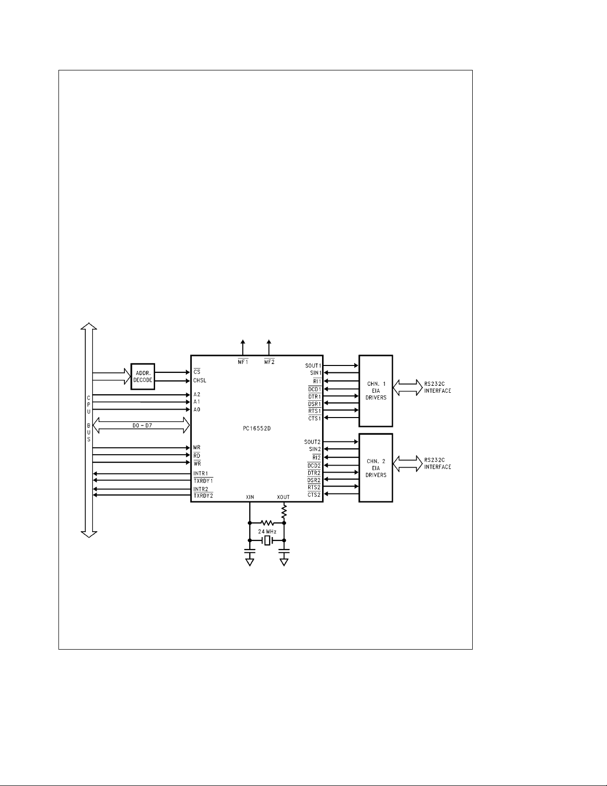
Table of Contents
1.0 ABSOLUTE MAXIMUM RATINGS
2.0 DC ELECTRICAL CHARACTERISTICS
3.0 AC ELECTRICAL CHARACTERISTICS
4.0 TIMING WAVEFORMS
5.0 BLOCK DIAGRAM OF A SINGLE SERIAL CHANNEL
6.0 PIN DESCRIPTIONS
6.1 Input Signals
6.2 Output Signals
6.3 Input/Output Signals
6.4 Clock Signals
6.5 Power
7.0 CONNECTION DIAGRAM
8.0 REGISTERS
8.1 Line Control Register
8.2 Typical Clock Circuits
Basic Configuration
8.0 REGISTERS (Continued)
8.3 Programmable Baud Generator
8.4 Line Status Register
8.5 FIFO Control Register
8.6 Interrupt Identification Register
8.7 Interrupt Enable Register
8.8 Modem Control Register
8.9 Modem Status Register
8.10 Alternate Function Register
8.11 Scratchpad Register
9.0 FIFO Mode Operation
9.1 FIFO Interrupt Operation
9.2 FIFO Polled Operation
10.0 ORDERING INFORMATION
TL/C/9426– 1
2
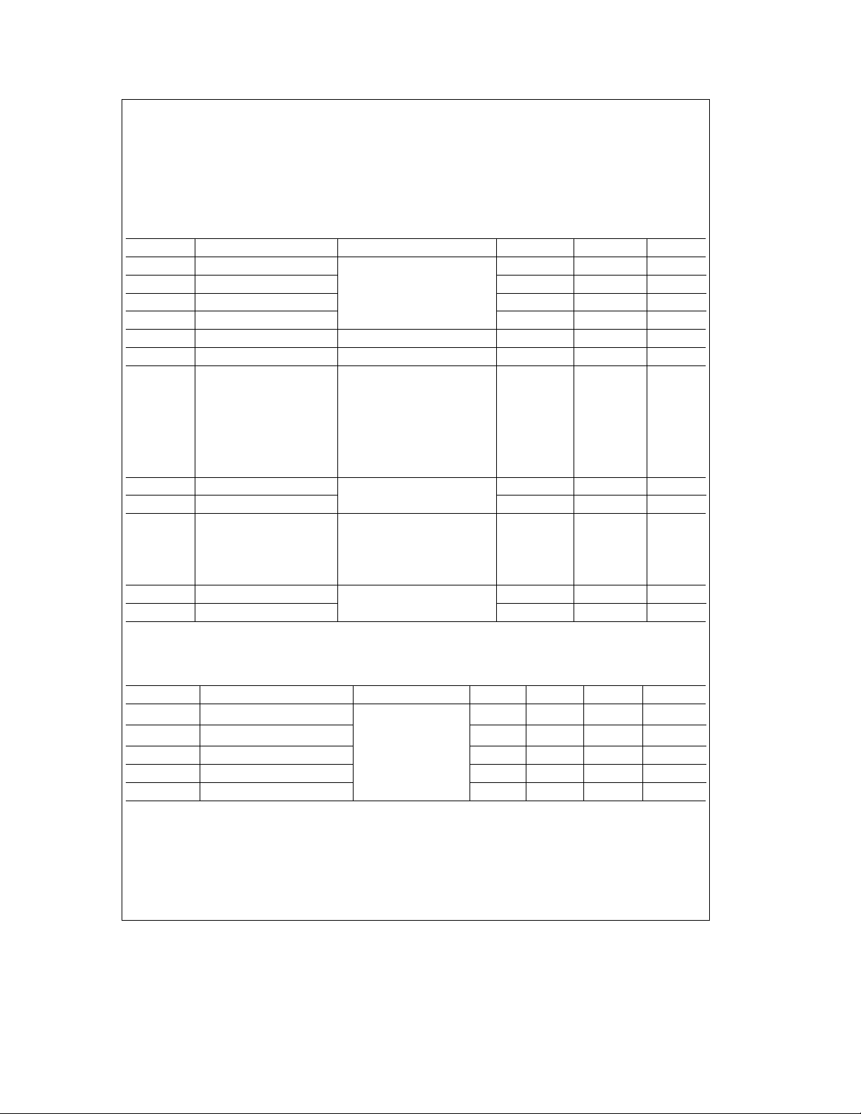
1.0 Absolute Maximum Ratings
Temperature under Bias 0§Ctoa70§C
Storage Temperature
All Input or Output Voltages
with Respect to V
SS
b
65§Ctoa150§C
b
0.5V toa7.0V
Power Dissipation 1W
2.0 DC Electrical Characteristics
e
T
0§Ctoa70§C, V
A
DD
ea
5Vg10%, V
e
0V, unless otherwise specified
SS
Symbol Parameter Conditions Min Max Units
V
ILX
V
IHX
V
IL
V
IH
V
OL
V
OH
ICC(AV) Average Power Supply V
Clock Input Low Voltage
Clock Input High Voltage 2 V
Input Low Voltage
Input High Voltage 2 V
Output Low Voltage I
Output High Voltage I
Current No Loads on Output;
e
1.6 mA on all (Note 1) 0.4 V
OL
eb
1 mA (Note 1) 2.4 V
OH
e
5.5V
DD
CS, RD, WR,
SIN, DSR, DCD,
e
CTS, RI
2V
All Other Inputse0.8V
e
XIN
24 MHz
e
Divisor
I
IL
I
CL
I
OZ
Input Leakage V
Clock Leakage
TRI-STATE Leakage V
V
V
EFFF
e
5.5V, V
DD
e
0V, 5.5V
IN
e
5.5V, V
DD
e
0V, 5.5V
OUT
1) Chip Deselected
2) WRITE Mode,
Chip Selected
V
ILMR
V
IHMR
Note 1: Does not apply to XOUT
Note 2: T
e
A
MR Schmitt V
MR Schmitt V
25§C
IL
IH
Maximum ratings indicate limits beyond which perma-
Note:
nent damage may occur. Continuous operation at these limits is not intended and should be limited to those conditions
specified under DC electrical characteristics.
b
0.5 0.8 V
CC
b
0.5 0.8 V
CC
30 mA
e
0V
SS
e
0V
SS
g
10 mA
g
10 mA
g
20 mA
0.8 V
2V
V
V
Capacitance T
A
e
25§C, V
DD
e
e
V
0V
SS
Symbol Parameter Conditions Min Typ Max Units
C
C
C
C
C
XIN
XOUT
IN
OUT
I/O
Clock Input Capacitance 7 9 pF
e
f
1 MHz
Clock Output Capacitance 7 9 pF
Input Capacitance 5 7 pF
c
Unmeasured Pins
Returned to V
SS
Output Capacitance 6 8 pF
Input/Output Capacitance 10 12 pF
3
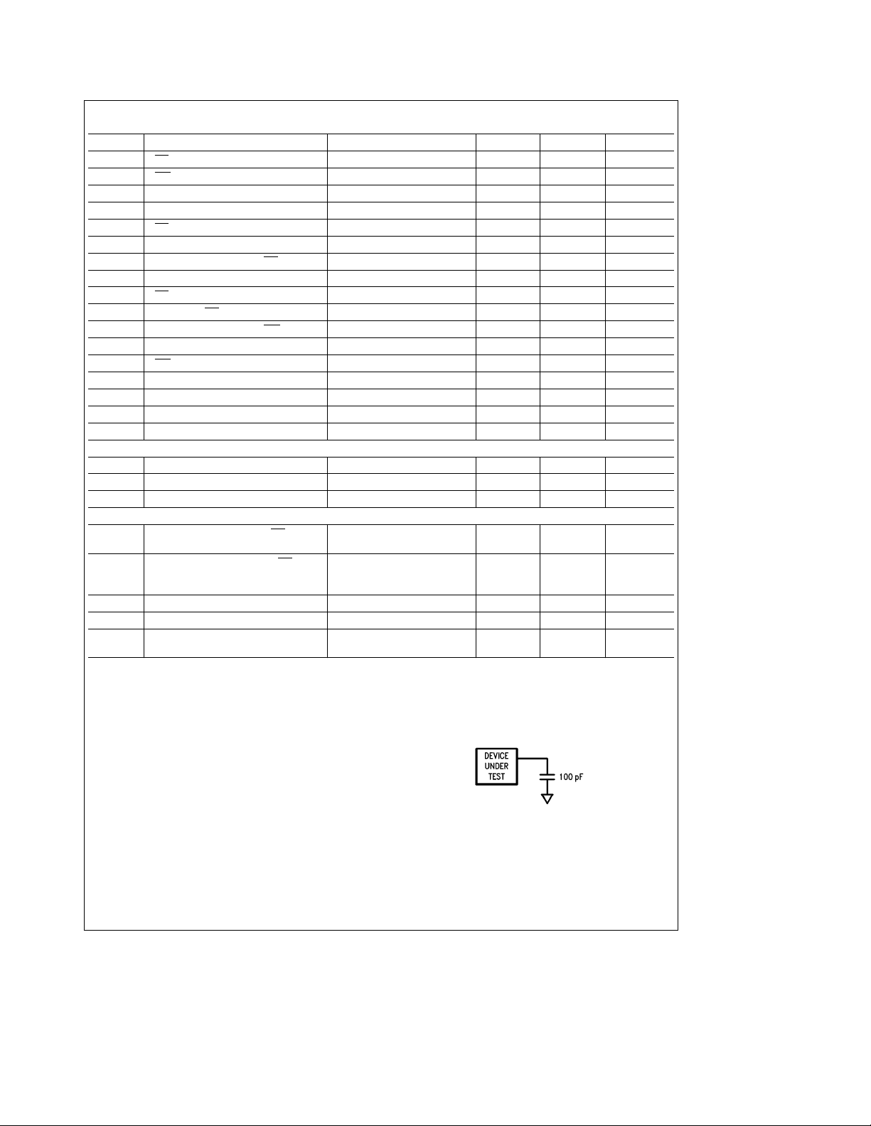
3.0 AC Electrical Characteristics T
e
0§Ctoa70§C, V
A
DD
ea
5Vg10%
Symbol Parameter Conditions Min Max Units
t
AR
t
AW
t
DH
t
DS
t
HZ
t
MR
t
RA
t
RC
t
RD
t
RVD
t
WA
t
WC
t
WR
t
XH
t
XL
RC Read Cycleet
WC Write Cycleet
RD Delay from Address 15 ns
WR Delay from Address 15 ns
Data Hold Time 5 ns
Data Setup Time 15 ns
RD to Floating Data Delay (Note 2) 10 20 ns
Master Reset Pulse Width 500 ns
Address Hold Time from RD 0ns
Read Cycle Update 29 ns
RD Strobe Width 40 ns
Delay from RD to Data 25 ns
Address Hold Time from WR 0ns
Write Cycle Update 29 ns
WR Strobe Width 40 ns
Duration of Clock High Pulse External Clock (24 MHz Max) 17 ns
Duration of Clock Low Pulse External Clock (24 MHz Max) 17 ns
a
a
t
AR
AW
t
RD
a
RC
a
t
t
WR
WC
84 ns
84 ns
BAUD GENERATOR
16
N Baud Divisor 1 2
t
BHD
t
BLD
Baud Output Positive Edge Delay f
Baud Output Negative Edge Delay f
e
24 MHz,d245ns
X
e
24 MHz,d245ns
X
b
1
RECEIVER
t
RAI
t
RINT
Delay from Active Edge of RD to
Reset Interrupt
78 ns
Delay from Inactive Edge of RD
(RD LSR) 40 ns
to Reset Interrupt
t
RXI
t
SCD
t
SINT
Note 1: In the FIFO mode (FCR0e1) the trigger level interrupts, the receiver data available indication, the active RXRDY indication and the overrun error
indication will be delayed 3 RCLKs. Status indicators (PE, FE, BI) will be delayed 3 RCLKs after the first byte has been received. For subsequently received bytes
these indicators will be updated immediately after RDRBR goes inactive. Timeout interrupt is delayed 8 RCLKs.
Note 2: Charge and discharge time is determined by V
Note 3: All AC timings can be met with current loads that don’t exceed 3.2 mA or
Note 4: For capacitive loads that exceed 100 pF the following typical derating factors should be used:
Delay from READ to RXRDY Inactive 55 ns
Delay from RCLK to Sample Time 33 ns
Delay from Stop to Set Interrupt (Note 1)
and the external loading.
OL,VOH
s
100 pF
150 pF
k
C
150 pF te(0.1 ns/pF)(C
L
k
s
C
200 pF te(0.08 ns/pF)(C
L
I
SINK
I
SOURCE
Limits: I
SOURCE
te(0.5 ns/mA)(I
te(0.5 ns/mA)(I
is negative, I
SINK
b
100 pF)
L
b
L
SINK
SOURCE
s
4.8 mA, I
100 pF)
mA)
mA)
SOURCE
s
b
80 mA at 100 pF capacitive loading.
b
120 mA, C
s
250 pF
L
AC Testing Load Circuit
2
BAUDOUT
TL/C/9426– 22
Cycles
4
3.0 AC Electrical Characteristics T
e
0§Ctoa70§C, V
A
ea
5Vg10% (Continued)
DD
Symbol Parameter Conditions Min Max Units
TRANSMITTER
t
HR
t
IR
t
IRS
t
SI
t
STI
t
SXA
t
WXI
Delay from WR (WR THR)
to Reset Interrupt
Delay from RD (RD IIR) to Reset
Interrupt (THRE)
Delay from Initial INTR Reset
to Transmit Start Cycles
Delay from Initial Write to Interrupt (Note 1)
824
16 24
Delay from Start to Interrupt (THRE) (Note 1)
Delay from Start to TXRDY Active
40 ns
40 ns
BAUDOUT
BAUDOUT
Cycles
8
8
BAUDOUT
Cycles
BAUDOUT
Cycles
Delay from Write to TXRDY Inactive 25 ns
MODEM CONTROL
t
MDO
t
RIM
t
SIM
Note 1: This delay will be lengthened by 1 character time, minus the last stop bit time if the transmitter interrupt delay circuit is active. (See FIFO Interrupt Mode
Operation).
Delay from WR (WR MCR)
to Output
Delay to Reset Interrupt from
(RD MSR)
RD
40 ns
78 ns
Delay to Set Interrupt from MODEM Input 40 ns
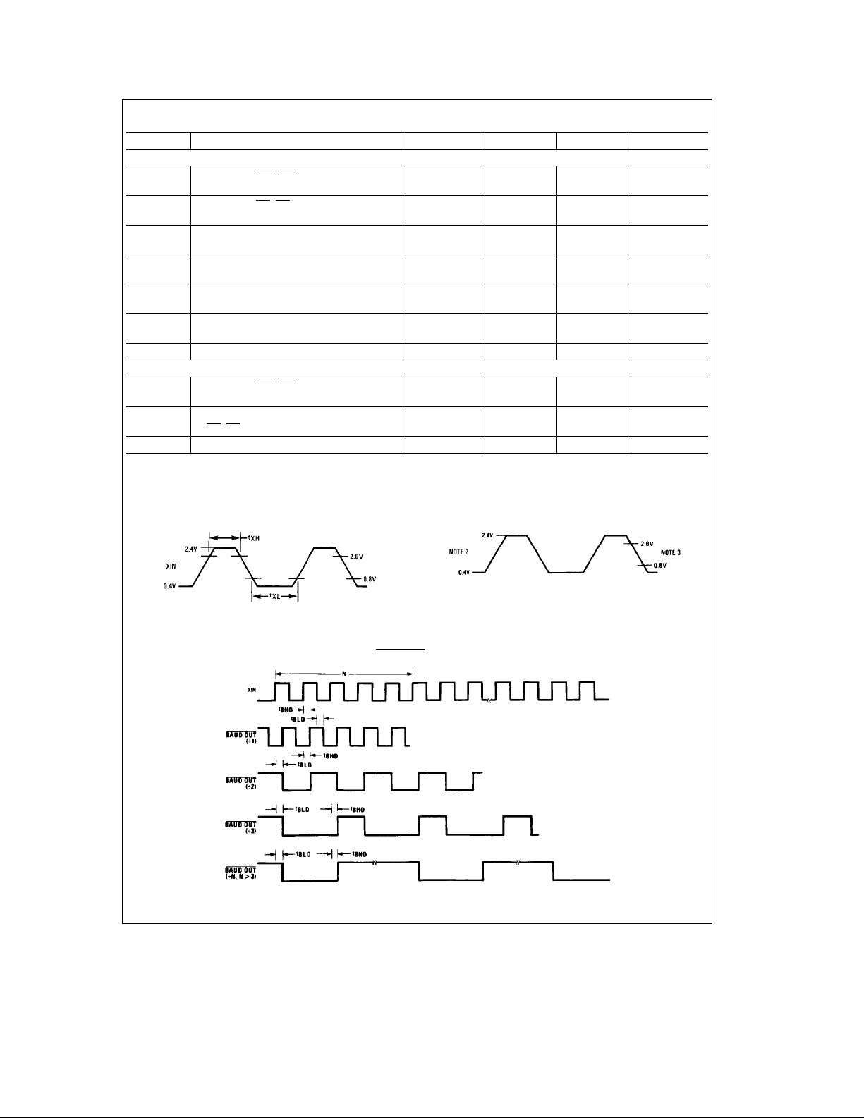
4.0 Timing Waveforms All timings are referenced to valid 0 and valid 1
External Clock Input (24 MHz Max)
AC Test Points
Note 2: The 2.4V and 0.4V levels are the voltages that the inputs are driven to during AC testing.
Note 3: The 2.0V and 0.8V levels are the voltages at which the timing tests are made.
TL/C/9426– 2
BAUDOUT Timing
5
TL/C/9426– 3
TL/C/9426– 4
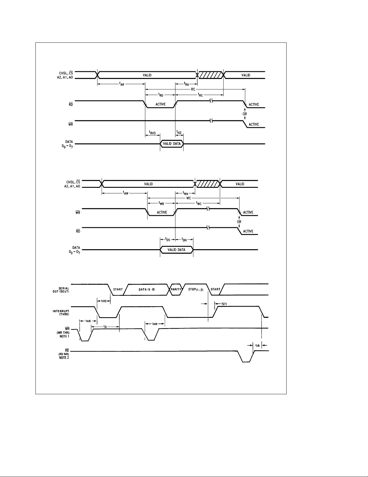
4.0 Timing Waveforms All timings are referenced to valid 0 and valid 1 (Continued)
Read Cycle
Write Cycle
TL/C/9426– 6
Note 1: See Write Cycle Timing.
Note 2: See Read Cycle Timing.
TL/C/9426– 5
Transmitter Timing
TL/C/9426– 8
6
4.0 Timing Waveforms All timings are referenced to valid 0 and valid 1 (Continued)
Receiver Timing
MODEM Control Timing
TL/C/9426– 7
Note 1: See Write Cycle Timing.
Note 2: See Read Cycle Timing.
TL/C/9426– 9
7

4.0 Timing Waveforms All timings are referenced to valid 0 and valid 1 (Continued)
RCVR FIFO First Byte (This Sets RDR)
RCVR FIFO Bytes Other Than the First Byte (RDR Is Already Set)
TL/C/9426– 10
Receiver Ready FCR0e0 or FCR0e1 and FCR3e0 (Mode 0)
Note 1: This is the reading of the last byte in the FIFO.
Note 2: If FCR0
e
1, then t
e
3 RCLKs. For a timeout interrupt, t
SINT
SINT
e
8 RCLKs.
8
TL/C/9426– 11
TL/C/9426– 12

4.0 Timing Waveforms All timings are referenced to valid 0 and valid 1 (Continued)
e
Receiver Ready FCR0
1 and FCR3e1 (Mode 1)
Note 1: This is the reading of the last byte in the FIFO.
Note 2: If FCR0
e
e
1, t
3 RCLKs.
SINT
Transmitter Ready FCR0e0 or FCR0e1 and FCR3e0 (Mode 0)
Transmitter Ready FCR0e1 and FCR3e1 (Mode 1)
TL/C/9426– 13
TL/C/9426– 14
TL/C/9426– 15
9

5.0 Block Diagram of a Single Channel
TL/C/9426– 16
10

6.0 Pin Descriptions
The following describes the function of all DUART pins.
Some of these descriptions reference internal circuits.
In the following descriptions, a low represents a logic 0 (0V
nominal) and a high represents a logic 1 (
Serial channels are designated by a numerical suffix (1 or 2)
after each pin name. If a numerical suffix is not associated
with the pin name, then the information applies to both
channels.
A0, A1, A2 (Register Select), pins 10, 14, 15: Address signals connected to these 3 inputs select a DUART register
for the CPU to read from or write to during data transfer.
Table I shows the registers and their addresses. Note that
the state of the Divisor Latch Access Bit (DLAB), which is
the most significant bit of the Line Control Register, affects
the selection of certain DUART registers. The DLAB must
be set high by the system software to access the Baud
Generator Divisor Latches and the Alternate Function Register.
CHSL (Channel Select), pin 16: This directs the address
and data information to the selected serial channel. When
CHSL is high, channel 1 is selected. When CHSL is low
channel 2 is selected.
CS
(Chip Select), pin 18: When CS is low, the chip is selected. This enables communication between the DUART and
the CPU. Valid chip selects should stabilize according to the
t
parameter.
AW
CTS1, CTS2 (Clear to Send), pins 40, 28: When low, this
indicates that the MODEM or data set is ready to exchange
data. The CTS
signal is a MODEM status input whose condition the CPU can test by reading bit 4 (CTS) of the
MODEM Status Register for the appropriate channel. Bit 4
is the complement of the CTS
signal. Bit 0 (DCTS) of the
MODEM Status Register indicates whether the CTS
has changed state since the previous reading of the
MODEM Status Register. CTS
has no effect on the Trans-
mitter.
Note: Whenever the CTS bit of the MODEM Status Register changes state,
an interrupt is generated if the MODEM Status Interrupt is enabled.
D7–D0(Data Bus), pins 9 –2: This bus comprises eight TRI-
STATE input/output lines. The bus provides bidirectional
communications between the UART and the CPU. Data,
control words, and status information are transferred via the
D
Data Bus.
7–D0
DCD1, DCD2 (Data Carrier Detect), pins 42, 30: When low,
indicates that the data carrier has been detected by the
MODEM or data set. The DCD
signal is a MODEM status
input whose condition the CPU can test by reading bit 7
(DCD) of the MODEM Status Register for the appropriate
channel. Bit 7 is the complement of the DCD
(DDCD) of the MODEM Status Register indicates whether
the DCD
input has changed state since the previous reading
of the MODEM Status Register. DCD
receiver.
Note: Whenever the DCD bit of the MODEM Status Register changes state,
an interrupt is generated if the MODEM Status Interrupt is enabled.
DSR1, DSR2 (Data Set Ready), pins 41, 29: When low, this
indicates that the MODEM or data set is ready to establish
the communications link with the DUART. The DSR
a MODEM status input whose condition the CPU can test by
reading bit 5 (DSR) of the MODEM Status Register for the
a
2.4V nominal).
input
signal. Bit 3
has no effect on the
signal is
appropriate channel. Bit 5 is the complement of the DSR
signal. Bit 1 (DDSR) of the MODEM Status Register indicates whether the DSR
input has changed state since the
previous reading of the MODEM Status Register.
Note: Whenever the DSR bit of the MODEM Status Register changes state,
an interrupt is generated if the MODEM Status Interrupt is enabled.
DTR1, DTR2 (Data Terminal Ready), pins 37, 27: When low,
this informs the MODEM or data set that the DUART is
ready to establish a communications link. The DTR
output
signal can be set to an active low by programming bit 0
(DTR) of the MODEM Control Register to a high level. A
Master Reset operation sets this signal to its inactive (high)
state. Loop mode operation holds this signal in its inactive
state.
INTR1, INTR2 (Interrupt), pins 34, 17: This goes high whenever any one of the following interrupt types has an active
high condition and is enabled via the IER: Receiver Error
Flag; Received Data Available: timeout (FIFO Mode only);
Transmitter Holding Register Empty; and MODEM Status.
The INTR signal is reset low upon the appropriate interrupt
service or a Master Reset operation.
MF1
, MF2 (Multi-Function), pins 35, 19: This can be pro-
grammed for any one of three signal functions OUT 2
BAUDOUT
or RXRDY. Bits 2 and 1 of the Alternate Function Register select which output signal will be present on
this pin. OUT 2
is the default signal and it is selected imme-
diately after master reset or power-up.
The OUT 2
signal can be set active low by programming bit
3 (OUT 2) of the associated channel’s MODEM Control
Register to a 1. A Master Reset operation sets this signal to
its inactive (high) state. Loop Mode holds this signal in its
inactive state.
The BAUDOUT
signal is the 16cclock output that drives
the transmitter and receiver logic of the associated serial
channel. This signal is the result of the XIN clock divided by
the value in the Division Latch Registers. The BAUDOUT
signal for each channel is internally connected to provide
the receiver clock (formerly RCLK on the PC16550D).
The RXRDY
signal can be used to request a DMA transfer
of data from the RCVR FIFO. Details regarding the active
and inactive states of this signal are given in Section 8.5, Bit
3.
MR (Master Reset), pin 21: When this input is high, it clears
all the registers (except the Receiver Buffer, Transmitter
Holding, and Divisor Latches), and the control logic of the
DUART. The states of various output signals (SOUT, INTR,
OUT 2
, RTS, DTR) are affected by an active MR input (Refer to Table III.) This input is buffered with a TTL-compatible
Schmitt Trigger.
RD
(Read), pin 24: When RD is low while the chip is selected, the CPU can read status information or data from the
selected DUART register.
RTS1
, RTS2 (Request to Send), pins 36, 23: When low, this
informs the MODEM or data set that the UART is ready to
exchange data. The RTS
output signal can be set to an
active low by programming bit 1 (RTS) of the MODEM Control Register. A Master Reset operation sets this signal to its
inactive (high) state. Loop mode operation holds this signal
in its inactive state.
,
11

6.0 Pin Descriptions (Continued)
RI1
, RI2 (Ring Indicator), pins 43, 31: When low, this indi-
cates that a telephone ringing signal has been received by
the MODEM or data set. The RI
input whose condition the CPU can test by reading bit 6 (RI)
of the MODEM Status Register for the appropriate channel.
Bit 6 is the complement of the RI
MODEM Status Register indicates whether the RI
nal has changed from a low to a high state since the previous reading of the MODEM Status Register.
Note: Whenever the RI bit of the MODEM Status Register changes from a
high to a low state, an interrupt is generated if the MODEM Status
Interrupt is enabled.
SIN1, SIN2 (Serial Input), pins 39, 25 : Serial data input from
the communications link (peripheral device, MODEM, or
data set).
SOUT1, SOUT2 (Serial Output), pins 38, 26: Composite serial data output to the communications link (peripheral,
MODEM or data set). The SOUT signal is set to the Marking
(logic 1) state upon a Master Reset operation.
TXRDY1
, TXRDY2 (Transmitter Ready), pins 1, 32: Trans-
mitter DMA signalling is available through two pins. When
operating in the FIFO mode, the CPU selects one of
signal is a MODEM status
signal. Bit 2 (TERI) of the
input sig-
7.0 Connection Diagram
Chip Carrier Package
two types of DMA transfer via FCR3. When operating as in
the 16450 Mode, only DMA mode 0 is allowed. Mode 0
supports single transfer DMA where a transfer is made between CPU bus cycles. Mode 1 supports multi-transfer DMA
where multiple transfers are made continuously until the
XMIT FIFO has been filled. Details regarding the active and
inactive states of this signal are given in Section 8.5, Bit 3.
V
(Power), pins 33, 44:a5V Supply
DD
VSS(Ground), pins 12, 22: 0V Reference
WR (Write), pin 20: When WR is low while the chip is select-
ed, the CPU can write control words or data into the selected DUART register.
XIN (External Crystal Input), pin 11: This signal input is used
in conjunction with XOUT to form a feedback circuit for the
baud rate generator’s oscillator. If a clock signal will be generated off-chip, then it should drive the baud rate generator
through this pin.
XOUT (External Crystal Output), pin 13: This signal output is
used in conjunction with XIN to form a feedback circuit for
the baud rate generator’s oscillator. If the clock signal will
be generated off-chip, then this pin is unused.
Top View
Order Number PC16552D
See NS Package Number V44A
12
TL/C/9426– 17

8.0 Registers
TABLE I. Register Addresses
DLAB1 CHSL A2A1A
0 1 0 0 0 Receiver Buffer (Read),
0 1 0 0 1 Interrupt Enable C
0 1 0 1 0 Interrupt Identification (Read) H
0 1 0 1 0 FIFO Control (Write) A
X 1 0 1 1 Line Control N
X 1 1 0 0 MODEM Control N
X 1 1 0 1 Line Status E
X 1 1 1 0 MODEM Status L
X 1 1 1 1 Scratch
1 1 0 0 0 Divisor Latch 1
1 1 0 0 1 Divisor Latch
1 1 0 1 0 Alternate Function
DLAB2 CHSL A2A1A
0 0 0 0 0 Receiver Buffer (Read),
0 0 0 0 1 Interrupt Enable C
0 0 0 1 0 Interrupt Identification (Read) H
0 0 0 1 0 FIFO Control (Write) A
X 0 0 1 1 Line Control N
X 0 1 0 0 MODEM Control N
X 0 1 0 1 Line Status E
X 0 1 1 0 MODEM Status L
X 0 1 1 1 Scratch
1 0 0 0 0 Divisor Latch 2
1 0 0 0 1 Divisor Latch
1 0 0 1 0 Alternate Function
0
Transmitter Holding
Register (Write)
(Least Significant Byte)
(Most Significant Byte)
0
Transmitter Holding
Register (Write)
(Least Significant Byte)
(Most Significant Byte)
Register
Register
13

1
e
1 2 DLAB
e
1 1 DLAB
e
(THRE) (DSR)
Register Ready
Register Address
TABLE II. Register Summary for an Individual Channel
0 2 2 3 4 5 6 7 0 DLAB
e
0 1 DLAB
e
0 0 DLAB
e
Receiver Transmitter Interrupt FIFO
0 DLAB
Only) Only) Only) Only)
(Read (Write Register (Read (Write Register Register Register Register ister (LS) (MS) Register
Bit Buffer Holding Interrupt Ident. Control Line MODEM Line MODEM Scratch Divisor Divisor Alternate
No. Register Register Enable Register Register Control Control Status Status Reg- Latch Latch Function
RBR THR IER IIR FCR LCR MCR LSR MSR SCR DLL DLM AFR
0 Data Bit 0 Data Bit 0 Enable ‘‘0’’ if FIFO Word Data Data Delta Bit 0 Bit 0 Bit 8 Concurrent
Data Pending Select Ready (DR) to Send
(Note 1) Received Interrupt Enable Length Terminal Ready Clear Write
(ERDAI)
Interrupt (WLS0)
Available Bit 0 (DTR) (DCTS)
Holding Bit Reset Select (RTS) (OE) Set
Register Bit 1 Ready
Transmitter ID FIFO Length to Send Error Data Select
1 Data Bit 1 Data Bit 1 Enable Interrupt RCVR Word Request Overrun Delta Bit 1 Bit 1 Bit 9 BAUDOUT
Empty (WLS1) (DDSR)
Interrupt
(ETHREI)
Receiver ID FIFO Stop Bits (Note 3) Error Edge Ring Select
Line Status Bit Reset (STB) (PE) Indicator
2 Data Bit 2 Data Bit 2 Enable Interrupt XMIT Number of Out 1 Parity Trailing Bit 2 Bit 2 Bit 10 RXRDY
14
(ELSI)
Interrupt (TERI)
3 Data Bit 3 Data Bit 3 Enable Interrupt DMA Parity Out 2 Framing Delta Bit 3 Bit 3 Bit 11 0
MODEM ID Mode Enable Error Data
Status Bit Select (PEN) (FE) Carrier
Interrupt (Note 2) Detect
(EMSI) (DDCD)
4 Data Bit 4 Data Bit 4 0 0 Reserved Even Loop Break Clear Bit 4 Bit 4 Bit 12 0
Parity Interrupt to
(EPS) (CTS)
Select (BI) Send
Parity Holding Set
(Note 2) (LSB) (TEMT) (RI)
Enabled Trigger Break Empty Indicator
5 Data Bit 5 Data Bit 5 0 0 Reserved Stick 0 Transmitter Data Bit 5 Bit 5 Bit 13 0
6 Data Bit 6 Data Bit 6 0 FIFOs RCVR Set 0 Transmitter Ring Bit 6 Bit 6 Bit 14 0
7 Data Bit 7 Data Bit 7 0 FIFOs RCVR Divisor 0 Error in Data Bit 7 Bit 7 Bit 15 0
(Note 2) (MSB) Access Bit FIFO Detect
Enabled Trigger Latch RCVR Carrier
(DLAB) (Note 2) (DCD)
Note 1: Bit 0 is the least significant bit. It is the first bit serially transmitted or received.
Note 2: These bits are always 0 in the 16450 Mode.
Note 3: This bit no longer has a pin associated with it.

8.0 Registers (Continued)
Two identical register sets, one for each channel, are in the
DUART. All register descriptions in this section apply to the
register sets in both channels.
8.1 LINE CONTROL REGISTER
The system programmer specifies the format of the asynchronous data communications exchange and sets the Divisor Latch Access bit via the Line Control Register (LCR).
This is a read and write register. Table II shows the contents
of the LCR. Details on each bit follow:
Bits 0 and 1: These two bits specify the number of data bits
in each transmitted or received serial character. The encoding of bits 0 and 1 is as follows:
Bit 1 Bit 0 Data Length
0 0 5 Bits
0 1 6 Bits
1 0 7 Bits
1 1 8 Bits
Bit 2: This bit specifies the number of Stop bits transmitted
with each serial character. If bit 2 is a logic 0, one Stop bit is
generated in the transmitted data. If bit 2 is a logic 1 when a
5-bit data length is selected, one and a half Stop bits are
generated. If bit 2 is a logic 1 when either a 6-, 7-, or 8-bit
word length is selected, two Stop bits are generated. The
receiver checks the first Stop bit only, regardless of the
number of Stop bits selected.
Bit 3: This bit is the Parity Enable bit. When bit 3 is a logic 1,
a Parity bit is generated (transmit data) or checked (receive
data) between the last data bit and Stop bit of the serial
data. (The Parity bit is used to produce an even or odd
number of 1s when the data bits and the Parity bit are
summed.)
Bit 4: This bit is the Even Parity Select bit. When parity is
enabled and bit 4 is a logic 0, an odd number of logic 1s is
transmitted or checked in the data word bits and Parity bit.
When parity is enabled and bit 4 is a logic 1, an even number of logic 1s is transmitted or checked.
Bit 5: This bit is the Stick Parity bit. When parity is enabled it
is used in conjunction with bit 4 to select Mark or Space
Parity. When bits 3, 4 and 5 are logic 1 the Parity bit is
transmitted and checked as a logic 0 (Space Parity). If bits 3
and 5 are 1 and bit 4 is a logic 0 then the Parity bit is
transmitted and checked as a logic 1 (Mark Parity). If bit 5 is
a logic 0 Stick Parity is disabled.
Bit 6: This bit is the Break Control bit. It causes a break
condition to be transmitted to the receiving UART. When it
is set to a logic 1, the serial output (SOUT) is forced to the
Spacing state (logic 0). The break is disabled by setting bit 6
to a logic 0. The Break Control bit acts only on SOUT and
has no effect on the transmitter logic.
Composite Serial Data
Note: This feature enables the CPU to alert a terminal in a computer com-
munications system. If the following sequence is followed, no erroneous or extraneous characters will be transmitted because of the
break.
1. Load an all 0s, pad character, in response to THRE.
2. Set break after the next THRE.
3. Wait for the transmitter to be idle, (TEMT
normal transmission has to be restored.
During the break, the Transmitter can be used as a character timer to accurately establish the break duration.
e
1), and clear break when
Bit 7: This bit is the Divisor Latch Access Bit (DLAB). It must
be set high (logic 1) to access the Divisor Latches of the
Baud Generator or the Alternate Function Register during a
Read or Write operation. It must be set low (logic 0) to access any other register.
8.2 TYPICAL CLOCK CIRCUITS
TL/C/9426– 18
TL/C/9426– 19
Typical Crystal Oscillator Network (Note)
Crystal R
R
P
X2
C
1
C
2
3.1 MHz 1 MX 1.5k 10–30 pF 40 – 60 pF
1.8 MHz 1 MX 1.5k 10–30 pF 40 – 60 pF
Note: These R and C values are approximate and may vary 2 x depending
on the crystal characteristics. All crystal circuits should be designed
specifically for the system.
TL/C/9426– 21
15

8.0 Registers (Continued)
TABLE III. DUART Reset Configuration
Register/Signal Reset Control Reset State
Interrupt Enable Register Master Reset 0000 0000 (Note 1)
Interrupt Identification Register Master Reset 0000 0001
FIFO Control Master Reset 0000 0000
Line Control Register Master Reset 0000 0000
MODEM Control Register Master Reset 0000 0000
Line Status Register Master Reset 0110 0000
MODEM Status Register Master Reset XXXX 0000 (Note 2)
Alternate Function Register Master Reset 0000 0000
SOUT Master Reset High
INTR (RCVR Errs) Read LSR/MR Low
INTR (RCVR Data Ready) Read RBR/MR Low
INTR (THRE) Read IIR/Write THR/MR Low
INTR (Modem Status Changes) Read MSR/MR Low
OUT 2 Master Reset High
RTS Master Reset High
DTR Master Reset High
RCVR FIFO MR/FCR1#FCR0/DFCR0 All Bits Low
XMIT FIFO MR/FCR1#FCR0/DFCR0 All Bits Low
Note 1: Boldface bits are permanently low.
Note 2: Bits 7 –4 are driven by the input signals.
8.3 PROGRAMMABLE BAUD GENERATOR
The DUART contains two independently programmable
Baud Generators. Each is capable of taking a common
clock input from DC to 24.0 MHz and dividing it by any divisor from 1 to 2
recommended with a divisor
frequency of the Baud Generator is 16
[
divisor
16
b
1. The highest input clock frequency
e
1 is 24 MHz. The output
e
Ý
(frequency input)d(baud ratec16)]. The
c
the baud rate,
output of each Baud Generator drives the transmitter and
receiver sections of the associated serial channel. Two 8-bit
latches per channel store the divisor in a 16-bit binary format. These Divisor Latches must be loaded during initialization to ensure proper operation of the Baud Generator.
Upon loading either of the Divisor Latches, a 16-bit Baud
Counter is loaded.
Table IV provides decimal divisors to use with crystal frequencies of 1.8432 MHz, 3.072 MHz and 18.432 MHz. For
baud rates of 38400 and below, the error obtained is minimal. The accuracy of the desired baud rate is dependent on
the crystal frequency chosen. Using a divisor of zero is not
recommended.
8.4 LINE STATUS REGISTER
This register provides status information to the CPU concerning the data transfer. Table II shows the contents of the
Line Status Register. Details on each bit follow:
Bit 0: This bit is the receiver Data Ready (DR) indicator. Bit
0 is set to a logic 1 whenever a complete incoming character has been received and transferred into the Receiver
Buffer Register or the FIFO. Bit 0 is reset to a logic 0 by
reading all of the data in the Receiver Buffer Register or the
FIFO.
Bit 1: This bit is the Overrun Error (OE) indicator. Bit 1 indicates that the next character received was transferred into
the Receiver Buffer Register before the CPU could read the
previously received character. This transfer destroys the
previous character. The OE indicator is set to a logic 1 during the character stop bit time when the overrun condition
exists. It is reset whenever the CPU reads the contents of
the Line Status Register. If the FIFO mode data continues to
fill the FIFO beyond the trigger level, an overrun error will
occur only after the FIFO is full and the next character has
been completely received in the shift register. OE is indicated to the CPU as soon as it happens. The character in the
shift register can be overwritten, but it is not transferred to
the FIFO.
Bit 2: This bit is the Parity Error (PE) indicator. Bit 2 indicates that the received data character does not have the
correct even or odd parity, as selected by the even-parityselect bit. The PE bit is set to a logic 1 during the character
Stop bit time when the character has a parity error. It is
reset to a logic 0 whenever the CPU reads the contents of
the Line Status Register or when the next character is loaded into the Receiver Buffer Register. In the FIFO mode this
error is associated with the particular character in the FIFO
it applies to. This error is revealed to the CPU when its
associated character is at the top of the FIFO.
Bit 3: This bit is the Framing Error (FE) indicator. Bit 3 indicates that the received character did not have a valid Stop
bit. The FE bit is set to a logic 1 when the serial channel
detects a logic 0 during the first Stop bit time. The FE indicator is reset whenever the CPU reads the contents of the
Line Status Register or when the next character is loaded
into the Receiver Buffer Register. In the FIFO Mode this
error is associated with the particular character in the FIFO
it applies to. This error is revealed to the CPU when its
associated character is at the top of the FIFO. The serial
channel will try to resynchronize after a framing error. To do
this it assumes that the framing error was due to the next
start bit, so it samples this ‘‘start’’ bit twice and then takes in
the ‘‘data’’.
16

8.0 Registers (Continued)
Bit 4: This bit is the Break Interrupt (BI) indicator. Bit 4 is set
to a logic 1 whenever the received data input is held in the
Spacing (logic 0) state for longer than a full word transmission time (that is, the total time of Start bit
a
data bits
a
ParityaStop bits). The BI indicator is reset whenever the
CPU reads the contents of the Line Status Register or when
the next valid character is loaded into the Receiver Buffer
Register. In the FIFO Mode this condition is associated with
the particular character in the FIFO it applies to. It is revealed to the CPU when its associated character is at the
top of the FIFO. When break occurs only one zero character
is loaded into the FIFO. The next character transfer is enabled after SIN goes to the marking state and receives the
next valid start bit.
Note: Bits 1 through 4 are the error conditions that produce a Receiver Line
Status interrupt whenever any of the corresponding conditions are
detected and the interrupt is enabled.
Bit 5: This bit is the Transmitter Holding Register Empty
(THRE) indicator. In the 16450 mode bit 5 indicates that the
associated serial channel is ready to accept a new character for transmission. In addition, this bit causes the DUART
to issue an interrupt to the CPU when the Transmit Holding
Register Empty Interrupt enable is set high. The THRE bit is
set to a logic 1 when a character is transferred from the
Transmitter Holding Register into the Transmitter Shift Register. The bit is reset to logic 0 concurrently with the loading
of the Transmitter Holding Register by the CPU. In the FIFO
mode this bit is set when the XMIT FIFO is empty; it is
cleared when at least 1 byte is written to the XMIT FIFO.
Bit 6: This bit is the Transmitter Empty (TEMT) indicator. Bit
6 is set to a logic 1 whenever the Transmitter Holding Register (THR) and the Transmitter Shift Register (TSR) are both
empty. It is reset to a logic 0 whenever either the THR or
TSR contains a data character. In the FIFO mode this bit is
set to one whenever the transmitter FIFO and shift register
are both empty.
TABLE IV. Baud Rates, Divisors and Crystals
1.8432 MHz Crystal 3.072 MHz Crystal 18.432 MHz Crystal
Baud Rate
Decimal Divisor
c
for 16
Clock for 16cClock for 16cClock
Percent Error
Decimal Divisor
50 2304 Ð 3840 Ð 23040 Ð
75 1536 Ð 2560 Ð 15360 Ð
110 1047 0.026 1745 0.026 10473 Ð
134.5 857 0.058 1428 0.034 8565 Ð
150 768 Ð 1280 Ð 7680 Ð
300 384 Ð 640 Ð 3840 Ð
600 192 Ð 320 Ð 1920 Ð
1200 96 Ð 160 Ð 920 Ð
1800 64 Ð 107 0.312 640 Ð
2000 58 0.69 96 Ð 576 Ð
2400 48 Ð 80 Ð 480 Ð
3600 32 Ð 53 0.628 320 Ð
4800 24 Ð 40 Ð 240 Ð
7200 16 Ð 27 1.23 160 Ð
9600 12 Ð 20 Ð 120 Ð
19200 6 Ð 10 Ð 60 Ð
38400 3 Ð 5 Ð 30 Ð
56000 2 2.86 Ð Ð 21 2.04
128000 Ð Ð Ð Ð 9 Ð
Note: For baud rates of 250k, 300k, 375k, 500k, 750k and 1.5M using a 24 MHz crystal causes minimal error.
Bit 7: In the 16450 Mode this is a 0. In the FIFO Mode LSR7
is set when there is at least one parity error, framing error or
break indication in the FIFO. LSR7 is cleared when the CPU
reads the LSR, if there are no subsequent errors in the
FIFO.
Note: The Line Status Register is intended for read operations only. Writing
to this register is not recommended as this operation is only used for
factory testing. In the FIFO mode the user must load a data byte into
the Rx FIFO in order to write to LSR2 –4. LSR0 and LSR7 cannot be
written to in the FIFO mode.
8.5 FIFO CONTROL REGISTER
This is a write only register at the same location as the IIR
(the IIR is a read only register). This register is used to enable the FIFOs, clear the FIFOs, set the RCVR FIFO trigger
level, and select the type of DMA signalling.
Bit 0: Writinga1toFCR0 enables both the XMIT and RCVR
FIFOs. Resetting FCR0 will clear all bytes in both FIFOs.
When changing from FIFO Mode to 16450 Mode and vice
versa, data is automatically cleared from the FIFOs. This bit
must be a 1 when other FCR bits are written to or they will
not be programmed.
Bit 1: Writinga1toFCR1 clears all bytes in the RCVR FIFO
and resets its counter logic to 0. The shift register is not
cleared. The 1 that is written to this bit position is self-clearing.
Bit 2: Writinga1toFCR2 clears all bytes in the XMIT FIFO
and resets its counter logic to 0. The shift register is not
cleared. The 1 that is written to this bit position is self-clearing.
Bit 3: Writinga1toFCR3 causes RXRDY
and TXRDY oper-
ations to change from mode 0 to mode 1 if FCR0
RXRDY Mode 0: When in the 16450 Mode (FCR0e0) or
in the FIFO Mode (FCR0
e
1, FCR3e0) and there is at
least 1 character in the RCVR FIFO or RCVR Buffer Register, the RXRDY
RXRDY
pin will go low active. Once active the
pin will go inactive when there are no more charac-
ters in the FIFO or Buffer Register.
Percent Error
Decimal Divisor
Percent Error
17
e
1.

8.0 Registers (Continued)
e
RXRDY Mode 1: In the FIFO Mode (FCR0
e
FCR3
reached, the RXRDY
vated it will go inactive when there are no more characters
in the FIFO.
TXRDY Mode 0: In the 16450 Mode (FCR0
FIFO Mode (FCR0
characters in the XMIT FIFO or XMIT Holding Register, the
TXRDY
will go inactive after the first character is loaded into the
XMIT FIFO or Holding Register.
TXRDY Mode 1: In the FIFO Mode (FCR0
and when there are no characters in the XMIT FIFO, the
TXRDY
when the XMIT FIFO is completely full.
Bit 4, 5: FCR4 to FCR5 are reserved for future use.
Bit 6, 7: FCR6 and FCR7 are used to designate the interrupt
trigger level. When the number of bytes in the RCVR FIFO
equals the designated interrupt trigger level, a Received
Data Available Interrupt is activated. This interrupt must be
enabled by setting IER0.
FIFO Interrupt
Mode Identification Interrupt Set and Reset Functions
Only Register
Bit 3 Bit 2 Bit 1 Bit 0
0 0 0 1 Ð None None Ð
0 1 1 0 Highest Receiver Line Status Overrun Error or Parity Error or Reading the Line Status
0 1 0 0 Second Received Data Available Receiver Data Available or Trigger Reading the Receiver Buffer
1 1 0 0 Second Character Timeout No Characters Have Been Reading the Receiver
0 0 1 0 Third Transmitter Holding Transmitter Holding Reading the IIR Register (if
0 0 0 0 Fourth MODEM Status Clear to Send or Data Set Ready or Reading the MODEM
1 and the trigger level or the timeout has been
pin will go low active. Once active the TXRDY pin
pin will go low active. This pin will become inactive
FCR Bits RCVR FIFO
7 6 Trigger Level (Bytes)
00 01
01 04
10 08
11 14
pin will go low active. Once it is acti-
e
1, FCR3e0) when there are no
Priority
Level
Indication Buffer Register
Register Empty Register Empty
1) when the
e
0) or in the
e
1, FCR3e1)
TABLE V. Interrupt Control Functions
Interrupt Type Interrupt Source Interrupt Reset Control
8.6 INTERRUPT IDENTIFICATION REGISTER
In order to provide minimum software overhead during data
character transfers, each serial channel of the DUART prioritizes interrupts into four levels and records these in the
Interrupt Identification Register. The four levels of interrupt
conditions in order of priority are Receiver Line Status; Received Data Ready; Transmitter Holding Register Empty;
and MODEM Status.
When the CPU reads the IIR, the associated DUART serial
channel freezes all interrupts and indicates the highest priority pending interrupt to the CPU. While this CPU access is
occurring, the associated DUART serial channel records
new interrupts, but does not change its current indication
until the access is complete. Table II shows the contents of
the IIR. Details on each bit follow:
Bit 0: This bit can be used in a prioritized interrupt environment to indicate whether an interrupt is pending. When bit 0
is a logic 0, an interrupt is pending and the IIR contents may
be used as a pointer to the appropriate interrupt service
routine. When bit 0 is a logic 1, no interrupt is pending.
Bits 1 and 2: These two bits of the IIR identify the highest
priority interrupt pending from those shown in Table V.
Bit 3: In the 16450 Mode this bit is 0. In the FIFO Mode this
bit is set along with bit 2 when a timeout interrupt is pending.
Bits 4 and 5: These two bits of the IIR are always logic 0.
Bits 6 and 7: These two bits are set when FCR0
(FIFO Mode enabled.)
Framing Error or Break Interrupt Register
Level Reached Register or the FIFO Drops
Removed from or Input to the
RCVR FIFO During the Last 4 Char.
Times and There is at Least 1 Char.
in it During This Time
Ring Indicator or Data Carrier
Detect
below the Trigger Level
Source of Interrupt) or Writing
into the Transmitter Holding
Register
Status Register
e
1.
18

8.0 Registers (Continued)
8.7 INTERRUPT ENABLE REGISTER
This register enables five types of interrupts for the associated serial channel. Each interrupt can individually activate
the interrupt (INTR) output signal. It is possible to totally
disable the interrupt system by resetting bits 0 through 3 of
the Interrupt Enable Register (IER). Similarly, setting bits of
the IER register to a logic 1, enables the selected interrupt(s). Disabling an interrupt prevents it from being indicated as active in the IIR and from activating the INTR output
signal. All other system functions operate in their normal
manner, including the setting of the Line Status and
MODEM Status Registers. Table II shows the contents of
the IER. Details on each bit follow:
Bit 0: When set to logic 1 this bit enables the Received Data
Available Interrupt and Timeout Interrupt in the FIFO Mode.
Bit 1: When set to logic 1 this bit enables the Transmitter
Holding Register Empty Interrupt.
Bit 2: When set to logic 1 this bit enables the Receiver Line
Status Interrupt.
Bit 3: When set to logic 1 this bit enables the MODEM
Status Interrupt.
Bits 4 through 7: These four bits are always logic 0.
8.8 MODEM CONTROL REGISTER
This register controls the interface with the MODEM or data
set (or a peripheral device emulating a MODEM). The contents of the MODEM Control Register are indicated in Table
II and are described below:
Bit 0: This bit controls the Data Terminal Ready (DTR
put. When bit 0 is set to a logic 1, the DTR
to a logic 0. When bit 0 is reset to a logic 0, the DTR
is forced to a logic 1.
Bit 1: This bit controls the Request to Send (RTS
Bit 1 affects the RTS
described above for bit 0.
Bit 2: This bit is the OUT 1
pin associated with it. It can be written to and read by the
CPU. In Local Loopback Mode this bit controls bit 2 of the
Modem Status Register.
Bit 3: This bit controls the Output 2 (OUT 2
an auxiliary user-designated output. Bit 3 affects the OUT 2
pin in a manner identical to that described above for bit 0.
The function of this bit is multiplexed on a single output pin
with two other functions: BAUDOUT
OUT 2
function is the default function of the pin after a
master reset. See Section 8.10 for more information about
selecting one of these 3 pin functions.
Bit 4: This bit provides a local loopback feature for diagnostic testing of the associated serial channel. When bit 4 is set
to logic 1, the following occur: the transmitter Serial Output
(SOUT) is set to the Marking (logic 1) state; the receiver
Serial Input (SIN) is disconnected; the output of the Transmitter Shift Register is ‘‘looped back’’ into the Receiver Shift
Register input; the four MODEM Control inputs (DSR
RI
, and DCD) are disconnected; the four MODEM Control
outputs (DTR
nected to the four MODEM Control inputs; and the MODEM
Control output pins are forced to their inactive state (high).
In this diagnostic mode, data that is transmitted is immediately received. This feature allows the processor to verify
transmit and receive data paths of the DUART.
output in a manner identical to that
bit. It does not have an output
, RTS, OUT 1, and OUT 2) are internally con-
output is forced
) signal, which is
and RXRDY. The
) out-
output
) output.
, CTS,
In this diagnostic mode, the receiver and transmitter interrupts are fully operational. Their sources are external to the
part. The MODEM Control Interrupts are also operational,
but the interrupts’ sources are now the lower four bits of the
MODEM Control Register instead of the four MODEM Control inputs. The interrupts are still controlled by the Interrupt
Enable Register.
Bits 5 through 7: These bits are permanently set to logic 0.
8.9 MODEM STATUS REGISTER
This register provides the current state of the control lines
from the MODEM (or peripheral device) to the CPU. In addition to this current-state information, four bits of the
MODEM Status Register provide change information. The
latter bits are set to a logic 1 whenever a control input from
the MODEM changes state. They are reset to logic 0 whenever the CPU reads the MODEM Status Register.
The contents of the MODEM Status Register are indicated
in Table II and described below.
Bit 0: This bit is the Delta Clear to Send (DCTS) indicator.
Bit 0 indicates that the CTS
state since the last time it was read by the CPU.
Bit 1: This bit is the Delta Data Set Ready (DDSR) indicator.
Bit 1 indicates that the DSR
state since the last time it was read by the CPU.
Bit 2: This bit is the Trailing Edge of Ring Indicator (TERI)
detector. Bit 2 indicates that the RI
changed from a low to a high state.
Bit 3: This bit is the Delta Data Carrier Detect (DDCD) indicator. Bit 3 indicates that the DCD
changed state.
Note: Whenever bit 0, 1, 2, or 3 is set to logic 1, a MODEM Status Interrupt
is generated.
Bit 4: This bit is the complement of the Clear to Send (CTS)
input. If bit 4 (loop) of the MCR is set to a 1, this bit is
equivalent to RTS in the MCR.
Bit 5: This bit is the complement of the Data Set Ready
(DSR
) input. If bit 4 of the MCR is set to a 1, this bit is
equivalent to DTR in the MCR.
Bit 6: This bit is the complement of the Ring Indicator (RI
input. If bit 4 of the MCR is set to a 1, this bit is equivalent to
OUT 1 in the MCR.
Bit 7: This bit is the complement of the Data Carrier Detect
(DCD
) input. If bit 4 of the MCR is set to a 1, this bit is
equivalent to OUT 2 in the MCR.
8.10 ALTERNATE FUNCTION REGISTER
This is a read/write register used to select specific modes of
operation. It is located at address 010 when the DLAB bit is
set.
Bit 0: When this bit is set the CPU can write concurrently to
the same register in both register sets. This function is intended to reduce the DUART initialization time. It can be
used by a CPU when both channels are initialized to the
same state. The CPU can set or clear this bit by accessing
either register set. When this bit is set the channel select pin
still selects the channel to be accessed during read operations. Setting or clearing this bit has no effect on read operations.
The user should ensure that the DLAB bit (LCR7) of both
channels are in the same state before executing a concurrent write to register addresses 0, 1 and 2.
input to the chip has changed
input to the chip has changed
input to the chip has
input to the chip has
)
19

8.0 Registers (Continued)
Bits 1 and 2: These select the output signal that will be
present on the multi-function pin, MF
ually programmable for each channel, so that different signals can be selected on each channel. Table VI associates
the signal present at the multi-function pin with the bit code.
TABLE VI
AFR Bit Code
Bit 2 Bit 1
0 0 (Note 1) OUT 2
0 1 BAUDOUT
1 0 RXRDY
1 1 Reserved (Note 2)
Note 1: This is the state after power-up or master reset.
Note 2: Output is forced high.
Bits 3 through 7: These bits are permanently set to a logic
0.
8.11 SCRATCHPAD REGISTER
This 8-bit Read/Write Register does not control the serial
channel in any way. It is intended as a Scratchpad Register
to be used by the programmer to hold data temporarily.
. These bits are individ-
Multi-Function Pin Signal
9.0 FIFO Mode Operation
Each serial channel has two 16-byte FIFOs associated with
it. The operational description that follows is applicable to
the FIFOs of both channels.
9.1 FIFO INTERRUPT OPERATION
When the RCVR FIFO and receiver interrupt are enabled
e
(FCR0
will occur as follows:
A. The Receive Data Available Interrupt will be issued to the
B. The IIR Receive Data Available Indication also occurs
C. The Receiver Line Status Interrupt (IIR
D. The data ready bit (LSR0) is set as soon as a character is
When RCVR FIFO and receiver interrupts are enabled,
RCVR FIFO timeout interrupts will occur as follows:
A. A RCVR FIFO Timeout Interrupt will occur, if the following
1, IER0e1) Receive Data Available Interrupts
CPU when the number of bytes in the RCVR FIFO equals
the programmed trigger level; it will be cleared as soon
as the number of bytes in the RCVR FIFO drops below its
programmed trigger level.
when the FIFO trigger level is reached, and like the interrupt it is cleared when the FIFO drops below the trigger
level.
has higher priority than the Received Data Available
e
(IIR
04) Interrupt.
transferred from the shift register to the RCVR FIFO. It is
reset when the RCVR FIFO is empty.
conditions exist:
Ð at least one character is in the RCVR FIFO
Ð the most recent serial character received was longer
than 4 continuous character times ago (if 2 stop bits
are programmed the second one is included in this
time delay).
Ð the most recent CPU read of the RCVR FIFO was
longer than 4 continuous character times ago.
e
06), as before,
The maximum time between a received character and a
timeout interrupt will be 160 ms at 300 baud with a 12-bit
receive character (i.e. 1 START, 8 DATA, 1 PARITY and
2 STOP BITS).
B. Character times are calculated by using the BAUDOUT
signal as a clock signal (this makes the delay proportional to the baud rate).
C. When a timeout interrupt has occurred it is cleared and
the timer reset when the CPU reads one character from
the RCVR FIFO.
D. When the timeout interrupt indication is inactive the time-
out indication timer is reset after a new character is received or after the CPU reads the RCVR FIFO.
When the XMIT FIFO interrupts are enabled (FCR0
e
IER1
1), XMIT interrupts will occur as follows:
A. The Transmitter Holding Register Empty Interrupt occurs
when the XMIT FIFO is empty. It is cleared as soon as
the Transmitter Holding Register is written to (1 to 16
characters may be written to the XMIT FIFO while servicing this interrupt) or the IIR is read.
B. The transmitter FIFO empty indications will be delayed 1
character time minus the last Stop bit time whenever the
following occurs: THRE
least two bytes at the same time in the transmit FIFO,
since the last THRE
Register Empty Interrupt after changing FCR0 will be immediate, if it is enabled.
This delay prevents the DUART from issuing a second
Transmitter Holding Register Empty Interrupt as soon as it
transfers the first character into the Transmitter Shift Register.
Character timeout and RCVR FIFO trigger level interrupts
have the same priority as the current received data available interrupt; XMIT FIFO Empty has the same priority as
the current Transmitter Holding Register Empty Interrupt.
9.2 FIFO POLLED OPERATION
With FCR0
zero puts the associated serial channel in the FIFO Polled
Mode of operation. Since the receiver and transmitter are
controlled separately either one or both can be in the polled
mode of operation.
In this mode the user’s program will check receiver and
transmitter status via the LSR. As stated in Section 8.4:
There is no trigger level reached or timeout condition indicated in the FIFO Polled Mode, however, the RCVR and
XMIT FIFOs are otherwise functional.
e
1 resetting IER0, IER1, IER2, IER3 or all to
LSR0 will be set as long as there is one byte in the RCVR
FIFO.
LSR1 to LSR4 will specify which error(s) has occurred.
Character error status is handled the same way as in the
interrupt mode.
LSR5 will indicate when the XMIT FIFO is empty.
LSR6 will indicate that both the XMIT FIFO and shift register are empty.
LSR7 will indicate whether there are any errors in the
RCVR FIFO.
e
1 and there have not been at
e
1. The first Transmitter Holding
e
1,
20

21

Physical Dimensions inches (millimeters)
44-Lead Plastic Chip Carrier (V)
Order Number PC16552DV
NS Package Number V44A
LIFE SUPPORT POLICY
NATIONAL’S PRODUCTS ARE NOT AUTHORIZED FOR USE AS CRITICAL COMPONENTS IN LIFE SUPPORT
DEVICES OR SYSTEMS WITHOUT THE EXPRESS WRITTEN APPROVAL OF THE PRESIDENT OF NATIONAL
SEMICONDUCTOR CORPORATION. As used herein:
PC16552D Dual Universal Asynchronous Receiver/Transmitter with FIFOs
1. Life support devices or systems are devices or 2. A critical component is any component of a life
systems which, (a) are intended for surgical implant support device or system whose failure to perform can
into the body, or (b) support or sustain life, and whose be reasonably expected to cause the failure of the life
failure to perform, when properly used in accordance support device or system, or to affect its safety or
with instructions for use provided in the labeling, can effectiveness.
be reasonably expected to result in a significant injury
to the user.
National Semiconductor National Semiconductor National Semiconductor National Semiconductor National Semiconductores National Semiconductor
Corporation GmbH Japan Ltd. Hong Kong Ltd. Do Brazil Ltda. (Australia) Pty, Ltd.
2900 Semiconductor Drive Livry-Gargan-Str. 10 Sumitomo Chemical 13th Floor, Straight Block, Rue Deputado Lacorda Franco Building 16
P.O. Box 58090 D-82256 F4urstenfeldbruck Engineering Center Ocean Centre, 5 Canton Rd. 120-3A Business Park Drive
Santa Clara, CA 95052-8090 Germany Bldg. 7F Tsimshatsui, Kowloon Sao Paulo-SP Monash Business Park
Tel: 1(800) 272-9959 Tel: (81-41) 35-0 1-7-1, Nakase, Mihama-Ku Hong Kong Brazil 05418-000 Nottinghill, Melbourne
TWX: (910) 339-9240 Telex: 527649 Chiba-City, Tel: (852) 2737-1600 Tel: (55-11) 212-5066 Victoria 3168 Australia
National does not assume any responsibility for use of any circuitry described, no circuit patent licenses are implied and National reserves the right at any time without notice to change said circuitry and specifications.
Fax: (81-41) 35-1 Ciba Prefecture 261 Fax: (852) 2736-9960 Telex: 391-1131931 NSBR BR Tel: (3) 558-9999
Tel: (043) 299-2300 Fax: (55-11) 212-1181 Fax: (3) 558-9998
Fax: (043) 299-2500
 Loading...