

Page 1

PC16552C Dual UART/DMA
Micro Channel Adapter
Table Of Contents
INTRODUCTION AND FEATURES
PC16552C ADAPTER BLOCK DIAGRAM
PC16552C ADAPTER USER’S GUIDE
POSÐPROGRAMMABLE OPTION SELECT
An overview of the Micro Channel Programmable Option
Select (POS), a unique feature which replaces all adapter
jumpers and switches with programmable configuration registers.
A. POS Mechanism
B. Adapter Description File (ADF)
C. Configuration Utilities
D. POS Registers
E. PC16552C Adapter POS Register Design
MICRO CHANNEL BUS INTERFACE
General information on the adapter interface to the Micro
Channel, applicable to any adapter design, and specific information on the design of the PC16552C Adapter.
A. Micro Channel Control Signals
B. Data Bus
C. Address Decode
D. UART Interface
E. Interrupts
MICRO CHANNEL BUS ARBITRATION
An overview of the bus arbitration system implemented on
all Micro Channel machines.
A. Central Arbiter
B. Local Arbiter
PC16552C ADAPTER DMA INTERFACE DESIGN
The design of the PC16552C Adapter’s Local Arbiter and
interface to the UART DMA request signals is described in
detail.
A. Design Considerations
B. DMA Request Enable
C. DMA Request Prioritization
D. Arbitration Vector Selection
E. Local Arbiter
F. Fairness
G. Terminal Count Interrupt
SOFTWARE
A. Programming the Micro Channel DMA Controller
B. Driver Programs
EISA BUS DESIGN COMPARISON
Brief description of a possible EISA bus serial port/DMA
design.
APPENDICES
A. ADF Listing (
B. PAL
Equations
É
@
6e6D.adf)
National Semiconductor
Application Note 770
Greg DeJager
July 1991
APPENDICES (Continued)
C. Schematics
D. Layout Drawing
E. Bill of Materials
INTRODUCTION
The PC16552C integrates two NS16550AF UARTs into a
single package. The product provides control for two independent PC-AT
dition, the on-board FIFOs and DMA request strobes of the
PC16552C create the basis for a high-performance serial
port design.
Advancing modem technology is causing a substantial increase in serial transfer baud rates, putting a severe strain
on existing serial port designs. Personal computer systems
are unable to keep up with transfer rates that are now
reaching 115k baud. The PC16552C allows the serial port
designer to design ports that can handle these faster data
rates. Transmitter and Receiver FIFOs buffer up to 16 bytes
of data each, and request strobes signal the system DMA
controller to transfer data
from
full receiver FIFOs. DMA burst transfers can move
data from the serial I/O ports to system RAM very quickly
with no latency time and no attention from the system CPU.
This document contains a user’s guide for the adapter and
discusses the considerations involved in designing any Micro Channel Adapter equipped with a DMA slave. It gives an
overview of the Micro Channel POS mechanism, adapter
interface and bus arbitration system. The design of the
PC16552C Serial/DMA Adapter, intended as an example of
a DMA slave serial adapter, is described in detail. A descripton of the software necessary to facilitate four simultaneous
file transfers serviced by the Micro Channel DMA controller
is also included.
PC16552C ADAPTER FEATURES
Two independent PC-AT and PS/2 compatible serial
#
ports with FIFOs capable of running all existing NS16450
and NS16550AF software.
All configuration done through POS mechanism. No
#
hardware jumpers or switches.
Serial ports relocatable to all eight standard I/O address-
#
es.
Serial interrupts available on IRQ3 and IRQ4.
#
Hardware interface between UART FIFO DMA requests
#
and the Micro Channel bus arbitration and DMA system.
POS configurable priority levels for UART DMA requests.
#
Support for software enable/disable of UART DMA re-
#
quests.
POS configurable Fairness feature for UART DMA re-
#
quests.
Automatic interrupt generation and DMA request disable
#
upon receipt of DMA Terminal Count.
Two DB-9 connectors for the two RS-232 compatible se-
#
rial ports.
and PS/2Écompatible serial ports. In ad-
É
to
empty transmitter FIFOs and
PC16552C Dual UART/DMA Micro Channel Adapter AN-770
C
1995 National Semiconductor Corporation RRD-B30M75/Printed in U. S. A.
TL/F/11195
Page 2
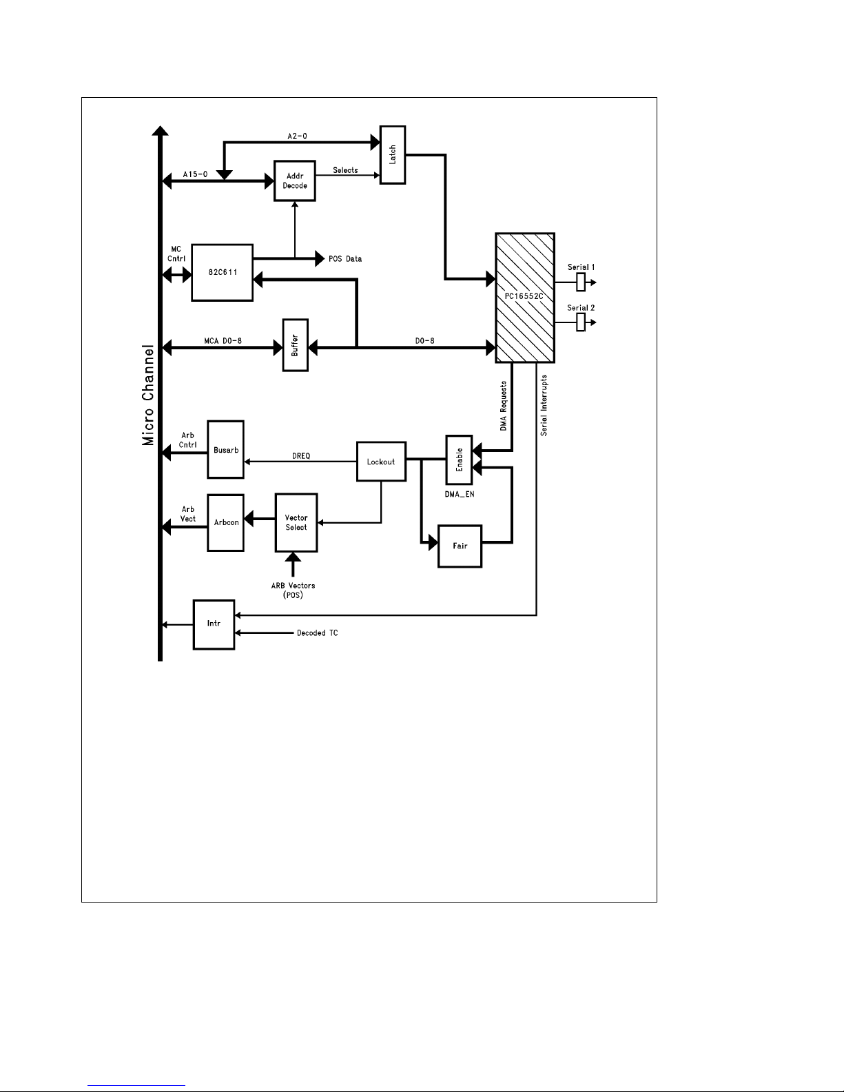
PC16552C Adapter Block Diagram
TL/F/11195– 1
2
Page 3

PC16552C ADAPTER USER’S GUIDE
The PC16552C Adapter comes with a 3(/2
contains the ADF file for the adapter. The file is called
@
6e6d.adf and must be used to configure the adapter. Copy
diskette which
×
the file onto the Reference Diskette (actually the user’s
copy of the Diskette) for the machine to be used. To configure the adapter, plug it into an expansion slot and power up
the machine with the user’s reference diskette inserted in
the A drive. The configuration utility is menu driven and is
simple to follow. Use the manual configuration to see all the
different options available.
The DMA demo programs included on the Adapter’s diskette require that it be configured with Channel 1 on COM2
and Channel 2 on COM3. The priority of the DMA requests
must be configured with Channel 1 Receiver at level 0 (highest priority), Channel 2 Receiver at level 1 and Channel 1
Transmitter at level 6. The Transmitter for Channel 2 defaults to level 7. The Fairness feature should be enabled at
all times except for evaluation purposes.
When the card has been configured and the configuration
has been saved to the system’s CMOS RAM, remove the
Reference Diskette and reboot. The two serial ports may
then be evaluated and tested as any other 16550AF port
would be tested. To demonstrate the DMA transfers, run the
included sample demo programs.
POSÐPROGRAMMABLE OPTION SELECT
A unique feature of Micro Channel machines is their Programmable Option Select, known as POS. POS eliminates
switches and jumpers from adapter cards by replacing their
function with programmable registers. The POS registers allow the system microprocessor to poll each adapter card to
determine its characteristics as well as write configuration
data to it. All resources required by an adapter (memory and
I/O addresses, interrupts used, DMA arbitration vectors,
etc.) can be relocatable and reconfigurable by the POS system. Additionally, each card stores in POS registers a
unique ID number that the POS system uses to identify the
cards present in the system. A full understanding of the
POS mechanism is necessary before an adapter design is
undertaken. The IBM Technical Reference Manuals provide
details about POS that this document may not provide.
POS Mechanism
Each connector slot in the Micro Channel has a unique signal called CDSETUP
that when asserted, puts the card resident in that slot in setup mode. The setup mode allows
access to a block of 8 POS registers located at I/O addresses 100h –107h. All cards in the system locate their
POS registers in this space but since only one card can be
placed in setup at a time, no conflicts can occur.
Micro Channel machines store in battery-backed CMOS
RAM the ID numbers of all resident adapters, the slot numbers they’re plugged into and the configuration data to be
written to their respective POS registers. During Power On
Self Test (POST), the system microprocessor puts each slot
in turn into setup mode and reads its ID. If it finds a valid ID
it sends the card its configuration data. If there is no card in
a slot, the microprocessor will read an ffH which it recognizes as an empty slot.
Since the system remembers which adapter and ID resides
in each slot, removing a card, inserting a new card, or even
moving an existing card to a different slot will cause a POST
failure. IBM’s System Configuration utilities must then be run
to reconfigure the system by modifying the configuration
data stored in CMOS RAM.
ADFsÐAdapter Description Files
System board and adapter POS data is also stored on the
Reference diskette in the form of Adapter Description Files.
ADFs are given names corresponding to the ID of the card it
is to configure. The PC16552C Adapter has an ID number of
6E6Dh, giving it an ADF name of
@
6E6D.adf is included with this documentation.
@
6E6D.adf. A listing of
The ADF is divided into sections which each list one or
more choices of resources to be allocated to the adapter
card. A given choice specifies the data to be loaded into a
particular POS register and also lists the resources allocated. For example, in
@
6E6D.adf, choosing ‘‘Serial 2’’
(COM2) for connector 1 will reserve the I/O address space
2f8–2ffh and will notify the system that IRQ3 is used. It also
specifies the data to be written to some of the bits in POS
registers 102 and 103. Note that pos[0]denotes POS102
and pos[1]denotes POS103 because registers POS100
and 101 contain the read-only card ID bytes which are not
referred to in ADFs. See PC16552C Adapter POS Register
Description for a description of the contents of the registers
used in this adapter.
The syntax for the ADF is straight forward and described in
detail in IBM’s Technical Reference manual. However, the
Configuration utilities are unforgiving of errors. Any errors in
a designer’s ADF will prevent any POS data for that card
from being loaded and the card from being enabled for operation. In addition, the system will not boot to the operating
system while the new card is inserted until the ADF is correct and the system has been reconfigured with the new
data. One undocumented idiosyncrasy involves the 4-bit
fields for arbitration vectors. Since the system DMA controller only recognizes vectors 0–7, only 3 bits are needed to
specify the vectors to be used on the card. However, the
Configuration utilities required that all four bits be specified,
including the most significant bit which is always 0.
Configuration Utilities
There are two different utilities on the Reference diskette
provided with the system which actually convert the ADFs to
configuration data in CMOS RAM. One of these utilities
must be run whenever a new card is installed. The first is
the Automatic Configuration program. It takes the first
choice in each resource list that will not cause a conflict with
other adapters in the system and automatically stores the
corresponding POS register data in CMOS RAM.
The second program is Set Configuration which allows the
user to manually select the resources desired. It first reads
the configuration data already in CMOS RAM and displays
the resources allocated to each installed card. It then allows
the user to change these choices of resources by displaying
one-by-one all of the options for that adapter listed in the
ADFs. After all new choices have been made, exiting the
program causes the new POS data to be loaded into CMOS
RAM and the system is reconfigured and re-booted.
3
Page 4

POS Registers
Address (hex) Function
0100 (POS Register 100) Adapter Identification Byte (LSB)
0101 (POS Register 101) Adapter Identification Byte (MSB)
0102 (POS Register 102) General Option Select Data
0103 (POS Register 103) General Option Select Data
0104 (POS Register 104) General Option Select Data
0105 (POS Register 105) General Option Select Data
0106 (POS Register 106) Sub Address Extension (LSB)
0107 (POS Register 107) Sub Address Extension (MSB)
Registers 100 and 101 are read-only and registers 102 –107
are read and write. The ID registers are required on all
adapters, but all bits in registers 102– 105 are optional and
user-defined except for the following:
102 Bit 0: Card Enable (CDEN): This bit must be imple-
#
mented and is used to enable the entire adapter card. It
is set last during POS initialization and only if the card will
not produce any resource conflicts. The CDEN signal
gates the decode of all addresses used on the adapter
as well as any interrupt requests.
105 Bit 7: Channel Check Active Indicator. This bit is
#
required only by adapters which generate CHCK
(see Micro Channel Interface Control Signals). Error handlers need this bit to identify the source of the error signal.
105 Bit 6: Channel Check Status Indicator (STAT). This
#
bit is also required only by adapters supporting CHCK
is used to indicate that channel check status information
is available in POS106 and 107.
PC16552C Serial/DMA Adapter
POS Register Description
The Chips and Technologies 82C611 Micro Channel Interface IC, used to simplify the interface between the
PC16552C Adapter and the Micro Channel, provides good
POS register support. For all 8 POS registers, the 82C611
can be configured to generate read and write strobes for
externally implemented registers or can implement registers
internally. The 82C611 defines how several of the POS bits
used in this adapter were assigned. As can be seen in the
following register descriptions, some bits are available on
external pins while others are used for internal address decoding or to define the operating modes of the 82C611.
POS100 and POS101ÐAdapter ID Bytes
All adapters must store a two-byte ID number in POS registers 100 and 101. IBM specifies that all direct program control adapters (including memory-mapped I/O) have an ID
byte between 6000 and 6FFFh. As previously mentioned,
the ID byte for this adapter is 6E6DH. When POS100 and
101 are read during setup, the 82C611 produces two sepa-
errors
.It
rate read strobesÐ100RD
well as their logical AND, are used by the INTR PAL to pull
down the data bus bits necessary for the CPU to read back
6D from POS100 and 6E from POS101 (see INTR.ABL for
equations). The data bus is pulled up to insure legal high
levels on bits not driven low.
6E6D has been registered at IBM and is guaranteed not to
conflict with any other legitimate adapters. The number to
call to register an ID is 800-426-7763. It is a good idea to
find out what numbers are available before implementing it
in a design as many numbers are already reserved. Numbers that minimize the logic necessary to implement them
have as few logic 0 bits as possible and also have low and
high order bytes that have 0 bits in the same position.
POS102
This register is internal to the 82C611 and has all 8 bits
brought out to pins POS102B1 –7 and CDEN. It is programmed as follows:
102B7: Fairness: (Used to enable IBM’s
Fairness algorithm. See DMA INTERFACE.)
102B6: A7*A6*A4
102B5: A8
102B4: A3
(Address bits providing decode information
for UART channel 1.)
102B3: A7*A6*A4
102B2: A8
102B1: A3
(Address bits providing decode information
for UART Channel 1.)
102B0: CDEN: (See POS Registers.)
POS103
This register is internal to the 82C611. The bits are not available on external pins but instead are compared to 3 input
pins which are connected to address bus bits 14, 13 and 12.
A match produces an output used for the decode of the
UART channels.
102B7: unused
102B6: unused
102B5: A14
102B4: A13
102B3: A12
(Address bits providing decode information
for UART channel 1.)
102B2: A14
102B1: A13
102B0: A12
(Address bits providing decode information
for UART channel 2.)
and 101RD. These signals, as
4
Page 5

POS104
This register stores the bus arbitration vectors for the UART
receiver DMA requests RXRDY1
mented externally using a 74LS374 latch and 74LS245 buffer. The 82C611 decodes reads and writes to the register
during setup and provides the correct strobes. This information is also needed as external signals so they were implemented in a register with corresponding output pins.
102B7: RX2 ARB3
102B6: RX2 ARB2
102B5: RX2 ARB1
102B4: RX2 ARB0
102B3: RX1 ARB3
102B2: RX1 ARB2
102B1: RX1 ARB1
102B0: RX1 ARB0
POS105
This register is implemented internal to the 82C611. The
lower four bits contain the arbitration vector for UART channel 1 transmitter. They were selected for the vector because
output pins were needed. The upper four bits contain control bits for the Micro Channel interface.
105B7: Channel Check Active Indicator. See
POS registers. It is not used in this
adapter.
105B6: Channel Check Status Indicator
(STAT). See POS Registers. It is not used in
this adapter.
105B5: Synchronous Extended Mode: The 82C611
specifies the definition of this bit. It
generates synchronous extended cycles if set
and asynchronous extended cycles if cleared
(see CHRDY
Signals).
105B4: unused
105B3: TX1 ARB3
105B2: TX1 ARB2
105B1: TX1 ARB1
105B0: TX1 ARB0
POS106 and POS107 are not used in this adapter. The subaddressing bits are used to specify the location of a block of
initial program load (IPL) or additional setup information.
MICRO CHANNEL BUS INTERFACE
Micro Channel Control Signals
All of the Micro Channel signals needed to control an 8- or
16-bit adapter are described below. They are all connected
directly to the 82C611 which meets all IBM timing and drive
specifications for those signals.
CD SFDBK
driven low by an adapter to acknowledge to the system
when it decodes a specified address. The 82C611 drives
this signal low when the adapter logic asserts the part’s
CDSEL input. The CDSEL signal is generated by a logical
OR of the unlatched address decodes of both UART channels and the two registers decoded on the adapter for DMA
control and status (see DMA Interface Design).
in Micro Channel Control
: Card Selected Feedback: This signal must be
and RXRDY2. It is imple-
CD DS16
when an adapter requires a 16-bit data transfer. The
82C611 drives this signal as a function of its DS16 input
which is tied high in this design.
CD CHRDY: Card Channel Ready: An adapter which
needs more time to transfer data on the Micro Channel pulls
this signal low (not ready) to extend the current bus cycle.
There are two types of extended cycles: Asynchronous Extended and Synchronous Extended. The difference between them is when the CD CHRDY signal driven back high
(ready). In the synchronous case, CD CHRDY is removed
within 30 ns of the falling edge of CMD
system to extend the cycle 100 ns or 1 wait state. In the
asynchronous case, CD CHRDY is removed at any time by
the adapter providing as many wait states as necessary (the
limit for holding CD CHRDY low is 3 m s). POS105 bit 5 defines which type the 82C611 supports. A single wait state is
needed to support DMA transfers from the PC16552C so
the bit is programmed for synchronous mode. The 82C611
causes an extended cycle when its ADPRDY
serted by the adapter. In this design, the ADPRDY
the same as the CDSEL signal thus causing an extended
cycle to be generated on every access to the Adapter.
CHRESET: Channel Reset: This active high strobe from
the Micro Channel resets devices on adapter cards. It is
connected to the 82C611, PC16552C, and the Busarb,
Lockout and Fair state machines.
CD SETUP
nal low during POS setup. Upon receiving this signal, the
82C611 places the PC16552C Adapter into setup mode by
allowing access to the POS registers.
REFRESH
refresh cycle is occuring on the bus. The refresh cycle looks
like a normal memory read, which the 82C611 will ignore
upon receiving an active REFRESH
CHCK: Channel Check: Adapters assert this signal to indicate a serious error (such as parity) which threatens system
operation. The signal is common to all adapter slots so it
must be driven with an open-collector driver. The 82C611
drives this signal as a function of the ERROR
tied high (inactive) in this design.
S0
into separate I/O read (IOR) and I/O write (IOW) strobes.
Data Bus
A 74LS245 buffer isolates the Adapter’s data bus from the
Micro Channel data bus to prevent excessive loading of Micro Channel bus. Direction and gating during read and write
cycles is controlled by the 82C611’s BUFDIR and BUFENL
signals. The internal bus connects to the PC16552C,
POS104, DMAÐEN and ISR registers (see DMA Interface)
and the INTR PAL (POS ID generator).
: Card Data Size 16: This signal is driven low
. This causes the
signal is as-
signal is
: Card Setup: The Micro Channel drives this sig-
: This system indicates through this signal that a
signal.
input which is
,S1,M/IO and CMD: The 82C611 decodes these signals
5
Page 6
Address Decode
Micro Channel adapters should have their resources relocatable and selectable through the POS mechanism. This
design allows for the two serial channels on board the
PC16552C to be located at any two of the 8 ‘‘standard’’ IBM
serial port addresses. The following table shows those addresses:
COM Port Hex Address Binary Address (A15 –0)
1 03F8 0000 0011 1111 1000
2 02F8 0000 0010 1111 1000
3 3220 0011 0010 0010 0000
4 3228 0011 0010 0010 1000
5 4220 0100 0010 0010 0000
6 4228 0100 0010 0010 1000
7 5220 0101 0010 0010 0000
8 5228 0101 0010 0010 1000
The upper 13 bits of the address must be decoded while the
lower 3 bits, A2– A0, connect directly to the PC16552C to
select one of 8 internal registers of the selected channel. As
can be seen from the binary addresses above, 5 bits stay
the same for the 8 COM ports (A15, A11, A10, A9, A5) and
8 bits must be programmed for the port selected for decode.
Adapter card logic gates ‘‘compress’’ bit fields that are always at the same logic level so that all 13 bits will not need
to be decoded separately. The 82C611 has inadequate address decoding resources so two 74LS521 Comparators,
one for each UART channel, are implemented to compare
compressed bits and some of the address bus bits with POS
programmed bits and hard-wired bits. POS registers 102
and 103 are programmed with the data necessary to decode the two ports selected for use on the adapter (see
POS Register Description). The entire decode works as follows:
Address bits A15, A11 and A10 are always 0. They are compressed to one bit with a NOR gate and compared to a
hard-wired 1 on both comparators.
A9 and A5 are always 1. They are compressed by a NAND
gate to a bit which is compared to a hard-wired 0 by both
comparators.
A7, A6 and A4 are all 0 if the port address is for COM3 –8. A
NAND gate compresses the bits to a signal which is compared to POS102 bit 6 by the channel 1 comparator and to
POS102 bit 3 by the channel 2 comparator. Thus POS102
bit 6 must be programmed toa0ifchannel 1 is to be COM1
or COM2 and toa1ifit’s to be COM3–8. POS102 bit 3 is
programmed similarly for channel 2.
A8isa1intheCOM1 address and 0 in all others. It is
connected directly to both comparators and compared to
POS102 bit 5 and POS102 bit 2 which are programmed for
channel 1 and channel 2 respectively.
A3 equals 1 in COM1, 2, 4, 6 and 8 and equals 0 in COM3, 5
and 7. It is also connected directly to each comparator and
compared to POS102 bit 4 and bit 1 which are programmed
for channel 1 and channel 2 respectively.
A14, A13 and A12 are connected to 82C611 multi-function
pins MFP6, 5 and 4 respectively. They are constantly compared to two bit fields in POS103ÐB5–3 and B2 –0. Bits 5 –
3 are programmed with the A14, A13 and A12 bits expected
for channel 1 and bits 2 –0 with the bits expected for channel 2. The 82C611 will assert MFP3
for channel 1 and will assert MFP2
for channel 2. MFP3
ator and MFP2
Both are compared to a hard-wired 0.
As stated in the POS Register Description, POS102 bit 0 is
the card enable signal CDEN. The signal enables UART
address decode by being compared to a hard-wired 1 on
both comparators (CDEN is 0 until POS102 bit 0 is set).
Finally, the M/IO signal from the Micro Channel is used to
gate both LS521 comparators so that only I/O addresses
are decoded. The two comparators produce active low outputs when an address match is found. These signals are
CS1
and CS2, the selects for the PC16552’s two channels.
The adapter decodes one additional I/O address, 2F7h,
which is the location of the write-only DMAÐEN register
and read-only ISR register (see DMA Interface for register
description). These registers are not relocatable. However,
the I/O resource is ‘‘claimed’’ in the adapter’s ADF so any
conflict with other cards will be caught by POST which will
not enable the card, preventing system damage.
UART Interface
The PC16552C register address bits (A2, A1, A0) and the
CS
outputs of the LS521 comparators are latched into a
74LS373 by the CMD
bus cycle. The latched CS1
produce the PC16552’s CS
the UART is selected by connecting the CS2
UART’s CHSL input which produces the following channel
decode:
CS1 CS2 (CHSL) Channel Selected
01 1
10 2
11 X
The adapter’s address decode logic and the PC16552C cycle time is fast enough to operate with the Micro Channel’s
default bus cycle length. No wait states are needed for access to the UART.
Interrupts
The Micro Channel’s IRQ interrupts are designed as activelow, level-sensitive signals. This simplifies adapter interrupt
sharing logic and reduces transient sensitivity on the interrupt controller while retaining compatibility with existing software. Because IRQ lines are shared, open-collector drivers
or active-low TRI-STATE
to drive the lines.
is connected to the channel 1 compar-
is connected to the channel 2 comparator.
signal and held for the duration of a
drivers must be used by adapters
É
when a match is made
when a match is made
and CS2 signals are ANDed to
signal. The correct channel on
signal to the
6
Page 7

The INTR GALÉon the PC16552C Adapter drives the IRQ3
and IRQ4 signals. INTR inputs the interrupt signals from the
PC16552C (INTR1 and INTR2) and the TC interrupt (see
DMA Interface). INTR will assert IRQ3 if a TC interrupt is
generated or if a UART channel configured as COM2 –8
generates a serial interrupt. It will assert IRQ4 if it receives a
serial interrupt from a channel configured as COM1. INTR
decodes the serial interrupts by using POS102 bits 5 and 2
which store address bit A8 for channels 1 and 2 respectively. A8 is used because it isa1ifCOM1 is being used and a
0 if any other COM port is used. See the included INTR.ABL
listing for the GAL equations.
MICRO CHANNEL BUS ARBITRATION
The PC16552C Dual Serial/DMA Adapter implements the
logic necessary to interface a DMA slave device to the Micro Channel’s bus arbitration system and DMA controller. A
DMA slave adapter must contain a Local Arbiter, as defined
by IBM, in order to compete for the bus and communicate
with the system’s Central Arbiter. The adapter must also
contain any logic necessary to directly support the device
requesting DMA service.
The following material on the DMA Interface discusses the
function of the Central Arbiter and the bus arbitration process, Local Arbiters and DMA interface design considerations. It then describes in detail the functions of the DMA
interface logic implemented on the PC16552C Adapter.
Central Arbiter
The Central Arbiter exists on all of IBM’s Micro Channel
machines and gives intelligent subsystems the ability to
share and control the system. It supports up to 16 arbitrating
devices, such as a DMA slave, a bus master and the system
microprocessor.
The Central Arbiter is located on the system board of the
Micro Channel machines and uses seven Micro Channel
signals to control arbitration between devices. The seven
signals are PREEMPT
ARB/GNT may only be driven by the Central Arbiter. The
rest of the signals may be driven by any device on the Channel and therefore must be connected to open-collector drivers.
Any device requesting control of the bus asynchronously
drives PREEMPT
initiating an arbitration cycle after the device currently using
the Channel has completed. The Central Arbiter indicates
the arbitration cycle by driving the ARB/GNT signal high
into the arbitration state. Requesting devices then drive their
assigned 4-bit arbitration vector onto the ARB3 –0 bus.
These vectors are prioritized with 0000 being the highest
and 1111 being the lowest priority. Each competing device
compares the vector it is driving onto the ARB pins with the
level already on the bus. If it finds a level that has a higher
priority it stops driving its vector onto the bus, thus leaving
the highest priority vector on the bus. When the Central
Arbiter ends the arbitration period by changing the ARB/
GNT signal to the grant state, the device driving the winning
vector assumes control of the bus.
Devices requiring multiple data transfers must notify the
central arbiter by driving the BURST
are complete. A bursting device may also stop transfers
, ARB/GNT, BURST and ARB3–0.
active. The Central Arbiter responds by
signal until all transfers
if another device drives PREEMPT
any further transfers until it wins the system channel again.
IBM
requires a bursting device not to ignore an active
É
PREEMPT
mum time allowed for a single BURST transfer). At this time
the Central Arbiter forcibly takes control away from the
bursting device by raising the ARB/GNT signal. The system
will also generate an error indication and NMI.
The Central Arbiter recognizes the end of a transfer when
both status signals (S0
end of a bus cycle) and BURST
ever occurs last. Arbitration then begins for the next highest
priority requesting device. The system CPU, which is assigned the lowest priority arbitration vector 1111, will resume control of the system bus if no other devices are requesting the bus.
A programmable (through POS) fairness feature prevents
high priority devices from locking out lower priority devices.
If fairness is active, a device that has control of the bus
cannot compete again for the bus until all other competing
devices have been allowed to run their cycles. This ensures
that all arbitrating devices will be serviced in order of priority
before the same device can gain control of the channel
again.
The system DMA controller is an integral part of the Central
Arbiter. The controller has 8 channels (0 –7) which correspond to arbitration vectors 0000– 0111. A device requesting DMA service competes for the system bus with the vector corresponding to the DMA channel previously programmed to perform the desired transfer. The DMA controller assumes control of the bus when the highest priority
requesting DMA wins the arbitration cycle. The controller
will execute single byte transfers unless the DMA slave asserts the BURST
cute a burst cycle, executing transfers until the BURST
nal is deasserted or the controller’s Terminal Count (TC) is
reached. See the Software section of this document for details on the operation and programming of the DMA controller.
Local Arbiter
Devices requesting control of the Micro Channel must implement logic known as a Local Arbiter. The Arbiter logic
must drive the arbitration bus in a manner that allows all
competing devices to recognize a winner.
When the Central Arbiter starts an aribtration, a competing
local arbiter drives its vector onto the ARB bus. At the same
time, it compares that vector to the value appearing on the
bus on a bit-by-bit basis beginning with the most significant
bit, ARB3. If it finds a mismatch on one of the bits, it will
cease driving that bit and all lower order bits. If it subsequently finds a match on that bit, it will continue driving lower order bits until another mismatch is detected. The arbitration bus must be driven by open collector drivers so that
multiple devices may drive the bus and compete for service.
The following is an example of a bus arbitration:
1. Devices A and B, with arbitration levels 1001 and 0110
for more than 7.8 ms (thus 7.8 ms is the maxi-
and S1) are inactive (signifying the
signal. In this case, the controller will exe-
respectively, compete for the channel. Both devices drive
their vectors onto the ARB bus which then appears as
0000.
active, thus postponing
or CMD go inactive, which-
sig-
7
Page 8
2. Device A detects a mismatch on ARB3 so it ceases driving all lower order bits. Device B sees a mismatch on
ARB2 so it stops driving its lower order bits. The bus now
shows 0111.
3. Device B now sees a match on ARB2 so it continues to
drive its lower order bits (only ARB0 in this case).
4. The bus now stabilizes at a value of 0110 and device B
has won control of the channel.
PC16552C ADAPTER DMA INTERFACE DESIGN
Design Considerations
The PC16552C Adapter contains not one but four independent devices which may request DMA service. These ‘‘devices’’ are the four on-board FIFOs (two Transmit and two
Receive). Each FIFO has an independent request signal
which indicates when it is empty (transmitters) or when it is
full (receivers). These signals are named TXRDY1
TXRDY2
, RXRDY1 and RXRDY2. This creates some freedom in the design of the interface between the UART requests and the Micro Channel. However, there is a severe
timing limitation concerning the termination of a burst cycle
that adds constraints to the design.
The design freedom lies in where the competition between
the four UART request takes place. One possibility is to
have them compete against each at the system level during
the central arbitration cycle. This requires the adapter to
implement four Local Arbiters, one for each UART request.
At the other end of the spectrum, the adapter may implement prioritization logic that allows only one of the requests
to compete for the channel at a time. Thus only one Local
Arbiter is needed. The designer may also choose a compromise such as prioritizing the receiver and transmitter requests separately and using two Local Arbiters. Using four
separate Local Arbiters simplifies the overall design by elim-
inating the UART request prioritization. However, it creates
duplication of functionality (the same logic implemented four
times) and will generate a higher component cost. The
PC16552C Adapter is designed with the latter implementation.
One particular timing specification required by the Micro
Channel when a DMA slave terminates a burst cycle is the
most critical issue in the design of a useful DMA-serviced
serial port. The goal of the DMA interface design is to be
able to transfer four files simultaneously in two directions
with attention from the CPU only at the beginning and end
of the file transfers. This can only be accomplished by continually performing FIFO-sized burst transfers (16 bytes) in
response to UART FIFO requests until the DMA controller
reaches its programmed Terminal Count (end of the file).
This type of operation is called slave-terminated burst mode
and requires the UART to terminate a burst as soon as its
,
FIFO has been filled or emptied by the controller.
DMA controller-terminated transfers can also be used but
requires the DMA controller to be programmed with the
number of bytes to be transferred to or from a FIFO instead
of with the total number of bytes in a file. The controller
must be reprogrammed after every transfer which requires
much more attention from the CPU than with slave-terminated transfers.
When the DMA controller writes the byte that fills a Transmit
FIFO or reads the last byte in a Receiver FIFO, the
PC16552C deasserts the appropriate DMA request. The request signal passes through the logic on the adapter and
deasserts the BURST
minimum time that BURST
signal. The Micro Channel specifies a
be inactive high before the end
of a bus cycle in order to stop a burst without an additional
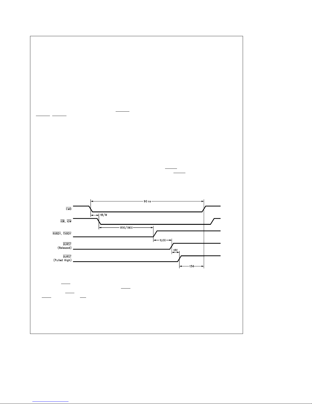
byte transfer. This is the critical timing issue. The timing
diagram in
Figure 1
illustrates the signals and delays in-
volved.
Timing Parameters:
tR/W: Time to decode S0, S1 and M/IO signals into IOR and IOW strobes.
tRXI/tWXI: RXRDYTXRDY
tLOG: Propagation delay of request signal through logic controlling BURST
tRC: RC restoration of BURST
t56: BURST
inactive high setup to CMD inactiveÐMicro Channel specifies 35 ns minimum.
inactive from leading edge of read and write strobes respectively (PC16552C DMA request signal spec).
on the Micro Channel.
TL/F/11195– 2
.
FIGURE 1
8
Page 9

Without extending the bus cycle, the maximum delay time
from the leading edge of CMD
55 ns. The two delays which must be minimized in the DMA
interface design are tR/W and tLOG. tRXI/tWXI are controlled by the PC16552C and tRC is created by the Micro
Channel. It is a quantity that is unknown to this designer as it
is not specified in the IBM Technical Reference Manual.
The PC16552C TXRDY
leased by the rising edge of the last IOW strobe. This makes
it impossible to meet the BURST
therefore perform slave-terminated bursts. The PC16552C
has since been redesigned so that TXRDY
the RXRDY
this package uses DMA controller terminated burst transfers
for the transmitter FIFOs, a method which must be used
with the older revision of the PC16552C. The new revision
of the PC16552C was not available when this documentation was completed. However, slave-terminated transfers
were run with the old revision and the adapter performed
correctly except that due to the lateness of the
BURST
the transmit FIFO. The last byte was lost since the FIFO
was already full. Therefore, the RXTXI.C driver program
should be used with all current PC16552C parts.
A second issue with the PC16552C is the length of both
tRXI and tWXI which are specified as 78 ns and 60 ns
(max). These times plus the delays in the logic implemented
on this adapter forces the use of an extended cycle (wait
state). Using the Synchronous Extended cycle as explained
in the Micro Channel Control Signals section, adds 100 ns
to the length of the CMD
meet the BURST
Adding a wait state is obviously undesirable since it increases the bus cycle length by 50% (200 ns to 300 ns). One way
for a designer to avoid needing a wait state is to minimize
tLOG and tR/W. Besides using fast logic, the delay through
the DMA logic interface can be reduced by implementing
the design with four Local Arbiters. This eliminates the delay
created by the prioritization of the UART requests. Also, an
effort is being made to reduce the tRXI and tWXI specs on
the PC16552C. Finally, the IBM documentation is not clear
as to whether the t56 spec must be met for both IO read/
memory write and memory read/IO write transfers. The
spec is marked on the timing diagrams for both types of
transfers, but a separate note says that the spec must be
guaranteed for IO write cycles with no mention of the IO
read cycles. It is likely that the spec need not be met for IO
read cycles because the read to the IO device occurs long
before the end of the byte transfer since the byte must still
be written to memory.
While it did not meet worst-case specifications, the
PC16552C Adapter (with the old PC16552C rev) was also
tested without a wait state and ran I/O read DMA transfers
without errors. A test of the IO write transfers was futile
because only the older PC16552C was available making
slave-terminated transfers impossible.
The design chosen for implementation uses just one Local
Arbiter and prioritizes the UART DMA requests on the
adapter. This design was chosen because it is more inform-
signals. The RXTXI.C driver program included in
deassertion, a 17th byte was always transferred to
signals were designed to be re-
strobe, providing enough time to
inactive specification.
to BURST inactive is
inactive setup time and
is released by
ative example and has a lower chip count. This section describes the following functions of the interface logic: enable/disable of UART DMA requests; prioritization of the
four DMA requests; selection of the proper arbitration vector; local bus arbitration; fairness and Terminal Count interrupt generation. Refer to the block diagram and schematics
for the PC16552C Adapter during the following discussions.
DMA Request Enable
A 4-bit write-only DMA request enable/disable register
(DMAÐEN) is implemented on the PC16552C Adapter using four 74LS74 latches. The complemented outputs of the
latches are used to gate the PC16552C’s DMA request signals RXRDY
the system CPU must writea1tothebitlocations corresponding to those requests. Table I summarizes the register’s function.
76543210
X X X X 0 0 0 0 All DMA Request Disabled
X X X X 0 0 0 1 TXRDY2
X X X X 0 0 1 0 TXRDY1
X X X X 0 1 0 0 RXRDY2
X X X X 1 0 0 0 RXRDY1 Enabled
DMAÐEN is necessary to prevent errant DMA requests to
the Micro Channel (such as the immediate transmitter requests after reset) and to maintain compatibility with standard CPU-serviced serial port operation. A hardware disable
is also implemented and is described in the TC Interrupt
section.
DMAÐEN is located at I/O address 2F7h. This location is
not used by IBM and was chosen because of its similarity to
the COM2 address block made the decode simpler. The
active low output of the register’s address decoder is gated
with the IOW signal to produce a write strobe to the CLK
inputs of the 74LS74 latches.
DMA Request Prioritization
If the adapter card is used at its full capability i.e. four simultaneous DMA-serviced file transfers, the four UART DMA
request strobes will operate as fully independent, asynchronous signals. The asynchronous state machine, Lockout,
implemented in a 16L8D GAL, is used to select the highest
priority active DMA request and lock out all other requests
until that request has been serviced. The state diagram for
Lockout is illustrated in
in the Idle state until one or more DMA requests go active.
The requests are the active high gated versions of the
RXRDY
and TX2. An active request moves Lockout to the corresponding request state. If more than one request are active
at once, the machine will move to the highest priority state.
The requests are prioritized as follows: RX1 (highest), RX2,
TX1 and TX2. Note that this prioritization mechanism provides adapter-level arbitration between the requests leaving
only one which competes for the bus at the system level
(Central Arbitration).
and TXRDY. To enable DMA request signals,
TABLE I
DMAÐEN Bits
Enabled
Enabled
Enabled
Figure 2
. The state machine resides
and TXRDY signals and are called RX1, TX1, RX2,
9
Page 10

FIGURE 2. Lockout State Machine
Upon entering a request state, Lockout asserts the DREQ
signal and a 2-bit code, S1 and S0 (not to be confused with
the bus signals S1, S0) corresponding to the request selected. The machine remains in the request state until the corresponding request signal goes inactive signifying the end
of the DMA service. It then moves back to the idle state,
deasserts DREQ
and waits for a new request.
A delay feature was implemented to handle two or more
requests active at one time. Without this delay, the machine
would move very quickly from a request state, through the
Idle state and into the next highest priority request state.
The result is that the DREQ
signal, which is inactive only
while in the Idle state, does not go inactive long enough to
cause a state change in the Busarb state machine (see Local Arbiter). BUSARB must change states so that it can signal the end of a transfer to the DMA controller by deasserting BURST
feedback DREQ
a transfer, DREQ
. The Delay input to the Lockout machine is the
signal, inverted and delayed 100 ns. During
is active low and the Delay signal is active
high. At the end of a transfer cycle, the Lockout machine
moves to the Idle state and deaserts DREQ
. It will stay in
Idle until the Delay signal goes inactive low 100 ns later.
Thus DREQ
is guaranteed to be inactive for at least 100 ns.
TL/F/11195– 3
Selection of Arbitration Vector
The PC16552C Adapter is designed to store four different
arbitration vectors which correspond to the 4 DMA channels
programmed to service the UART’s RXRDY
and TXRDY
DMA request signals. Two 74LS153 Dual 4-Line to 1-Line
Data selectors are used to present the proper vector to the
Arbcon PAL for arbitration (see Local Arbiter). The S0, S1
outputs of Lockout are connected to the select inputs of the
Data Selectors. The data inputs to the selectors are the
outputs of the POS registers holding the arbitration vectors.
Note, however, that in this design the vector for TXRDY1
hardwired to 0111, the lowest priority vector, due to lack of
POS space. Another POS register could have been added
to provide flexibility for the TXRDY1
vector, but would have
required additional logic.
Local Arbiter
The PC16552C Adapter implements the Local Arbiter in two
PALs, Arbcon and Busarb.
The Arbcon 20L8A PAL implements the vector arbitration
function. It competes for the bus with the vector belonging
to the UART request selected by Lockout. The ENARB signal from the Busarb state machine gates the vector onto the
ARB bus during the arbitration cycle. If the Arbcon logic
finds a match between its vector and the ARB bus, it has
won the bus and signals to the Busarb machine by asserting
BUSWIN
.
is
10
Page 11

FIGURE 3. Busarb State Machine
An asynchronous state machine, Busarb, implemented in a
20V8D GAL, controls the bus arbitration. It connects directly
to the ARB/GNT, PREEMPT
, BURST and CHRESET Micro
Channel signals. The following describes Busarb’s states
and operation.
Figure 3
illustrates the state diagram.
IDLE: No DMA requests from UART (DREQe1).
REQ: UART is requesting DMA service. PREEMPT
is as-
serted to request control of the bus.
ARB: Central Arbiter has begun arbitration cycle. ENARB
is asserted causing Arbcon to start competing for
the bus. PREEMPT
still active.
LOSE: Central Arbiter ends arbitration cycle. Arbcon did not
win vector arbitration so BUSWIN was not asserted.
ENARB is deasserted causing Arbcon to degate its
vector. PREEMPT remains active. When the winning
device is finished, the Central Arbiter will start a new
arbitration cycle and Busarb will move back into the
ARB state.
XFR1: The PC16552C Adapter has won arbitration. This is
an intermediate state to XFR2 needed to prevent
more than one bit from changing between states.
The state transitions from intermediate states
(XFR1 and XFR2) are unconditional and marked
‘‘uct’’ on the state diagram. PREEMPT
deasserted.
XFR2: BURST is asserted and DMA controller begins
transfer.
XFR3: DREQ
has gone inactive signifying completion of
transfer. BURST
is deasserted. This is an intermedi-
ate state to IDLE.
TL/F/11195– 4
Fairness
IBM’s Fairness algorithm is enabled when POS register 102
bit 7 is set. An asynchronous state machine for each of the
four UART DMA request signals, implemented in 2 PALs,
Fair1 and Fair2, ensures that the four requests obey the
Fairness algorithm by disabling them when Fairness requires them to wait.
All four machines have the same 7 inputs: CHRESET, FAIR,
PREEMPT
and the four gated UART requests: RX1, RX2,
TX1 and TX2. The machines have one unique output, FR,
that is a second UART request gating signal along with the
DMAÐEN output. The Fairness state machines have the
following states:
[
1,1]IDLE: Reset state. Particular DMA request (RX1,
TX1, RX2, TX2) not active. Output: none.
[
1,0]XFR: DMA request active. Output: none.
[
0,0]FAIR: DMA request goes inactive, FAIR
e
1 (enabled) and at least one other UART request or
PREEMPT
is active. Output: FR degating sig-
nal is active.
[
0,1]TEMP: All requests for bus have gone inactive. This is
an intermediate state to IDLE. Output: FR still
asserted (deasserted upon transition to IDLE).
Figure 4
shows the state diagrams for the RX1 and TX1
state machines. The machines for RX2 and TX2 are identical. On the adapter card, RX1 and RX2 machines are implemented in the 16L8A PAL Fair1 and TX1 and TX2 in Fair2.
11
Page 12

TL/F/11195– 5 TL/F/11195– 6
FIGURE 4. Fairness State Machines
All four machines use their particular DMA request signal
(RX1, RX2, TX1 or TX2) to move from the IDLE state to XFR
to FAIR. But it is all the other request signals that either
keep the machine in the FAIR state (if there is at least one
active) or allow it to move back to IDLE via TEMP (no other
requests active). Thus if a particular channel finishes being
serviced and there are others waiting for service at the time,
the channel will be degated by its FR signal, preventing it
from requesting service again before all other devicesÐ
both UART and other bus devicesÐare finished.
Terminal Count Interrupt
A signal to the CPU that a file or block of data has completed transmission or reception is a crucial feature of a practical DMA-serviced serial port. It is necessary because the
entire transfer process is completely transparent to the
CPU. The CPU must be notified one or all files being transferred are done so that it can start a new transfer, process
received data, notify the user, etc. The DMA controller provides a Terminal Count (TC) pulse when it has transferred
the number of bytes programmed into its Terminal Count
Register (see Software). The PC16552C Adapter uses this
pulse to generate an IRQ3 interrupt and disable the DMA
request line of the UART channel that completed its transfer. The TC signal is common to all devices on the Micro
Channel so it was necessary to decode the signal and create a TC unique to the UART channel that generated it.
Since the DMA controller generates the TC pulse during the
final read or write to the I/O address it is servicing, this was
accomplished by decoding TC along with the adapter’s IOR,
IOW, CS1 and CS2 signals. For example, TC, IOR and CS1
active generates TC pulse unique to the UART’s channel 1
receiver (RXRDY1
The channel-unique TC pulses are connected to the CL
).
inputs of the DMAÐEN register’s 74LS74 latches. The TC
pulse clears the adapter card enable bit for the decoded
channel and prevents any further DMA request from that
channel until the CPU has re-intialized the system for a new
file transfer.
All four UART TC pulses are OR’ed together to set a 1-bit
read-only register called Interrupt Status Register (ISR). The
output of ISR is connected to the INTR GAL and generates
an IRQ3 interrupt (see Adapter Interrupts). ISR was implemented because the Micro Channel requires that adapters
generating interrupts have a status register that the CPU
can poll to determine which adapter caused the interrupt.
The ISR is implemented with two 74LS74 latches connected in a master-slave arrangement. This provides a selfclearing mechanism when the register is read. The register
is located at I/O address 2f7H along with DMAÐEN. Its
read strobe is generated by a logical AND of the 2f7H decoder output and the IOR signal. The read strobe is connected to the clock input of the slave latch and the inverted
strobe is connected to the master’s clock. The strobe is
also connected to the gate input of a 74LS125 buffer which
gates the output of the slave latch onto the Adapter Data
Bus bit 0. The falling edge of the read strobe gates the
register onto the data bus and clears the master latch. The
rising edge clears the slave latch.
SOFTWARE
Programming the Micro Channel DMA Controller
The Micro Channel DMA controller is register and software
compatible with the IBM Personal Computer AT DMA channels, but also has an extended mode of operation. Controller registers can be read and written in the extended mode
using two registers, the Function register and the Execute
Function register. To perform an extended mode register
read/write, the CPU must write to the Function register a 4bit command code in the upper nibble and the channel number in the lower nibble. The command is executed by reading or writing the Execute Function register. The driver programs included in this package illustrate this register access
process.
12
Page 13

The most important feature of the extended mode is that it
provides access to two new registers: the I/O Address register and the Extended Mode register. The programmer can
now use the I/O Address register to specify the address of
the I/O port being serviced (the 8237 and therefore the AT
machines are not capable of generating this address). The
Extended Mode register defines the operation of the channel: Read Memory or Write Memory, Verify or Transfer data,
8-bit or 16-bit transfers and enable/disable of the I/O address generation.
The controller begins the DMA transfers when a DMA slave
has won the arbitration bus and the DMA controller has
been unmasked and programmed to service the winning request. The controller performs transfers serially with separate read and write cycles for each byte or word transferred.
The DMA bus cycles are identical to CPU bus cycles. They
may be Default cycles or be extended by the CHRDY signal.
Driver Programs
Two driver programs are included in this package that demonstrate four simultaneous file transfersÐRXTX.C, which
operates with slave-terminated burst transfers and RXTXI.C,
which uses controller-terminated transfers for the serial
transmitter channels. Both programs are relatively simple
since most of the work is done by the DMA controller, not
the CPU.
RXTX.C
RXTX.C performs the following functions:
Ð allocates 4 RAM buffers the same size as the 4
files being transferred.
Ð initializes the two serial ports to 19.2k, 8, N, 1
and enables the FIFOs and line status registers.
Receiver FIFO trigger levels are set to 14.
Ð programs the following into the DMA controller:
starting address of the RAM buffers into the
#
Memory Address registers
I/O addresses of the UART receive and trans-
#
mit FIFOs into the I/O address registers
number of bytes in the files into the Terminal
#
Count registers
receiver channels’ Extended Mode registers
#
are set for 8-bit transfers from memory to the
programmed I/O addresses
transmit channels’ Extended Mode registers
#
are set for 8-bit transfers from the programmed I/O addresses to memory
Ð fills transmit data buffers with 00 –FFh test data
Ð 8259 PIC is programmed to execute dmaÐint()
upon receiving an IRQ3 interrupt
Ð Enables UART DMA request by writing xFh to
DMAÐEN
Ð waits for all file transfers to complete
The DMA channels programmed for the UART requests are:
channel 0ÐRXRDY1
TXRDY1
; channel 7ÐTXRDY1. These numbers correspond
to the arbitration vectors specified in the adapter’s ADF.
Immediately after enabling the UART DMA requests, the
adapter will generate transmit FIFO empty requests
(TXRDY1
quests and data will begin transmitting from the UART. One
or two other systems must also begin at this time to transmit
and TXRDY2), the controller will service the re-
; channel 1ÐRXRDY1; channel 6Ð
00–FFh test data to the two receivers. The size of these
files must be the same as the Terminal Count programmed
into the DMA channels servicing the receivers. The receivers will generate their first request after the first 14 bytes
arrive. The CPU sits in a wait loop while the DMA controller
continues to service the serial ports. The program stops after all four files have been transferred.
The dmaÐint( ) IRQ3 service routine is executed if a line
status error is generated or a TC is generated by a file transfer completion. The routine first checks for line status errors
in both channels. It then reads the 1-bit Interrupt Status
Register (ISR) which will be set if a TC has occurred. The
program then identifies which of the four file transfers completed by reading the DMA controller’s status registers.
They contain bit locations for all 8 channels which are set if
a TC has been reached on that channel.
For any channel that has generated a TC, the DMA controller mask bit for that channel is set along with a flag signifying file transfer completion. If a channel servicing a receiver
generated a TC, the received data is also verified by checking the data in the RAM buffer. Finally, RAM buffers are
deallocated.
RXTXII.C
This driver is identical to RXTX.C except that the DMA channels servicing the UART transmitter FIFOs are programmed
differently and TC interrupts for the transmitters are serviced differently. This is a sample driver for the old version of
the PC16552C which cannot run slave-terminated bursts on
the transmitter.
The DMA channels for the transmit FIFOs are programmed
with a TC of 16 or lessÐnot with the size of the entire file.
This causes the controller to terminate the burst when the
FIFO is full instead of waiting for TXRDY
which will be late as discussed in Design Considerations.
During initialization and after every burst transfer to the
transmit FIFOs, the TC is programmed for 16 bytes unless
there are less than that left in the file. A software counter
keeps track of the number of bytes transferred.
dmaÐint() is executed after every service of the FIFO because of the TC indication. Line Status interrupts and the
receiver channels are treated the same as in RXTX.C.
Transmitter channels are masked, have their TC registers
reloaded as explained above and then unmasked.
DMAÐEN is written with a special mask variable (chÐcomplete) that remembers which DMA channels are no longer in
operation so as not to inadvertantly enable another channel.
EISA BUS DESIGN COMPARISON
From a DMA slave’s point of view, the DMA system in EISA
machines is essentially the same as in ISA machines. DMA
requests from a slave device interface directly to the EISA
bus DRQ signals. No local arbitration is necessary.
An EISA bus design utilizing the PC16552C DMA request
signals would be much simpler than the Micro Channel design. The RXRDY and TXRDY DMA request signals would
be connected directly to 4 different system DRQ signals,
eliminating the need for the Local Arbiter, Fairness logic,
request selection and lockout, and the generation of 4 arbitration vectors. However it would still be necessary to implement a DMA request enable register and Terminal Count
handling logic.
The advantage of a DMA slave design for an EISA machine
over an ISA machine is the increased DMA transfer rate.
EISA specifies enhanced DMA modes which will transfer
data at a substantially higher rate than the 4 MHz rate that is
standard on ISA machines.
13
to go inactive
Page 14

Adapter Description File ListingÐ@6E6D.adf
Adapterld 06E6Dh
AdapterName ‘‘NSC PC16552C Dual Async Adapter’’
NumBytes 4
NamedItem
Prompt ‘Connector 1‘
choice ‘SERIAL
1‘ pos[0]4X011XXXXb pos[1]4XX000XXXb io 03f8h-03ffh 02f7h-02f7h int 4
choice ‘SERIAL 2‘ pos[0]4X001XXXXb pos[1]4XX000XXXb io 02f8h-02ffh 02f7h-02f7h int 3
choice ‘SERIAL 3‘ pos[0]4X100XXXXb pos[1]4XX011XXXb io 3220h-3227h 02f7h-02f7h int 3
choice ‘SERIAL 4‘ pos[0]4X101XXXXb pos[1]4XX011XXXb io 3228h-322fh 02f7h-02f7h int 3
choice ‘SERIAL
5‘ pos[0]4X100XXXXb pos[1]4XX100XXXb io 4220h-4227h 02f7h-02f7h int 3
choice ‘SERIAL 6‘ pos[0]4X101XXXXb pos[1]4XX100XXXb io 4228h-422fh 02f7h-02f7h int 3
choice ‘SERIAL 7‘ pos[0]4X100XXXXb pos[1]4XX101XXXb io 5220h-5227h 02f7h-02f7h int 3
choice ‘SERIAL 8‘ pos[0]4X101XXXXb pos[1]4XX101XXXb io 5228h-522fh 02f7h-02f7h int 3
Help ‘‘This connector on the IBM Dual Async Adapter can be assigned to use Serial 1 though Serial 8. Use the F5ePrevious
and the F6
e
Next keys to change serial port assignments if you are in the ‘Change configuration’ window. Conflicting assign-
ments are marked with an asterisk and must be changed to use the adapter.’’
NamedItem
Prompt ‘Connector 2‘
choice ‘SERIAL
1‘ pos[0]4XXXX011Xb pos[1]4XXXXX000b io 03f8h-03ffh int 4
choice ‘SERIAL 2‘ pos[0]4XXXX001Xb pos[1]4XXXXX000b io 02f8h-02ffh int 3
choice ‘SERIAL 3‘ pos[0]4XXXX100Xb pos[1]4XXXXX011b io 3220h-3227h int 3
choice ‘SERIAL 4‘ pos[0]4XXXX101Xb pos[1]4XXXXX011b io 3228h-322fh int 3
choice ‘SERIAL
5‘ pos[0]4XXXX100Xb pos[1]4XXXXX100b io 4220h-4227h int 3
choice ‘SERIAL 6‘ pos[0]4XXXX101Xb pos[1]4XXXXX100b io 4228h-422fh int 3
choice ‘SERIAL 7‘ pos[0]4XXXX100Xb pos[1]4XXXXX101b io 5220h-5227h int 3
choice ‘SERIAL 8‘ pos[0]4XXXX101Xb pos[1]4XXXXX101b io 5228h-5227h int 3
Help ‘‘This connector on the IBM Dual Async Adapter can be assigned to use Serial 1 through Serial 8. Use the F5ePrevious
and the F6
e
Next keys to change serial port assignments if you are in the ‘Change configuration’ window. Conflicting assign-
ments are marked with an asterisk and must be changed to use the adapter.’’
NamedItem
Prompt ‘Extended Cycle Mode‘
choice ‘Synchronous Extended‘ pos[3]4XX1XXXXXb
Help ‘‘This sets the synchronous extended mode. It must always be set.’’
NamedItem
Prompt ‘Fairness On/Off‘
choice ‘On‘ pos[0]41XXXXXXXb choice ‘Off‘ pos[0]40XXXXXXXb
Help ‘‘Bus Arbitration Fairness. This controls whether the adapter will release control of the bus when it has been using it
exclusively. All four UART channels will use Fairness when it is On. Under normal circumstances, select
kOnl
.’’
NamedItem
Prompt ‘DMA Arbitration Level for Channel 1 Receiver‘
choice ‘Level 0‘ pos[2]4XXXX0000b arb 0
choice ‘Level 1‘ pos[2]4XXXX0001b arb 1
choice ‘Level 3‘ pos[2]4XXXX0011b arb 3
choice ‘Level 4‘ pos[2]4XXXX0100b arb 4
choice ‘Level 5‘ pos[2]4XXXX0101b arb 5
choice ‘Level 6‘ pos[2]4XXXX0110b arb 6
14
Page 15

Help ‘‘This selects the arbitration level and DMA channel for Channel 1 Receiver.’’
NamedItem
Prompt ‘DMA Arbitration Level for Channel 1 Receiver’
choice ‘Level 0‘ pos[2]40000XXXXb arb 0
choice ‘Level 1‘ pos[2]40001XXXXb arb 1
choice ‘Level 3‘ pos[2]40011XXXXb arb 3
choice ‘Level 4‘ pos[2]40100XXXXb arb 4
choice ‘Level 5‘ pos[2]40101XXXXb arb 5
choice ‘Level 6‘ pos[2]40110XXXXb arb 6
Help ‘‘This selects the arbitration level and DMA channel for Channel 2 Receiver.’’
NamedItem
Prompt ‘DMA Arbitration Level for Channel 1 Transmitter‘
choice ‘Level 0‘ pos[3]4XXXX0000b arb 0
choice ‘Level 1‘ pos[3]4XXXX0001b arb 1
choice ‘Level 3‘ pos[3]4XXXX0011b arb 3
choice ‘Level 4‘ pos[3]4XXXX0100b arb 4
choice ‘Level 5‘ pos[3]4XXXX0101b arb 5
choice ‘Level 6‘ pos[3]4XXXX0110b arb 6
Help ‘‘This selects the arbitration level and DMA channel for Channel 1 Transmitter.’’
PC16552C Adapter PAL/State Machine Equations
BUSARB: Local Arbiter State Machine
The following asynchronous state machine controls the Local Arbiter on the Adapter Card. The device used is a 20L8 PAL.
outputs: q3, q2, q1, q0, burst, preout, ack, enarb: pins 21, 20, 19, 18, 17, 16, 22, 15;
inputs: dreq, arbgnt, buswin, prein, chrst: pins 1, 2, 3, 4, 5;
States of Arbiter
e
[
1,1,1,1];
idle
e
[
1,1,1,0]; ‘‘req uchannel bus; preout (q0) active
req
e
[
arb
1,0,1,0]; ‘‘vector enabled; preout, enarb active
e
[
lose
1,0,0,0]; ‘‘lost arb battle; preout active
e
[
xfer1
0,0,1,0]; ‘‘intermediate state to xfer2
e
[
0,0,1,1]; ‘‘xfering data on bus; burst ack active
xfer2
e
[
xfer3
1,0,1,1]; ‘‘intermediate state to idle
Equations
e
!q0
idle & !dreq & !larbgnt & !chrst # ‘‘This is also PREEMPT
req & !dreq & !arbgnt & !chrst
req & !dreq & arbgnt & !chrst
arb & arbgnt & !chrst
arb & !arbgnt & buswin & !chrst
arb & !arbgnt & !buswin & !chrst
lose & !arbgnt & !chrst
Ý
Ý
Ý
Ý
Ý
Ý
lose & arbgnt & !chrst;
e
arb & !arbgnt & buswin & !chrst
!q1
Ý
lose & !arbgnt & !chrst;
!q2ereq & !dreq & arbgnt & !chrst
arb & arbgnt & !chrst
arb & !arbgnt & buswin & !chrst
arb & !arbgnt & !buswin & !chrst
lose & !arbgnt & !chrst
lose & arbgnt & !chrst
xfer1 & !chrst
Ý
xfer2 & !dreq & !arbgnt & !chrst
Ý
Ý
Ý
Ý
Ý
Ý
Ý
xfer2 & dreq & !arbgnt & !chrst;
15
Page 16

!q3earb & !arbgnt & !buswin & !chrst
Ý
xfer1 & !chrstÝxfer2 & !dreq & !arbgnt & !chrst;
!enarb4arb#xfer1#xfer2; ‘enables arb vector (ARB0-3) on bus
!ack4xfer 2; ‘acknowledge signal enable
burst4xfer2; ‘BURST on MCA Bus (TRI-STATE output)
enable preout4!q0; ‘PREEMPT on MCA Bus (TRI-STATE output)
burst40;
preout40;
ARBCON: Local Arbiter-Arbitration Bus Interface Logic
This logic drives and monitors the 4-bit Arbitration Bus during arbitration cycles. The device used is a 20L10 PAL.
Outputs: buswin, arb3, arb2, arb1, arb0, Q3, Q2, Q; pins 22, 21, 20, 19, 18, 17, 16, 15;
Inputs: sel3, sel2, sel1, sel0, enarb: pins 1, 2, 3, 4, 5;
Equations
e
0; arb2e0; arb1e0; arb0e0; ‘‘When enabled, these TRI-STATE outputs will be pulled low.
arb3
Qe(arb3Ý!sel3);
Q2e(arb3Ý!sel3) & (arb2Ý!sel2);
Q3e(arb1Ý!sel1);
e
!buswin
enable arb3
Q2 & Q3 & (arb0Ý!sel0) and !enarb;
e
!sel3 & !enarb;
enable arb2e!sel2&Q&!enarb;
enable arb1e!sel1 & Q2 & !enarb;
e
enable arb0
!sel0 & Q2 & Q3 & !enarb;
LOCKOUT: Device Request Lockout State Machine
This machine selects and prioritizes the four UART DMA requests and issues a single request to the Local Arbiter. Once a
particular request is selected, all others are locked out. The device used is 16L8D PAL.
Outputs dreq, s1, s0, q0, q1, q2, q3: pins 12, 13, 14, 15, 16, 17, 18;
Inputs: rxrdy1, rxrdy2, txrdy1, txrdy2, delay, chrst: pins 1, 2, 3, 4, 5, 6;
States of lockout machine
idle
e
[
1,1,1,1,]; rx1
e
[
1,1,1,0]; rx2
e
[
1,1,0,1]; tx1
e
[
1,0,1,1,]; tx2
e
[
0,1,1,1];
Equations
e
!q0
idle & rxrdy1 & !delay & !chrstÝ!q0 & rxrdy1 & !chrst;
!q1eidle & !rxrdy1 & rxrdy2 & !delay & !chrstÝq0 & !q1 & rxrdy2 & !chrst;
!q2eidle & !rxrdy1 & !rxrdy2 & txrdy1 & !delay & !chrstÝq0 & q1 & !q2 & txrdy1 & !chrst;
!q3eidle & !rxrdy1 & !rxrdy2 & !txrdy1 & txrdy2 & !delay & !chrstÝq0 & q1 & q2 & !q3 & txrdy2 & !chrst;
e
rx1win
s0
q0; rx2wineq1; tx1wineq2; tx2wineq3;
e
q0 & (!q1Ýq2);
s1eq0 & q1;
dreqerx1win & rx2win & tx1win & tx2win;
16
Page 17

FAIR1/FAIR2: Local Arbiter Fairness State Machines
These equations describe two independent state machines which gate the RXRDY1 and RXRDY2 signals in such a way that
they obey the Fairness algorithm. Both machines are contained in a 16L8 PAL. The equations for the transmitter signal state
machines (contained in FAIR2 PAL) are identical to these equations except that the receiver signals are exchanged for corresponding transmitter signals and vice versa.
Outputs: rx1q1, rx1q0, rx2q1, rx2q0, rx1fair, rx2fair: pins 13, 14, 15, 16, 17, 18;
Inputs: rx1, rx2, tx1, tx2, PREEMPT, fair chrst: pins 1, 2, 3, 4, 5, 6, 7;
States:
rx1Ðst
rx1Ðidle
rx1Ðxfr
rx1Ðwait
rx1Ðtemp
rx2Ðidle
rx2Ðxfr
rx2Ðwait
rx2Ðtemp
e
[
rx1q1, rx1q0]; rx2Ðst
e
e
e
e
e
e
rx1Ðst
rx1Ðst
rx1Ðst
e
rx1Ðst
rx2Ðst
rx2Ðst
rx2Ðst
e
rx2Ðst
ee
ee
ee
ee
ee
ee
ee
ee
[
1,1];
[
1,0];
[
[
1,1];
[
1,0];
[
0,0];
[
0,1];
0,0];
[
0,1];
e
[
rx2q1, rx2q0];
Equations
!rx1q0
e
rx1Ðidle & rx1 & !chrst
rx1Ðxfr & rx1 & !chrst
Ý
Ý
rx1Ðxfr & !rx1 & fair & !chrstÝrx1Ðwait & fair & !(!rx2 & !tx1 & !tx2 & PREEMPT) & !chrst;
!rx1q1erx1Ðxfr & !rx1 & fair & !chrst
rx1Ðwait & !(!rx2 & !tx1 & !tx2 & PREEMPT) & !chrst
Ý
Ý
rx1Ðwait & !rx2 & !tx1 & !tx2 & PREEMPT & !chrst;
!rx2q0erx2Ðdle & rx2 & !chrst
rx2Ðxfr & rx2 & !chrst
rx2Ðxfr & !rx2 & fair !chrst
Ý
Ý
Ý
rx2Ðwait & fair & !(!rx1 & !tx1 & !tx2 & PREEMPT) & !chrst;
!rx2q1
e
rx2Ðxfr & !rx2 & fair & !chrst
rx2Ðwait & !(!rx1 & !tx1 & !tx2 & PREEMPT) & !chrst
Ý
Ý
rx2Ðwait & !rx1 & !tx1 & !tx2 & PREEMPT & !chrst;
rx1faire!rx1q1;
e
rx2fair
!rx2q1;
Interrupt Logic
This logic provides the interface between the UART and TC interrupts and the IRQ3 and IRQ4 signals on the Micro Channel. It
also provides the Adapter ID bytes in response to ID byte reads. The device used is a 16L8 PAL.
Outputs IRQ3ÐEN, IRQ4ÐEN, IRQ3, IRQ4, bit 7, bit 4 bit 1, bit 0: pins 15, 16, 17, 18, 19, 12, 14, 13;
Inputs: intr1, intr2, P102B2, P102B5, CDEN, RD100, RD101, dmaÐint, RDÐBOTH: pins 1, 2, 3, 4, 5, 6, 7, 8, 9;
Equations
enable IRQ3
e
intr1 & !P102B5 & CDEN
intr2 & !P102B2 & CDEN
Ý
Ý
dmaÐint & CDEN;
enable IRQ4eintr1 & P102B5 & CDEN
Ý
intr2 & P102B2 & CDEN;
IRQ3e0; IRQ4e0
enable bit 7
e
RDÐBOTH;
enable bit 4eRDÐBOTH;
enable bit 1e!RD100;
enable bit 0e!RD101;
e
bit 7
0; bit 4e0; bit 1e0; bit 0e0;
17
Page 18

TL/F/11195– 7
18
Page 19

TL/F/11195– 8
19
Page 20

TL/F/11195– 9
20
Page 21

TL/F/11195– 10
21
Page 22

TL/F/11195– 11
22
Page 23

TL/F/11195– 12
23
Page 24

LIFE SUPPORT POLICY
NATIONAL’S PRODUCTS ARE NOT AUTHORIZED FOR USE AS CRITICAL COMPONENTS IN LIFE SUPPORT
DEVICES OR SYSTEMS WITHOUT THE EXPRESS WRITTEN APPROVAL OF THE PRESIDENT OF NATIONAL
SEMICONDUCTOR CORPORATION. As used herein:
1. Life support devices or systems are devices or 2. A critical component is any component of a life
systems which, (a) are intended for surgical implant support device or system whose failure to perform can
into the body, or (b) support or sustain life, and whose be reasonably expected to cause the failure of the life
failure to perform, when properly used in accordance support device or system, or to affect its safety or
with instructions for use provided in the labeling, can effectiveness.
be reasonably expected to result in a significant injury
to the user.
National Semiconductor National Semiconductor National Semiconductor National Semiconductor National Semiconductores National Semiconductor
Corporation GmbH Japan Ltd. Hong Kong Ltd. Do Brazil Ltda. (Australia) Pty, Ltd.
2900 Semiconductor Drive Livry-Gargan-Str. 10 Sumitomo Chemical 13th Floor, Straight Block, Rue Deputado Lacorda Franco Building 16
P.O. Box 58090 D-82256 F4urstenfeldbruck Engineering Center Ocean Centre, 5 Canton Rd. 120-3A Business Park Drive
Santa Clara, CA 95052-8090 Germany Bldg. 7F Tsimshatsui, Kowloon Sao Paulo-SP Monash Business Park
Tel: 1(800) 272-9959 Tel: (81-41) 35-0 1-7-1, Nakase, Mihama-Ku Hong Kong Brazil 05418-000 Nottinghill, Melbourne
TWX: (910) 339-9240 Telex: 527649 Chiba-City, Tel: (852) 2737-1600 Tel: (55-11) 212-5066 Victoria 3168 Australia
AN-770 PC16552C Dual UART/DMA Micro Channel Adapter
National does not assume any responsibilityfor use of any circuitry described, no circuit patent licenses are impliedand National reserves the right at any time without notice tochange said circuitry and specifications.
Fax: (81-41) 35-1 Ciba Prefecture 261 Fax: (852) 2736-9960 Telex: 391-1131931 NSBR BR Tel: (3) 558-9999
Tel: (043) 299-2300 Fax: (55-11) 212-1181 Fax: (3) 558-9998
Fax: (043) 299-2500
 Loading...