

Page 1
NS32081-10/NS32081-15 Floating-Point Units
NS32081-10/NS32081-15 Floating-Point Units
July 1988
General Description
The NS32081 Floating-Point Unit functions as a slave processor in National Semiconductor’s Series 32000
É
microprocessor family. It provides a high-speed floating-point instruction set for any Series 32000 family CPU, while remaining architecturally consistent with the full two-address architecture and powerful addressing modes of the Series 32000
micro-processor family.
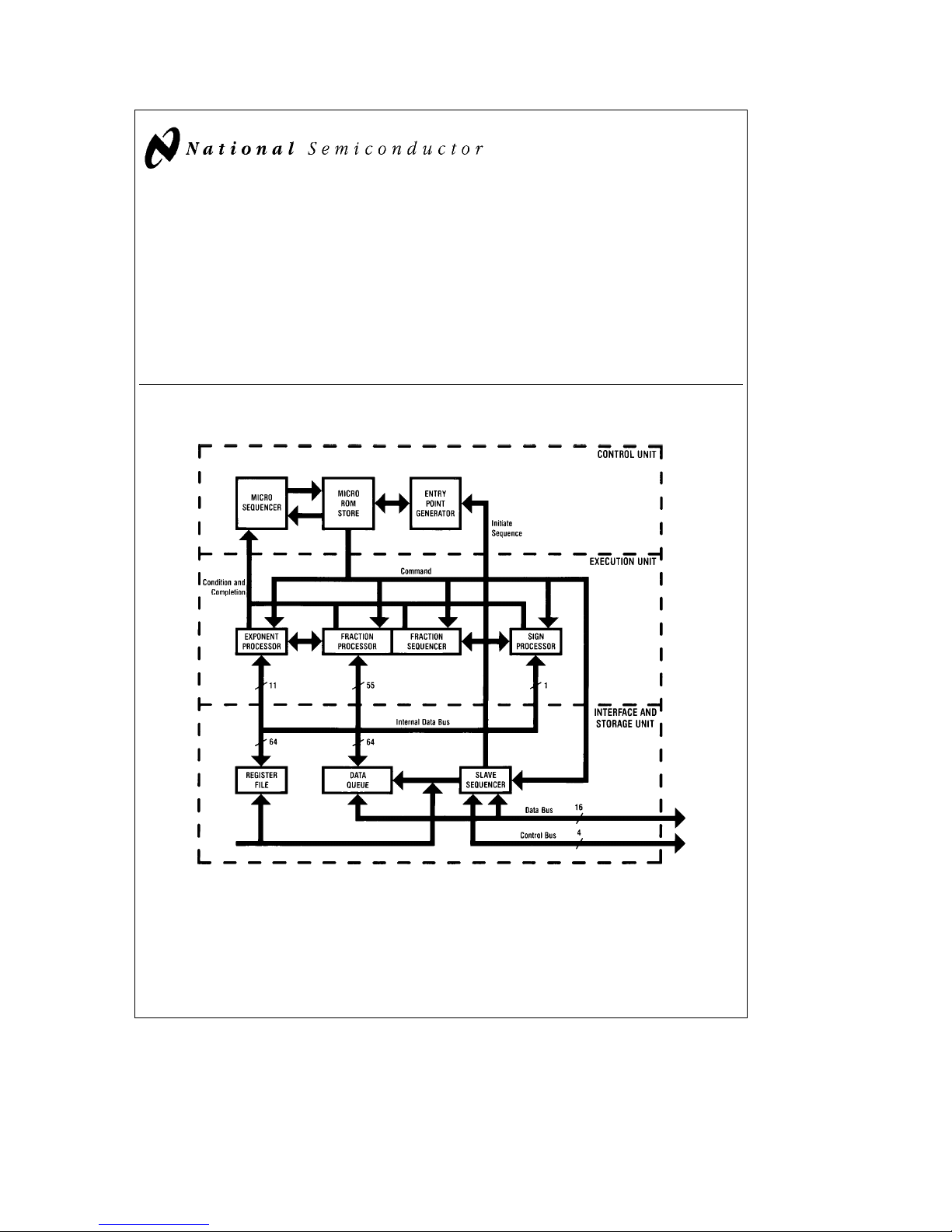
Block Diagram
Features
Y
Eight on-chip data registers
Y
32-bit and 64-bit operations
Y
Supports proposed IEEE standard for binary floatingpoint arithmetic, Task P754
Y
Directly compatible with NS32016, NS32008 and
NS32032 CPUs
Y
High-speed XMOSTMtechnology
Y
Single 5V supply
Y
24-pin dual in-line package
TRI-STATEÉand Series 32000Éare registered trademarks of National Semiconductor Corp.
TM
XMOS
is a trademark of National Semiconductor Corp.
C
1995 National Semiconductor Corporation RRD-B30M105/Printed in U. S. A.
TL/EE/5234
TL/EE/5234– 1
Page 2

Table of Contents
1.0 PRODUCT INTRODUCTION
1.1 Operand Formats
1.1.1 Normalized Numbers
1.1.2 Zero
1.1.3 Reserved Operands
1.1.4 Integers
1.1.5 Memory Representations
2.0 ARCHITECTURAL DESCRIPTION
2.1 Programming Model
2.1.1 Floating-Point Registers
2.1.2 Floating-Point Status Register (FSR)
2.1.2.1 FSR Mode Control Fields
2.1.2.2 FSR Status Fields
2.1.2.3 FSR Software Field (SWF)
2.2 Instruction Set
2.2.1 General Instruction Format
2.2.2 Addressing Modes
2.2.3 Floating-Point Instruction Set
2.3 Traps
3.0 FUNCTIONAL DESCRIPTION
3.1 Power and Grounding
3.2 Clocking
3.3 Resetting
3.0 FUNCTIONAL DESCRIPTION (Continued)
3.4 Bus Operation
3.4.1 Bus Cycles
3.4.2 Operand Transfer Sequences
3.5 Instruction Protocols
3.5.1 General Protocol Sequence
3.5.2 Floating-Point Protocols
4.0 DEVICE SPECIFICATIONS
4.1 Pin Descriptions
4.1.1 Supplies
4.1.2 Input Signals
4.1.3 Input/Output Signals
4.2 Absolute Maximum Ratings
4.3 Electrical Characteristics
4.4 Switching Characteristics
4.4.1 Definitions
4.4.2 Timing Tables
4.4.2.1 Output Signals: Internal Propagation Delays
4.4.2.2 Input Signals Requirements
4.4.2.3 Clocking Requirements
4.4.3 Timing Diagrams
2
Page 3

List of Illustrations
Floating-Point Operand Formats ААААААААААААААААААААААААААААААААААААААААААААААААААААААААААААААААААААААААААААААААА1-1
Register Set ААААААААААААААААААААААААААААААААААААААААААААААААААААААААААААААААААААААААААААААААААААААААААААААААААА2-1
The Floating-Point Status Register ААААААААААААААААААААААААААААААААААААААААААААААААААААААААААААААААААААААААААААААА2-2
General Instruction Format АААААААААААААААААААААААААААААААААААААААААААААААААААААААААААААААААААААААААААААААААААААА2-3
Index Byte Format ААААААААААААААААААААААААААААААААААААААААААААААААААААААААААААААААААААААААААААААААААААААААААААА2-4
Displacement EncodingsАААААААААААААААААААААААААААААААААААААААААААААААААААААААААААААААААААААААААААААААААААААААА2-5
Floating-Point Instruction FormatsАААААААААААААААААААААААААААААААААААААААААААААААААААААААААААААААААААААААААААААААА2-6
Recommended Supply Connections АААААААААААААААААААААААААААААААААААААААААААААААААААААААААААААААААААААААААААААА3-1
Power-On Reset Requirements АААААААААААААААААААААААААААААААААААААААААААААААААААААААААААААААААААААААААААААААААА3-2
General Reset Timing АААААААААААААААААААААААААААААААААААААААААААААААААААААААААААААААААААААААААААААААААААААААААА3-3
System Connection Diagram АААААААААААААААААААААААААААААААААААААААААААААААААААААААААААААААААААААААААААААААААААА3-4
Slave Processor Read CycleААААААААААААААААААААААААААААААААААААААААААААААААААААААААААААААААААААААААААААААААААААА3-5
Slave Processor Write CycleААААААААААААААААААААААААААААААААААААААААААААААААААААААААААААААААААААААААААААААААААААА3-6
FPU Protocol Status Word FormatАААААААААААААААААААААААААААААААААААААААААААААААААААААААААААААААААААААААААААААААА3-7
Dual-In-Line PackageААААААААААААААААААААААААААААААААААААААААААААААААААААААААААААААААААААААААААААААААААААААААААА4-1
Timing Specification Standard (Signal Valid After Clock Edge)АААААААААААААААААААААААААААААААААААААААААААААААААААААААА4-2
Timing Specification Standard (Signal Valid Before Clock Edge) АААААААААААААААААААААААААААААААААААААААААААААААААААААА4-3
Clock Timing АААААААААААААААААААААААААААААААААААААААААААААААААААААААААААААААААААААААААААААААААААААААААААААААААА4-4
Power-On-Reset ААААААААААААААААААААААААААААААААААААААААААААААААААААААААААААААААААААААААААААААААААААААААААААААА4-5
Non-Power-On-ResetААААААААААААААААААААААААААААААААААААААААААААААААААААААААААААААААААААААААААААААААААААААААААА4-6
Read Cycle From FPU АААААААААААААААААААААААААААААААААААААААААААААААААААААААААААААААААААААААААААААААААААААААААА4-7
Write Cycle To FPU АААААААААААААААААААААААААААААААААААААААААААААААААААААААААААААААААААААААААААААААААААААААААААА4-8
Pulse from FPU ААААААААААААААААААААААААААААААААААААААААААААААААААААААААААААААААААААААААААААААААААААААААААА4-9
SPC
RST Release Timing АААААААААААААААААААААААААААААААААААААААААААААААААААААААААААААААААААААААААААААААААААААААААА4-10
List of Tables
Sample F Fields ААААААААААААААААААААААААААААААААААААААААААААААААААААААААААААААААААААААААААААААААААААААААААААААА1-1
Sample E Fields ААААААААААААААААААААААААААААААААААААААААААААААААААААААААААААААААААААААААААААААААААААААААААААААА1-2
Normalized Number RangesААААААААААААААААААААААААААААААААААААААААААААААААААААААААААААААААААААААААААААААААААААА1-3
Series 32000 Family Addressing ModesААААААААААААААААААААААААААААААААААААААААААААААААААААААААААААААААААААААААААА2-1
General Instruction Protocol ААААААААААААААААААААААААААААААААААААААААААААААААААААААААААААААААААААААААААААААААААААА3-1
Floating-Point Instruction ProtocolsААААААААААААААААААААААААААААААААААААААААААААААААААААААААААААААААААААААААААААААА3-2
3
Page 4

1.0 Product Introduction
The NS32081 Floating-Point Unit (FPU) provides high
speed floating-point operations for the Series 32000 family,
and is fabricated using National high-speed XMOS technology. It operates as a slave processor for transparent expansion of the Series 32000 CPU’s basic instruction set. The
FPU can also be used with other microprocessors as a peripheral device by using additional TTL interface logic. The
NS32081 is compatible with the IEEE Floating-Point Formats by means of its hardware and software features.
1.1 OPERAND FORMATS
The NS32081 FPU operates on two floating-point data
typesÐsingle precision (32 bits) and double precision (64
bits). Floating-point instruction mnemonics use the suffix F
(Floating) to select the single precision data type, and the
suffix L (Long Floating) to select the double precision data
type.
A floating-point number is divided into three fields, as shown
in
Figure 1-1
.
The F field is the fractional portion of the represented number. In Normalized numbers (Section 1.1.1), the binary point
is assumed to be immediately to the left of the most significant bit of the F field, with an implied 1 bit to the left of the
binary point. Thus, the F field represents values in the range
sxs
1.0
2.0.
TABLE 1-1. Sample F Fields
F Field Binary Value Decimal Value
000...0 1.000...0 1.000...0
010...0 1.010...0 1.250...0
100...0 1.100...0 1.500...0
110...0 1.110...0 1.750...0
u
Implied Bit
The E field contains an unsigned number that gives the binary exponent of the represented number. The value in the
E field is biased; that is, a constant bias value must be subtracted from the E field value in order to obtain the true
exponent. The bias value is 011...11
(single precision) or 1023 (double precision). Thus, the true
exponent can be either positive or negative, as shown in
Table 1-2.
, which is either 127
2
TABLE 1-2. Sample E Fields
E Field F Field Represented Value
011...110 100...0 1.5
011...111 100...0 1.5
100...000 100...0 1.5
b
1
c
e
2
0.75
0
c
e
2
1.50
1
c
e
2
3.00
Two values of the E field are not exponents. 11...11 signals a reserved operand (Section 2.1.3). 00...00 represents the number zero if the F field is also all zeroes, otherwise it signals a reserved operand.
The S bit indicates the sign of the operand. It is 0 for positive and 1 for negative. Floating-point numbers are in signmagnitude form, that is, only the S bit is complemented in
order to change the sign of the represented number.
1.1.1 Normalized Numbers
Normalized numbers are numbers which can be expressed
as floating-point operands, as described above, where the E
field is neither all zeroes nor all ones.
The value of a Normalized number can be derived by the
formula:
S
(E-Bias)
c
b
(
1)
c
2
(1aF)
The range of Normalized numbers is given in Table 1-3.
1.1.2 Zero
There are two representations for zeroÐpositive and negative. Positive zero has all-zero F and E fields, and the S bit is
zero. Negative zero also has all-zero F and E fields, but its S
bit is one.
1.1.3 Reserved Operands
The proposed IEEE Standard for Binary Floating-Point Arithmetic (Task P754) provides for certain exceptional forms of
floating-point operands. The NS32081 FPU treats these
forms as reserved operands. The reserved operands are:
Positive and negative infinity
#
Not-a-Number (NaN) values
#
Denormalized numbers
#
Both Infinity and NaN values have all ones in their E fields.
Denormalized numbers have all zeroes in their E fields and
non-zero values in their F fields.
The NS32081 FPU causes an Invalid Operation trap (Section 2.1.2.2) if it receives a reserved operand, unless the
operation is simply a move (without conversion). The FPU
does not generate reserved operands as results.
63 62 52 51 0
SE F
111 52
FIGURE 1-1. Floating-Point Operand Formats
Single Precision
31 30 23 22 0
SE F
18 23
Double Precision
4
Page 5
1.0 Product Introduction (Continued)
TABLE 1-3. Normalized Number Ranges
Single Precision Double Precision
Most Positive 2
Least Positive 2
Least Negative
Most Negative
Note: The values given are extended one full digit beyond their represented accuracy to help in generating rounding and conversion algorithms.
127
e
3.40282346c10
b
e
1.17549436c10
b
(2
eb
b
2
eb
1.1.4 Integers
In addition to performing floating-point arithmetic, the
NS32081 FPU performs conversions between integer and
floating-point data types. Integers are accepted or generated by the FPU as two’s complement values of byte (8 bits),
word (16 bits) or double word (32 bits) length.
1.1.5 Memory Representations
The NS32081 FPU does not directly access memory. However, it is cooperatively involved in the execution of a set of
two-address instructions with its Series 32000 Family CPU.
The CPU determines the representation of operands in
memory.
In the Series 32000 family of CPUs, operands are stored in
memory with the least significant byte at the lowest byte
address. The only exception to this rule is the Immediate
addressing mode, where the operand is held (within the instruction format) with the most significant byte at the lowest
address.
2.0 Architectural Description
b
23
c
(2b2
126
b
126
)
1.17549436c10
c
(2b2
b
127
3.40282346c10
)2
38
b
38
b
38
23
)
38
1023
e
1.7976931348623157c10
b
1022
2
e
2.2250738585072014c10
b
(2
eb
1023
b
2
eb
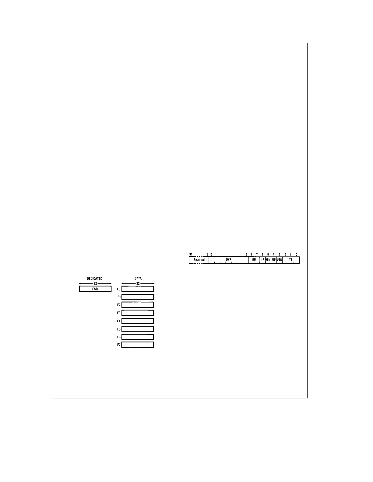
2.1.1 Floating-Point Registers
There are eight registers (F0–F7) on the NS32081 FPU for
providing high-speed access to floating-point operands.
Each is 32 bits long. A floating-point register is referenced
whenever a floating-point instruction uses the Register addressing mode (Section 2.2.2) for a floating-point operand.
All other Register mode usages (i.e., integer operands) refer
to the General Purpose Registers (R0 –R7) of the CPU, and
the FPU transfers the operand as if it were in memory.
When the Register addressing mode is specified for a double precision (64-bit) operand, a pair of registers holds the
operand. The programmer must specify the even register of
the pair. The even register contains the least significant half
of the operand and the next consecutive register contains
the most significant half.
2.1.2 Floating-Point Status Register (FSR)
The Floating-Point Status Register (FSR) selects operating
modes and records any exceptional conditions encountered
during execution of a floating-point operation.
shows the format of the FSR.
2.1 PROGRAMMING MODEL
The Series 32000 architecture includes nine registers that
are implemented on the NS32081 Floating-Point Unit (FPU).
FIGURE 2-2. The Floating-Point Status Register
2.1.2.1 FSR Mode Control Fields
The FSR mode control fields select FPU operation modes.
The meanings of the FSR mode control bits are given below.
Rounding Mode (RM): Bits 7 and 8. This field selects the
rounding method. Floating-point results are rounded whenever they cannot be exactly represented. The rounding
modes are:
00 Round to nearest value. The value which is nearest to
the exact result is returned. If the result is exactly halfway between the two nearest values the even value
e
(LSB
0) is returned.
FIGURE 2-1. Register Set
TL/EE/5234– 4
01 Round toward zero. The nearest value which is closer to
zero or equal to the exact result is returned.
b
52
c
(2b2
b
1022
)
)
2.2250738585072014c10
b
(2b2
52
)
c
1.7976931348623157c10
308
b
308
b
308
308
Figure 2-2
TL/EE/5234– 5
5
Page 6
2.0 Architectural Description (Continued)
10 Round toward positive infinity. The nearest value which
is greater than or equal to the exact result is returned.
11 Round toward negative infinity. The nearest value which
is less than or equal to the exact result is returned.
Underflow Trap Enable (UEN): Bit 3. If this bit is set, the
FPU requests a trap whenever a result is too small in absolute value to be represented as a normalized number. If it is
not set, any underflow condition returns a result of exactly
zero.
Inexact Result Trap Enable (IEN): Bit 5. If this bit is set,
the FPU requests a trap whenever the result of an operation
cannot be represented exactly in the operand format of the
destination. If it is not set, the result is rounded according to
the selected rounding mode.
2.1.2.2 FSR Status Fields
The FSR Status Fields record exceptional conditions encountered during floating-point data processing. The meanings of the FSR status bits are given below:
Trap Type (TT): bits 0-2. This 3-bit field records any exceptional condition detected by a floating-point instruction. The
TT field is loaded with zero whenever any floating-point instruction except LFSR or SFSR completes without encountering an exceptional condition. It is also set to zero by a
hardware reset or by writing zero into it with the Load FSR
(LFSR) instruction. Underflow and Inexact Result are always
reported in the TT field, regardless of the settings of the
UEN and IEN bits.
000 No exceptional condition occurred.
001 Underflow. A non-zero floating-point result is too small
in magnitude to be represented as a normalized floating-point number in the format of the destination operand. This condition is always reported in the TT field
and UF bit, but causes a trap only if the UEN bit is set. If
the UEN bit is not set, a result of Positive Zero is produced, and no trap occurs.
010 Overflow. A result (either floating-point or integer) of a
floating-point instruction is too great in magnitude to be
held in the format of the destination operand. Note that
rounding, as well as calculations, can cause this condition.
011 Divide by zero. An attempt has been made to divide a
non-zero floating-point number by zero. Dividing zero by
zero is considered an Invalid Operation instead (below).
100 Illegal Instruction. Two undefined floating-point instruc-
tion forms are detected by the FPU as being illegal. The
binary formats causing this trap are:
xxxxxxxxxx0011xx10111110
xxxxxxxxxx1001xx10111110
101 Invalid Operation. One of the floating-point operands of
a floating-point instruction is a Reserved operand, or an
attempt has been made to divide zero by zero using the
DIVf instruction.
110 Inexact Result. The result (either floating-point or inte-
ger) of a floating-point instruction cannot be represented exactly in the format of the destination operand, and
a rounding step must alter it to fit. This condition is always reported in the TT field and IF bit unless any other
exceptional condition has occurred in the same instruction. In this case, the TT field always contains the code
for the other exception and the IF bit is not altered. A
trap is caused by this condition only if the IEN bit is set;
otherwise the result is rounded and delivered, and no
trap occurs.
111 (Reserved for future use.)
Underflow Flag (UF): Bit 4. This bit is set by the FPU whenever a result is too small in absolute value to be represented
as a normalized number. Its function is not affected by the
state of the UEN bit. The UF bit is cleared only by writing a
zero into it with the Load FSR instruction or by a hardware
reset.
Inexact Result Flag (IF): Bit 6. This bit is set by the FPU
whenever the result of an operation must be rounded to fit
within the destination format. The IF bit is set only if no other
error has occurred. It is cleared only by writing a zero into it
with the Load FSR instruction or by a hardware reset.
2.1.2.3 FSR Software Field (SWF)
Bits 9-15 of the FSR hold and display any information written to them (using the LFSR and SFSR instructions), but are
not otherwise used by FPU hardware. They are reserved for
use with NSC floating-point extension software.
2.2 INSTRUCTION SET
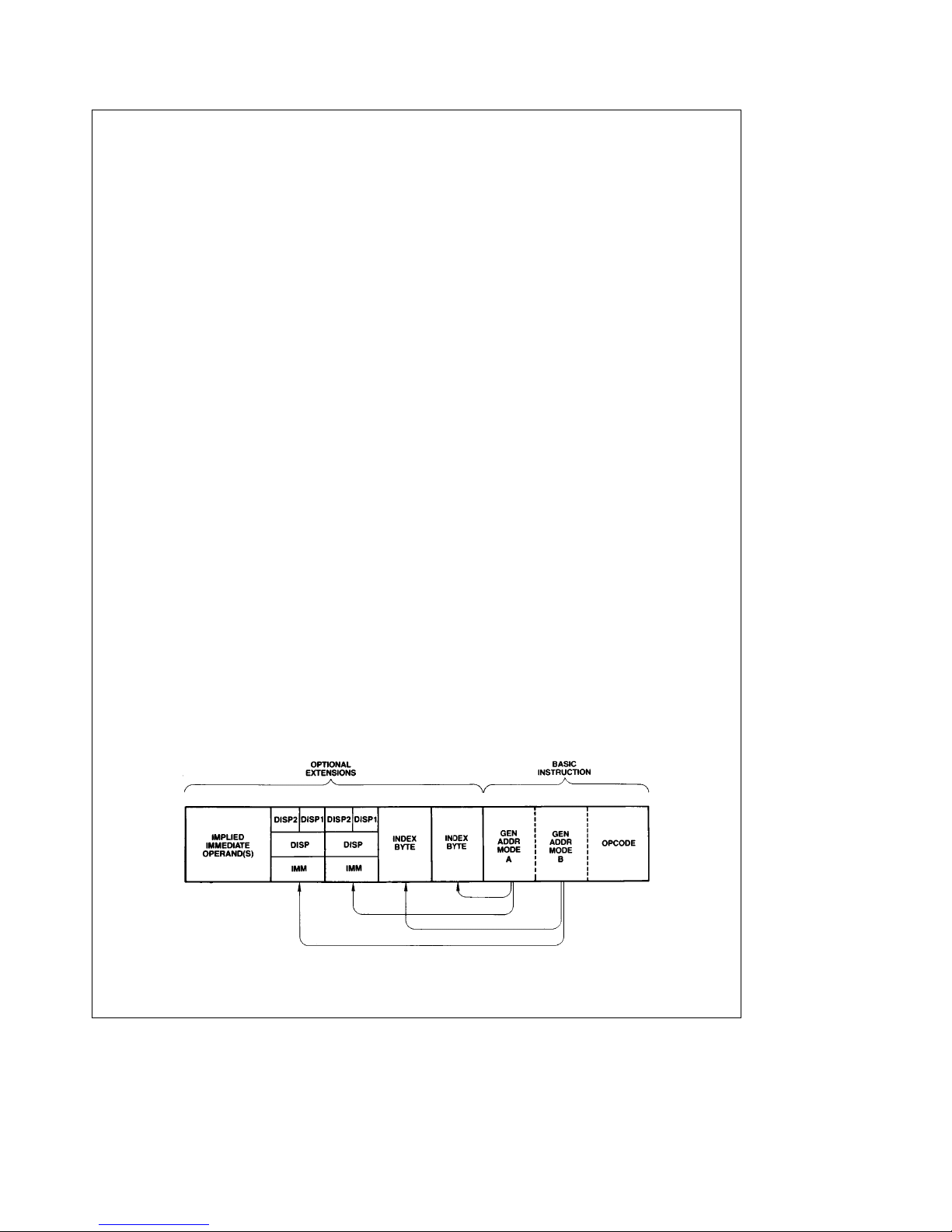
2.2.1 General Instruction Format
Figure 2-3
instruction. The Basic Instruction is one to three bytes long
shows the general format of an Series 32000
FIGURE 2-3. General Instruction Format
TL/EE/5234– 6
6
Page 7

2.0 Architectural Description (Continued)
and contains the opcode and up to two 5-bit General Addressing Mode (Gen) fields. Following the Basic Instruction
field is a set of optional extensions, which may appear depending on the instruction and the addressing modes selected.
The only form of extension issued to the NS32081 FPU is
an Immediate operand. Other extensions are used only by
the CPU to reference memory operands needed by the
FPU.
Index Bytes appear when either or both Gen fields specify
Scaled Index. In this case, the Gen field specifies only the
Scale Factor (1, 2, 4 or 8), and the Index Byte specifies
which General Purpose Register to use as the index, and
which addressing mode calculation to perform before indexing. See
Figure 2-4
Following Index Bytes come any displacements (addressing
constants) or immediate values associated with the selected addressing modes. Each Disp/lmm field may contain
one or two displacements, or one immediate value. The size
of a Displacement field is encoded within the top bits of that
field, as shown in
preted as a signed (two’s complement) value. The size of an
immediate value is determined from the Opcode field. Both
Displacement and Immediate fields are stored most significant byte first.
Some non-FPU instructions require additional, ‘‘implied’’ immediates and/or displacements, apart from those associated with addressing modes. Any such extensions appear at
the end of the instruction, in the order that they appear within the list of operands in the instruction definition.
2.2.2 Addressing Modes
The Series 32000 Family CPUs generally access an operand by calculating its Effective Address based on information available when the operand is to be accessed. The
method to be used in performing this calculation is specified
by the programmer as an ‘‘addressing mode.’’
Addressing modes in the Series 32000 family are designed
to optimally support high-level language accesses to variables. In nearly all cases, a variable access requires only
one addressing mode within the instruction which acts upon
that variable. Extraneous data movement is therefore minimized.
Series 32000 Addressing Modes fall into nine basic types:
Register: In floating-point instructions, these addressing
modes refer to a Floating-Point Register (F0 –F7) if the operand is of a floating-point type. Otherwise, a CPU General
Purpose Register (R0 –R7) is referenced. See Section 2.1.1.
Register Relative: A CPU General Purpose Register contains an address to which is added a displacement value
from the instruction, yielding the Effective Address of the
operand in memory.
.
Figure 2-5
, with the remaining bits inter-
Memory Space: Identical to Register Relative above, except that the register used is one of the dedicated CPU
registers PC, SP, SB or FP. These registers point to data
areas generally needed by high-level languages.
Memory Relative: A pointer variable is found within the
memory space pointed to by the CPU SP, SB or FP register.
A displacement is added to that pointer to generate the Effective Address of the operand.
Immediate: The operand is encoded within the instruction.
This addressing mode is not allowed if the operand is to be
written. Floating-point operands as well as integer operands
may be specified using Immediate mode.
Absolute: The address of the operand is specified by a
Displacement field in the instruction.
External: A pointer value is read from a specified entry of
the current Link Table. To this pointer value is added a displacement, yielding the Effective Address of the operand.
Top of Stack: The currently-selected CPU Stack Pointer
(SP0 or SP1) specifies the location of the operand. The operand is pushed or popped, depending on whether it is written or read.
Scaled Index: Although encoded as an addressing mode,
Scaled Indexing is an option on any addressing mode except Immediate or another Scaled Index. It has the effect of
calculating an Effective Address, then multiplying any General Purpose Register by 1, 2, 4 or 8 and adding it into the
total, yielding the final Effective Address of the operand.
The following table, Table 2-1, is a brief summary of the
addressing modes. For a complete description of their actions, see the Series 32000 Instruction Set Reference Manual.
TL/EE/5234– 10
FIGURE 2-5. Displacement Encodings
FIGURE 2-4. Index Byte Format
TL/EE/5234– 7
7
Page 8

2.0 Architectural Description (Continued)
TABLE 2-1. Series 32000 Family Addressing Modes
Encoding Mode Assembler Syntax Effective Address
REGISTER
00000 Register 0 R0 or F0 None: Operand is in the specified register.
00001 Register 1 R1 or F1
00010 Register 2 R2 or F2
00011 Register 3 R3 or F3
00100 Register 4 R4 or F4
00101 Register 5 R5 or F5
00110 Register 6 R6 or F6
00111 Register 7 R7 or F7
REGISTER RELATIVE
01000 Register 0 relative disp(R0) Disp
01001 Register 1 relative disp(R1)
01010 Register 2 relative disp(R2)
01011 Register 3 relative disp(R3)
01100 Register 4 relative disp(R4)
01101 Register 5 relative disp(R5)
01110 Register 6 relative disp(R6)
01111 Register 7 relative disp(R7)
MEMORY SPACE
11000 Frame memory disp(FP) Disp
11001 Stack memory disp(SP) SP0 or SP1, as selected in PSR.
11010 Static memory disp(SB)
11011 Program memory *
a
disp
MEMORY RELATIVE
10000 Frame memory relative disp2(disp1(FP)) Disp2
10001 Stack memory relative disp2(disp1(SP)) address Disp1
10010 Static memory relative disp2(disp1(SB)) either SP0 or SP1, as selected in PSR.
IMMEDIATE
10100 Immediate value None: Operand is issued from
ABSOLUTE
@
10101 Absolute
disp Disp.
EXTERNAL
a
10110 External EXT (disp1)
disp2 Disp2aPointer; Pointer is found
TOP OF STACK
10111 Top of Stack TOS Top of current stack, using either
SCALED INDEX
11100 Index, bytes mode[Rn:B
11101 Index, words mode[Rn:W
11110 Index, double words mode[Rn:D
11111 Index, quad words mode[Rn:Q
]
]
]
]
10011 (Reserved for Future Use)
a
Register.
a
Register; ‘‘SP’’ is either
a
Pointer; Pointer found at
a
Register. ‘‘SP’’ is
CPU instruction queue.
at Link Table Entry number Disp1.
User or Interrupt Stack Pointer,
as selected in PSR. Automatic
Push/Pop included.
a
Rn.
Mode
a
Mode
2cRn.
a
Mode
4cRn.
a
Mode
8cRn.
‘‘Mode’’ and ‘‘n’’ are contained
within the Index Byte.
8
Page 9

2.0 Architectural Description (Continued)
2.2.3 Floating-Point Instruction Set
The NS32081 FPU instructions occupy formats 9 and 11 of
the Series 32000 Family instruction set (
of all Series 32000 family instruction formats is found in the
applicable CPU data sheet.
Certain notations in the following instruction description tables serve to relate the assembly language form of each
instruction to its binary format in
Format 9
Format 11
FIGURE 2-6. Floating-Point Instruction Formats
The Format column indicates which of the two formats in
Figure 2-6
represents each instruction.
The Op column indicates the binary pattern for the field
called ‘‘op’’ in the applicable format.
The Instruction column gives the form of each instruction as
it appears in assembly language. The form consists of an
instruction mnemonic in upper case, with one or more suffixes (i or f) indicating data types, followed by a list of operands (gen1, gen2).
An i suffix on an instruction mnemonic indicates a choice of
integer data types. This choice affects the binary pattern in
the i field of the corresponding instruction format (
as follows:
Suffix i Data Type i Field
B Byte 00
W Word 01
D Double Word 11
An f suffix on an instruction mnemonic indicates a choice of
floating-point data types. This choice affects the setting of
the f bit of the corresponding instruction format (
as follows:
Suffix f Data Type f Bit
F Single Precision 1
L Double Precision (Long) 0
An operand designation (gen1, gen2) indicates a choice of
addressing mode expressions. This choice affects the binary pattern in the corresponding gen1 or gen2 field of the
instruction format (
Figure 2-6
). Refer to Table 2-1 for the
options available and their patterns.
Further details of the exact operations performed by each
instruction are found in the Series 32000 Instruction Set
Reference Manual.
Figure 2-6
Figure 2-6
.
TL/EE/5234– 11
TL/EE/5234– 12
Figure 2-6
Figure 2-6
). A list
Movement and Conversion
The following instructions move the gen1 operand to the
gen2 operand, leaving the gen1 operand intact.
Format Op Instruction Description
11 0001 MOVf gen1, gen2 Move without
9 010 MOVLF gen1, gen2 Move, converting
9 011 MOVFL gen1, gen2 Move, converting
9 000 MOVif gen1, gen2 Move, converting
9 100 ROUNDfi gen1, gen2 Move, converting
9 101 TRUNCfi gen1, gen2 Move, converting
9 111 FLOORfi gen1, gen2 Move, converting
)
Note: The MOVLF instruction f bit must be 1 and the i field must be 10.
The MOVFL instruction f bit must be 0 and the i field must be 11.
Arithmetic Operations
The following instructions perform floating-point arithmetic
operations on the gen1 and gen2 operands, leaving the re-
)
sult in the gen2 operand.
Format Op Instruction Description
11 0000 ADDf gen1, gen2 Add gen1 to gen2.
11 0100 SUBf gen1, gen2 Subtract gen1
from gen2.
11 1100 MULf gen1, gen2 Multiply gen2 by
gen1.
11 1000 DIVf gen1, gen2 Divide gen2 by
gen1.
11 0101 NEGf gen1, gen2 Move negative of
gen1 to gen2.
11 1101 ABSf gen1, gen2 Move absolute
value of gen1 to
gen2.
9
conversion
from double
precision to
single precision.
from single
precision to
double
precision.
from any integer
type to any
floating-point
type.
from floatingpoint to the
nearest integer.
from floatingpoint to the
nearest integer
closer to zero.
from floatingpoint to the
largest integer
less than or
equal to its
value.
Page 10

2.0 Architectural Description (Continued)
Comparison
The Compare instruction compares two floating-point values, sending the result to the CPU PSR Z and N bits for use
as condition codes. See
gen1 and gen2 operands are equal; it is cleared otherwise.
The N bit is set if the gen1 operand is greater than the gen2
operand; it is cleared otherwise. The CPU PSR L bit is unconditionally cleared. Positive and negative zero are considered equal.
Format Op Instruction Description
11 0010 CMPf gen1, gen2 Compare gen1
Floating-Point Status Register Access
The following instructions load and store the FSR as a 32bit integer.
Format Op Instruction Description
9 001 LFSR gen1 Load FSR
9 110 SFSR gen2 Store FSR
2.3 TRAPS
Upon detecting an exceptional condition in executing a
floating-point instruction, the NS32081 FPU requests a trap
by setting the Q bit of the status word transferred during the
slave protocol (Section 3.5). The CPU responds by performing a trap using a default vector value of 3. See the Series
32000 Instruction Set Reference Manual and the applicable
CPU data sheet for trap service details.
A trapped floating-point instruction returns no result, and
does not affect the CPU Processor Status Register (PSR).
The FPU displays the reason for the trap in the Trap Type
(TT) field of the FSR (Section 2.1.2.2).
Figure 3-7
. The Z bit is set if the
to gen2.
3.2 CLOCKING
The NS32081 FPU requires a single-phase TTL clock input
on its CLK pin (pin 14). When the FPU is connected to a
Series 32000 CPU, the CLK signal is provided from the
CTTL pin of the NS32201 Timing Control Unit.
3.3 RESETTING
The RST
may be reset at any time by pulling the RST
least 64 clock cycles. Upon detecting a reset, the FPU terminates instruction processing, resets its internal logic, and
clears the FSR to all zeroes.
On application of power, RST
50 ms after V
ages are completely stable before operation. See
and
pin serves as a reset for on-chip logic. The FPU
is stable. This ensures that all on-chip volt-
CC
must be held low for at least
3-3.
FIGURE 3-2. Power-On Reset Requirements
pin low for at
Figures 3-2
TL/EE/5234– 14
3.0 Functional Description
3.1 POWER AND GROUNDING
The NS32081 requires a single 5V power supply, applied on
pin 24 (V
Grounding connections are made on two pins. Logic Ground
(GNDL, pin 12) is the common pin for on-chip logic, and
Buffer Ground (GNDB, pin 13) is the common pin for the
output drivers. For optimal noise immunity, it is recommended that GNDL be attached through a single conductor directly to GNDB, and that all other grounding connections be
made only to GNDB, as shown below (
). See DC Electrical Characteristics table.
CC
Figure 3-1
FIGURE 3-1. Recommended Supply Connections
).
TL/EE/5234– 13
FIGURE 3-3. General Reset Timing
3.4 BUS OPERATION
Instructions and operands are passed to the NS32081 FPU
with slave processor bus cycles. Each bus cycle transfers
either one byte (8 bits) or one word (16 bits) to or from the
FPU. During all bus cycles, the SPC
CPU as an active low data strobe, and the FPU monitors
FIGURE 3-4. System Connection Diagram
10
line is driven by the
TL/EE/5234– 15
TL/EE/5234– 2
Page 11

3.0 Functional Description (Continued)
pins ST0 and ST1 to keep track of the sequence (protocol)
established for the instruction being executed. This is necessary in a virtual memory environment, allowing the FPU to
retry an aborted instruction.
3.4.1 Bus Cycles
A bus cycle is initiated by the CPU, which asserts the proper
status on ST0 and ST1 and pulses SPC
are sampled by the FPU on the leading (falling) edge of the
SPC
pulse. If the transfer is from the FPU (a slave processor
read cycle), the FPU asserts data on the data bus for the
duration of the SPC
pulse. If the transfer is to the FPU (a
slave processor write cycle), the FPU latches data from the
data bus on the trailing (rising) edge of the SPC
ures 3-5
and
3-6
illustrate these sequences.
The direction of the transfer and the role of the bidirectional
SPC
line are determined by the instruction protocol being
performed. SPC
is always driven by the CPU during slave
processor bus cycles. Protocol sequences for each instruction are given in Section 3.5.
3.4.2 Operand Transfer Sequences
An operand is transferred in one or more bus cycles. A 1byte operand is transferred on the least significant byte of
the data bus (D0 –D7). A 2-byte operand is transferred on
the entire bus. A 4-byte or 8-byte operand is transferred in
consecutive bus cycles, least significant word first.
low. ST0 and ST1
pulse.
Fig-
3.5 INSTRUCTION PROTOCOLS
3.5.1 General Protocol Sequence
Slave Processor instructions have a three-byte Basic Instruction field, consisting of an ID byte followed by an Operation Word. See Section 2.2.3 for FPU instruction encodings. The ID Byte has three functions:
1) It identifies the instruction to the CPU as being a Slave
Processor instruction.
2) It specifies which Slave Processor will execute it.
3) It determines the format of the following Operation Word
of the instruction.
Upon receiving a Slave Processor instruction, the CPU initiates the sequence outlined in Table 3-2. While applying
Status Code 11 (Broadcast ID. Table 3-1), the CPU transfers the ID Byte on the least significant half of the Data Bus
(D0–D7). All Slave Processors input this byte and decode it.
The Slave Processor selected by the ID Byte is activated,
and from this point the CPU is communicating only with it. If
any other slave protocol was in progress (e.g., an aborted
Slave instruction), this transfer cancels it.
The CPU next sends the Operation Word while applying
Status Code 01 (Transfer Slave Operand, Table 3-1). Upon
receiving it, the FPU decodes it, and at this point both the
CPU and the FPU are aware of the number of operands to
be transferred and their sizes. The Operation Word is
swapped on the Data Bus; that is, bits 0 –7 appear on pins
D8–D15, and bits 8–15 appear on pins D0 – D7.
Note 1: FPU samples CPU status here.
FIGURE 3-5. Slave Processor Read Cycle
Note 1: FPU samples CPU status here.
Note 2: FPU samples data bus here.
FIGURE 3-6. Slave Processor Write Cycle
TL/EE/5234– 16
TL/EE/5234– 17
11
Page 12

3.0 Functional Description (Continued)
Using the Addressing Mode fields within the Operation
Word, the CPU starts fetching operands and issuing them to
the FPU. To do so, it references any Addressing Mode extensions appended to the FPU instruction. Since the CPU is
solely responsible for memory accesses, these extensions
are not sent to the Slave Processor. The Status Code applied is 01 (Transfer Slave Processor Operand, Table 3-1).
After the CPU has issued the last operand, the FPU starts
the actual execution of the instruction. Upon completion, it
will signal the CPU by pulsing SPC
CPU releases the SPC
signal, causing it to float. SPC must
be held high by an external pull-up resistor.
Upon receiving the pulse on SPC
read a Status Word from the FPU, applying Status Code 10.
This word has the format shown in
(‘‘Quit’’, Bit 0) is set, this indicates that an error has been
detected by the FPU. The CPU will not continue the protocol, but will immediately trap through the Slave vector in the
Interrupt Table. If the instruction being performed is CMPf
(Section 2.2.3) and the Q bit is not set, the CPU loads Processor Status Register (PSR) bits N, Z and L from the corresponding bits in the Status Word. The NS32081 FPU always
sets the L bit to zero.
FIGURE 3-7. FPU Protocol Status Word Format
The last step in the protocol is for the CPU to read a result,
if any, and transfer it to the destination. The Read cycles
from the FPU are performed by the CPU while applying
Status Code 01 (Section 4.1.2).
low. To allow for this, the
, the CPU uses SPC to
Figure 3-7
.IftheQbit
TL/EE/5234– 18
TABLE 3-1. General Instruction Protocol
Step Status Action
1 11 CPU sends ID Byte.
2 01 CPU sends Operation Word.
3 01 CPU sends required operands.
4 XX FPU starts execution.
5 XX FPU pulses SPC
low.
6 10 CPU reads Status Word.
7 01 CPU reads result (if any).
3.5.2 Floating-Point Protocols
Table 3-2 gives the protocols followed for each floatingpoint instruction. The instructions are referenced by their
mnemonics. For the bit encodings of each instruction, see
Section 2.2.3.
The Operand Class columns give the Access Classes for
each general operand, defining how the addressing modes
are interpreted by the CPU (see Series 32000 Instruction
Set Reference Manual).
The Operand Issued columns show the sizes of the operands issued to the Floating-Point Unit by the CPU. ‘‘D’’ indicates a 32-bit Double Word. ‘‘i’’ indicates that the instruction
specifies an integer size for the operand (B
Word, DeDouble Word). ‘‘f’’ indicates that the instruction
specifies a floating-point size for the operand (F
Standard Floating, L
e
64-bit Long Floating).
e
Byte, W
e
32-bit
The Returned Value Type and Destination column gives the
size of any returned value and where the CPU places it. The
PSR Bits Affected column indicates which PSR bits, if any,
are updated from the Slave Processor Status Word (
3-7
).
Figure
Any operand indicated as being of type ‘‘f’’ will not cause a
transfer if the Register addressing mode is specified, because the Floating-Point Registers are physically on the
Floating-Point Unit and are therefore available without CPU
assistance.
e
TABLE 3-2. Floating Point Instruction Protocols
Mnemonic
Operand 1 Operand 2 Operand 1 Operand 2 Returned Value PSR Bits
Class Class Issued Issued Type and Dest. Affected
ADDf read.f rmw.f f f f to Op. 2 none
SUBf read.f rmw.f f f f to Op. 2 none
MULf read.f rmw.f f f f to Op. 2 none
DIVf read.f rmw.f f f f to Op. 2 none
MOVf read.f write.f f N/A f to Op. 2 none
ABSf read.f write.f f N/A f to Op. 2 none
NEGf read.f write.f f N/A f to Op. 2 none
CMPf read.f read.f f f N/A N,Z,L
FLOORfi read.f write.i f N/A i to Op. 2 none
TRUNCfi read.f write.i f N/A i to Op. 2 none
ROUNDfi read.f write.i f N/A i to Op. 2 none
MOVFL read.F write.L F N/A L to Op. 2 none
MOVLF read.L write.F L N/A F to Op. 2 none
MOVif read.i write.f i N/A f to Op. 2 none
LFSR read.D N/A D N/A N/A none
SFSR N/A write.D N/A N/A D to Op. 2 none
DeDouble Word
e
i
Integer size (B, W, D) specified in mnemonic.
e
f
Floating-Point type (F, L) specified in mnemonic.
e
N/A
Not Applicable to this instruction.
12
Page 13

4.0 Device Specifications
4.1 PIN DESCRIPTIONS
The following are brief descriptions of all NS32081 FPU
pins. The descriptions reference the relevant portions of the
Functional Description, Section 3.
Dual-In-Line Package
TL/EE/5234– 3
Top View
FIGURE 4-1. Connection Diagram
Order Number NS32081D-10 or NS32081D-15
See NS Package Number D24C
Order Number NS32081N-10 or NS32081N-15
See NS Package Number N24A
4.1.1 Supplies
Power (V
):a5V positive supply. Section 3.1.
CC
Logic Ground (GNDL): Ground reference for on-chip logic.
Section 3.1.
Buffer Ground (GNDB): Ground reference for on-chip drivers connected to output pins. Section 3.1.
4.1.2 Input Signals
Clock (CLK): TTL-level clock signal.
Reset (RST
): Active low. Initiates a Reset, Section 3.3.
Status (ST0, ST1): Input from CPU. ST0 is the least signifi-
cant bit. Section 3.4 encodings are:
00Ð(Reserved)
01ÐTransferring Operation Word or Operand
10ÐReading Status Word
11ÐBroadcasting Slave ID
4.1.3 Input/Output Signals
Slave Processor Control (SPC
): Active low. Driven by the
CPU as the data strobe for bus transfers to and from the
NS32081 FPU, Section 3.4. Driven by the FPU to signal
completion of an operation, Section 3.5.1. Must be held high
with an external pull-up resistor while floating.
Data Bus (D0 – D15): 16-bit bus for data transfer. D0 is the
least significant bit. Section 3.4.
4.2 ABSOLUTE MAXIMUM RATINGS
Temperature Under Bias 0
Storage Temperature
Ctoa70
§
b
65§Ctoa150§C
All Input or Output Voltages
with Respect to GND
b
0.5V toa7.0V
Power Dissipation 1.5W
4.3 ELECTRICAL CHARACTERISTICS T
e
0§Cto70§C, V
A
§
If Military/Aerospace specified devices are required,
please contact the National Semiconductor Sales
C
Office/Distributors for availability and specifications.
Note:
Absolute maximum ratings indicate limits beyond
which permanent damage may occur. Continuous operation
at these limits is not intended; operation should be limited to
those conditions specified under Electrical Characteristics.
e
5Vg5%, GNDe0V
CC
Symbol Parameter Conditions Min Typ Max Units
V
IH
V
IL
V
OH
V
OL
I
I
I
L
HIGH Level Input Voltage 2.0 V
LOW Level Input Voltage
HIGH Level Output Voltage I
LOW Level Output Voltage I
Input Load Current 0sV
OH
OL
eb
e
IN
Leakage Current 0.45sV
Output and I/O Pins in
400 mA 2.4 V
4 mA 0.45 V
s
V
CC
s
2.4V
IN
b
0.5 0.8 V
b
10.0 10.0 m A
b
20.0 20.0 m A
a
0.5 V
CC
TRI-STATE/Input Mode
e
I
CC
Active Supply Current I
OUT
e
0, T
25§C 200 300 mA
A
13
Page 14

4.0 Device Specifications (Continued)
4.4 SWITCHING CHARACTERISTICS
4.4.1 Definitions
All the Timing Specifications given in this section refer to 0.8V
and 2.0V on all the input and output signals as illustrated in
Figures 4.2
and
4.3,
unless specifically stated otherwise.
ABBREVIATIONS
L.E. Ð Leading Edge
T.E. Ð Trailing Edge
R.E. Ð Rising Edge
F.E. Ð Falling Edge
FIGURE 4-2. Timing Specification Standard
TL/EE/5234– 26
(Signal Valid After Clock Edge)
FIGURE 4-3. Timing Specification Standard
TL/EE/5234– 27
(Signal Valid Before Clock Edge)
14
Page 15

4.0 Device Specifications (Continued)
4.4.2 Timing Tables
4.4.2.1 Output Signal Propagation Delays
Maximum times assume capacitive loading of 100 pF.
Name Figure Description
t
Dv
t
Df
t
SPCFw
t
SPCFl
t
SPCFh
t
SPCFnf
4-7 Data Valid After SPC L.E. 45 30 ns
4-7 D0–D15Floating After SPC T.E. 50 2 35 ns
4-9 SPC Pulse Width At 0.8V
from FPU (Both Edges)
4-9 SPC Output Active After CLK R.E. 55 38 ns
4-9 SPC Output Inactive After CLK R.E. 55 38 ns
4-9 SPC Output After CLK F.E.
Nonforcing
4.4.2.2 Input Signal Requirements
Name Figure Description
t
PWR
t
RSTw
t
Ss
t
Sh
t
Ds
t
Dh
t
SPCw
t
SPCs
t
SPCh
t
RSTs
t
RSTh
4-5 Power Stable to After V
R.E. Reaches 4.5V
RST
4-6 RST Pulse Width At 0.8V
4-7 Status (ST0 – ST1) Before SPC L.E.
Setup
4-7 Status (ST0 – ST1) After SPC L.E.
Hold
4-8 D0 – D15 Setup Time Before SPC T.E. 40 30 ns
4-8 D0 – D15 Hold Time After SPC T.E. 50 35 ns
4-7 SPC Pulse Width At 0.8V
from CPU (Both Edges)
4-7 SPC Input Active Before CLK R.E. 40 35 ns
4-7 SPC Input Inactive After CLK R.E. 0 0 ns
4-10 RST Setup Before CLK F.E. 10 10 ns
4-10 RST R.E. Delay After CLK R.E. 0 0 ns
Reference/
Conditions
Reference/
Conditions
(Both Edges)
CC
NS32081-10 NS32081-15
Min Max Min Max
t
CLKp
b
50 t
CLKp
a
50 t
CLKp
b
40 t
CLKp
a
40 ns
45 35 ns
Min Max Min Max Units
50 50 ms
64 64 t
50 33 ns
40 35 ns
70 50 ns
Units
CLKp
4.4.2.3 Clocking Requirements
Name Figure Description
t
CLKh
t
CLKl
t
CLKp
4-4 Clock High Time At 2.0V
4-4 Clock Low Time At 0.8V
4-4 Clock Period CLK R.E. to Next
Reference/
Conditions
(Both Edges)
(Both Edges)
CLK R.E.
Min Max Min Max Units
42 1000 27 1000 ns
42 1000 27 1000 ns
100 2000 66 ns
15
Page 16

4.0 Device Specifications (Continued)
4.4.3 Timing Diagrams
FIGURE 4-4. Clock Timing
TL/EE/5234– 19
FIGURE 4-6. Non-Power-On Reset
FIGURE 4-7. Read Cycle from FPU
Note: SPC pulse must be (nominally) 1 clock wide when writing into FPU.
FIGURE 4-5. Power-On Reset
TL/EE/5234– 20
TL/EE/5234– 21
TL/EE/5234– 22
Note: SPC pulse may also be 2 clocks wide, but its edges must meet the t
FIGURE 4-8. Write Cycle to FPU
and t
SPCs
requirements with respect to CLK.
SPCh
16
TL/EE/5234– 23
Page 17

4.0 Device Specifications (Continued)
FIGURE 4-9. SPC Pulse from FPU
FIGURE 4-10. RST Release Timing
Note: The rising edge of RST must occur while CLK is high, as shown.
Physical Dimensions inches (millimeters)
TL/EE/5234– 24
TL/EE/5234– 25
Ceramic Dual-In-Line Package (D)
Order Number NS32081D-10 or NS32081D-15
NS Package Number D24C
17
Page 18

Physical Dimensions inches (millimeters) (Continued) Lit.
Molded Dual-In-Line Package (N)
Order Number NS32081N-10 or NS32081N-15
NS Package Number N24A
NS32081-10/NS32081-15 Floating-Point Units
Ý
114287
LIFE SUPPORT POLICY
NATIONAL’S PRODUCTS ARE NOT AUTHORIZED FOR USE AS CRITICAL COMPONENTS IN LIFE SUPPORT
DEVICES OR SYSTEMS WITHOUT THE EXPRESS WRITTEN APPROVAL OF THE PRESIDENT OF NATIONAL
SEMICONDUCTOR CORPORATION. As used herein:
1. Life support devices or systems are devices or 2. A critical component is any component of a life
systems which, (a) are intended for surgical implant support device or system whose failure to perform can
into the body, or (b) support or sustain life, and whose be reasonably expected to cause the failure of the life
failure to perform, when properly used in accordance support device or system, or to affect its safety or
with instructions for use provided in the labeling, can effectiveness.
be reasonably expected to result in a significant injury
to the user.
National Semiconductor National Semiconductor National Semiconductor National Semiconductor
Corporation Europe Hong Kong Ltd. Japan Ltd.
1111 West Bardin Road Fax: (
Arlington, TX 76017 Email: cnjwge@tevm2.nsc.com Ocean Centre, 5 Canton Rd. Fax: 81-043-299-2408
Tel: 1(800) 272-9959 Deutsch Tel: (
Fax: 1(800) 737-7018 English Tel: (
National does not assume any responsibility for use of any circuitry described, no circuit patent licenses are implied and National reserves the right at any time without notice to change said circuitry and specifications.
Fran3ais Tel: (
Italiano Tel: (
a
49) 0-180-530 85 86 13th Floor, Straight Block, Tel: 81-043-299-2309
a
49) 0-180-530 85 85 Tsimshatsui, Kowloon
a
49) 0-180-532 78 32 Hong Kong
a
49) 0-180-532 93 58 Tel: (852) 2737-1600
a
49) 0-180-534 16 80 Fax: (852) 2736-9960
 Loading...