

National Semiconductor MM54HC75, MM74HC75 Service Manual
MM54HC75/MM74HC75
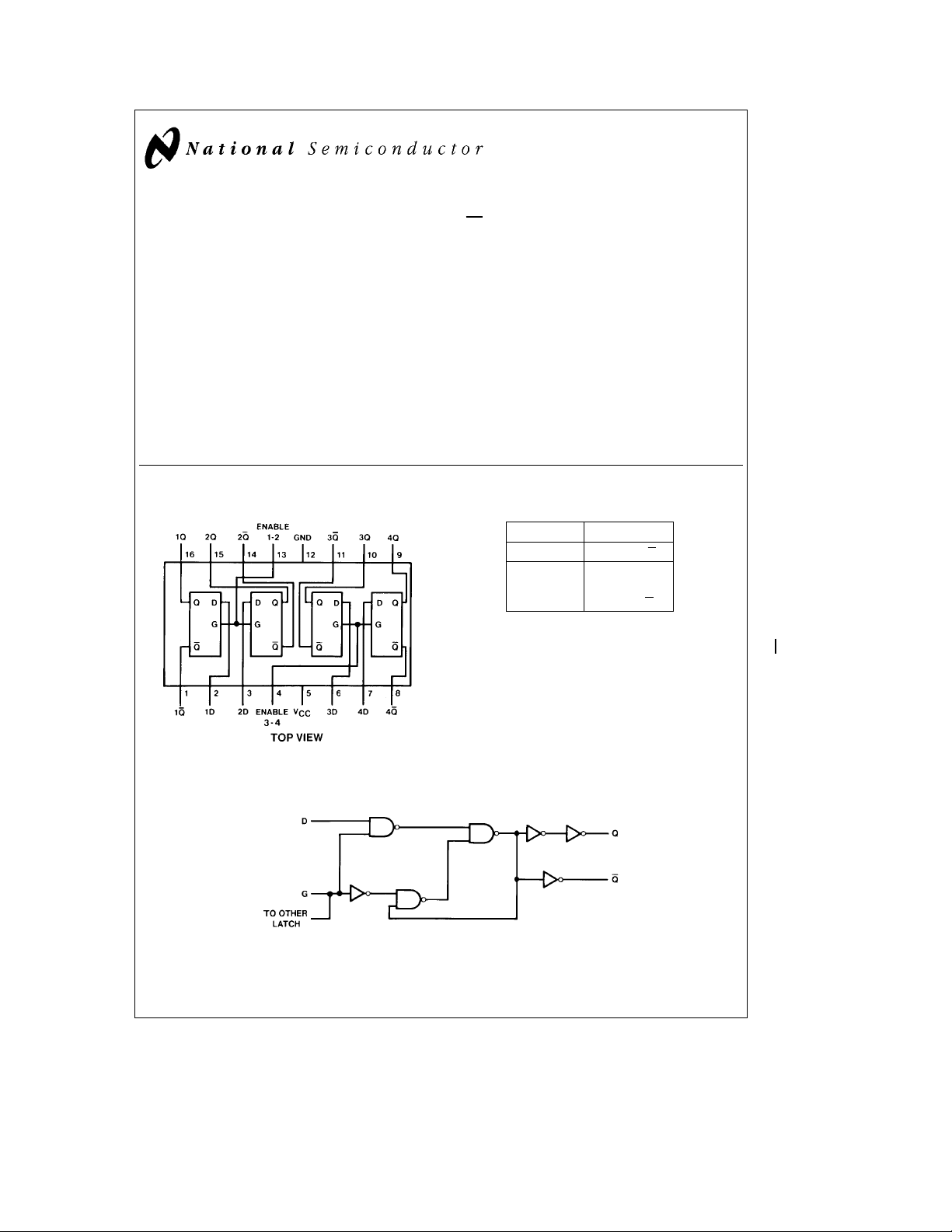
4-Bit Bistable Latch with Q and Q
General Description
This 4-bit latch utilizes advanced silicon-gate CMOS technology to achieve the high noise immunity and low power
consumption normally associated with standard CMOS integrated circuits. These devices can drive 10 LS-TTL loads.
This latch is ideally suited for use as temporary storage for
binary information processing, input/output, and indicator
units. Information present at the data (D) input is transferred
to the Q output when the enable (G) is high. The Q output
will follow the data input as long as the enable remains high.
When the enable goes low, the information that was present
at the data input at the time the transition occurred is retained at the Q output until the enable is permitted to go
high again.
The 54HC/74HC logic family is functionally as well as pinout compatible with the standard 54LS/74LS logic family.
All inputs are protected from damage due to static discharge by internal diode clamps to V
Features
Y
Typical operating frequency: 50 MHz
Y
Typical propagation delay: 12 ns
Y
Wide operating supply voltage range: 2 –6V
Y
Low input current: 1 mA maximum
Y
Low quiescent supply current: 80 m A maximum
(74HC Series)
Y
Fanout of 10 LS-TTL loads
Output
and ground.
CC
MM54HC75/MM74HC75 4-Bit Bistable Latch with Q and Q Output
January 1988
Connection and Logic Diagrams
Dual-In-Line Package
TL/F/5303– 1
Order Number MM54HC75 or MM74HC75
Truth Table
(1 of 4 latches)
Inputs Outputs
DG Q Q
LH L H
HH H L
XLQ
e
H
High Level: LeLow Level
e
X
Don’t Care
e
Q
The level of Q before the transition of G
0
0
TL/F/5303– 2
Q
0
C
1995 National Semiconductor Corporation RRD-B30M105/Printed in U. S. A.
TL/F/5303
Absolute Maximum Ratings (Notes1&2)
Operating Conditions
If Military/Aerospace specified devices are required,
please contact the National Semiconductor Sales
Office/Distributors for availability and specifications.
Supply Voltage (V
CC
)
DC Input Voltage (VIN)
DC Output Voltage (V
OUT
)
Clamp Diode Current (IIK,IOK)
DC Output Current, per pin (I
OUT
)
DC VCCor GND Current, per pin (ICC)
Storage Temperature Range (T
STG
b
b
)
b
0.5 toa7.0V
1.5 to V
CC
0.5 to V
CC
g
g
b
g
65§Ctoa150§C
a
1.5V
a
0.5V
20 mA
25 mA
50 mA
Supply Voltage (V
)26V
CC
DC Input or Output Voltage 0 V
(V
IN,VOUT
)
Operating Temp. Range (TA)
MM74HC
MM54HC
Input Rise or Fall Times
e
V
2.0V(tr,tf) 1000 ns
CC
e
V
4.5V 500 ns
CC
e
V
6.0V 400 ns
CC
Power Dissipation (PD)
(Note 3) 600 mW
S.O. Package only 500 mW
Lead Temp. (T
) (Soldering 10 seconds) 260§C
L
DC Electrical Characteristics (Note 4)
Symbol Parameter Conditions V
CC
A
e
T
25§C
Typ Guaranteed Limits
V
IH
Minimum High Level 2.0V 1.5 1.5 1.5 V
Input Voltage 4.5V 3.15 3.15 3.15 V
6.0V 4.2 4.2 4.2 V
V
IL
Maximum Low Level 2.0V 0.5 0.5 0.5 V
Input Voltage** 4.5V 1.35 1.35 1.35 V
6.0V 1.8 1.8 1.8 V
V
OH
Minimum High Level V
Output Voltage
e
VIHor V
l
IN
I
OUT
IL
s
20 mA 2.0V 2.0 1.9 1.9 1.9 V
l
4.5V 4.5 4.4 4.4 4.4 V
6.0V 6.0 5.9 5.9 5.9 V
e
V
VIHor V
IN
I
l
OUT
I
l
OUT
l
IN
I
OUT
e
V
OL
Maximum Low Level V
Output Voltage
IL
s
4.0 mA 4.5V 4.2 3.98 3.84 3.7 V
l
s
5.2 mA 6.0V 5.7 5.48 5.34 5.2 V
l
VIHor V
IL
s
20 mA 2.0V 0 0.1 0.1 0.1 V
l
4.5V 0 0.1 0.1 0.1 V
6.0V 0 0.1 0.1 0.1 V
e
V
VIHor V
IN
I
l
OUT
I
l
OUT
I
IN
I
CC
Note 1: Absolute Maximum Ratings are those values beyond which damage to the device may occur.
Note 2: Unless otherwise specified all voltages are referenced to ground.
Note 3: Power Dissipation temperature derating Ð plastic ‘‘N’’ package:
Note 4: For a power supply of 5V
with this supply. Worst case V
I
**V
Maximum Input V
Current
Maximum Quiescent V
Supply Current I
g
and VILoccur at V
) occur for CMOS at the higher voltage and so the 6.0V values should be used.
OZ
limits are currently tested at 20% of VCC. The above VILspecification (30% of VCC) will be implemented no later than Q1, CY’89.
IL
IH
e
IN
e
IN
OUT
10% the worst case output voltages (VOH, and VOL) occur for HC at 4.5V. Thus the 4.5V values should be used when designing
IL
s
4.0 mA 4.5V 0.2 0.26 0.33 0.4 V
l
s
5.2 mA 6.0V 0.2 0.26 0.33 0.4 V
l
VCCor GND 6.0V
g
0.1
VCCor GND 6.0V 4.0 40 80 m A
e
0 mA
b
12 mW/§C from 65§Cto85§C; ceramic ‘‘J’’ package:b12 mW/§C from 100§Cto125§C.
e
5.5V and 4.5V respectively. (The VIHvalue at 5.5V is 3.85V.) The worst case leakage current (IIN,ICC, and
CC
74HC 54HC
eb
T
40 to 85§CT
A
g
1.0
Min Max Units
V
§
§
Units
b
b
40
55
eb
A
55 to 125§C
g
CC
a
85
a
125
1.0 mA
C
C
2
 Loading...