

查询MM74HC164MTC供应商
MM74HC164
8-Bit Serial-in/Parallel-out Shift Register
MM74HC164 8-Bit Serial-in/Parallel-out Shift Register
September 1983
Revised January 2005
General Description
The MM74HC164 utilizes advanced silicon-gate CMOS
technology. It has the high noise imm unity and low consumption of standard CMOS integrated circuits. It also
offers speeds comparable to low power Schottky devices.
This 8-bit shift register ha s gat ed serial inputs and CLEAR.
Each register bit is a D-type master/slave flip-flop. Inputs A
& B permit complete control over the incoming data. A
LOW at either or b oth i n puts i nh ibits en try of new data a nd
resets the first flip-flop to the low level at the next clock
pulse. A high level on one input enables the other input
which will then determine the state of the first flip-flop. Data
at the serial inputs may be changed while the clock is HIGH
or LOW, but only information meet ing the setup and hold
time requirements will be entered. Data is serially shifted in
and out of the 8-bit register during the positive going transition of the clock pulse. Clear is independent of the clock
and accomplished by a low level at the CLEAR input.
The 74HC logic family is functionally as well as pin-out
compatible with the standard 74LS logic family. All inputs
are protected from damage due to static discharge by internal diode clamps to V
and ground.
CC
Features
■ Typical operating frequency: 50 MHz
■ Typical propagation delay: 19 ns (clock to Q)
■ Wide operating supply voltage range: 2V to 6V
■ Low input current: 1
■ Low quiescent supply current: 80
(74HC Series)
■ Fanout of 10 LS-TTL loads
µA maximum
µA maximum
Ordering Code:
Order Number
MM74HC164M M14A 14-Lead Small Outline Integrated Circuit (SOIC), JEDEC MS-012, 0.150" Narrow
MM74HC164MX_NL M14A Pb-Free 14-Lead Small Outline Integrated Circuit (SOIC), JEDEC MS-012, 0.150" Narrow
MM74HC164MTC MTC14 14-Lead Thin Shrink Small Outline Package (TSSOP), JEDEC MO-153, 4.4mm Wide
MM74HC164MTCX_NL MTC14 Pb-Free 14-Lead Thin Shrink Small Outline Package (TSSOP), JEDEC MO-153, 4.4mm
MM74HC164N N14A 14-Lead Plastic Dual-In-Line Package (PDIP), JEDEC MS-001, 0.300" Wide
Devices also availab le in Tape and Reel. Specify by appending the suffix letter “X” to the o rdering code.
Pb-Free pac k age per JEDEC J-STD- 020B.
Package
Number
Package Description
Wide
© 2005 Fairchild Semiconductor Corporation DS005315 www.fairchildsemi.com
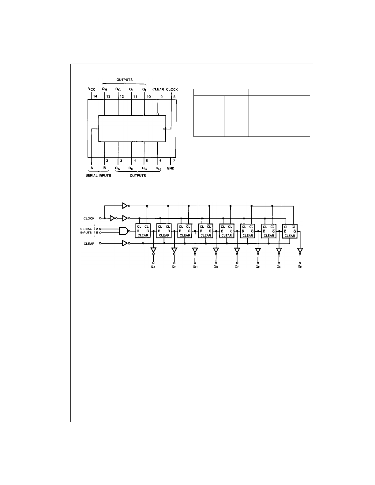
Connection Diagram
MM74HC164
Logic Diagram
Top V iew
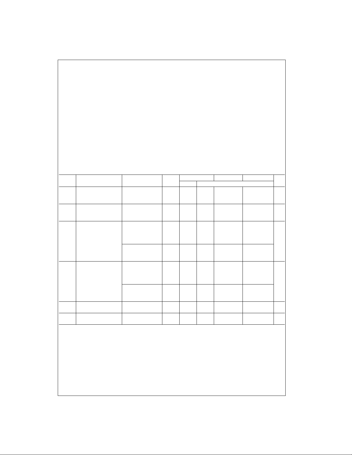
Truth Table
Inputs Outputs
Q
Clear Clock A B Q
A
LXXXLL L
HLXXQ
AOQBO
H ↑ HH HQ
H ↑ LX LQ
H ↑ XL L Q
H = HIGH Level (steady state), L = LOW Level (steady state)
X = Irrelevant (any input, including transitions)
↑ = Transition from LOW-to-HIGH level.
, QBO, QHO = the leve l of QA, QB, or QH, respectively, before the indi-
Q
AO
cated steady state in put conditions were es t ablished.
, QGn = The level of QA or QG before th e most re cent ↑ transition of the
Q
An
clock; indicated a one-bit shift.
... Q
B
Q
An
An
An
Q
Q
Q
H
HO
Gn
Gn
Gn
www.fairchildsemi.com 2
Absolute Maximum Ratings(Note 1)
(Note 2)
Supply Voltage (VCC) −0.5 to +7.0V
DC Input Voltage (V
DC Output Voltage (V
Clamp Diode Current (I
DC Output Current, per pin (I
DC V
or GND Current, per pin (ICC) ±50 mA
CC
Storage Temperature Range (T
Power Dissipation (P
(Note 3) 600 mW
S.O. Package only 500 mW
Lead Temperature (T
(Soldering 10 seconds ) 260
) −1.5 to V
IN
) −0.5 to V
OUT
, IOK) ±20 mA
IK
) ±25 mA
OUT
) −65°C to +150°C
STG
)
D
)
L
CC
CC
Recommended Operating
Conditions
+1.5V
Supply Voltage (V
+0.5V
DC Input or Output Voltage
, V
(V
IN
OUT
Operating Temperature Range (T
Input Rise or Fall Times
, tf) V
(t
r
CC
V
CC
V
Note 1: Absolute Maximum Ratings are those values beyond which damage to the device may occur.
Note 2: Unless otherwise specified all voltages are referenced to ground.
°C
Note 3: Power Dissipation te mperature d erating — pl astic “N” package: −
12 mW/°C from 65°C to 85°C.
CC
)26V
CC
)0V
) −40 +85 °C
A
= 2.0V 1000 ns
= 4.5V 500 ns
= 6.0V 400 ns
Min Max Units
CC
DC Electrical Characteristics (Note 4)
Symbol Parameter Conditions
V
Minimum HIGH Level 2.0V 1.5 1.5 1.5
IH
V
Maximum LOW Level 2.0V 0.5 0.5 0.5
IL
V
Minimum HIGH Level V
OH
Output Voltage |I
V
Maximum LOW Level V
OL
Output Voltage |I
I
Maximum Input V
IN
Current
I
Maximum Quiescent V
CC
Supply Current I
Note 4: For a power supply of 5V ±10% the worst case output voltages (VOH, and VOL) occur for HC at 4.5V. Thus the 4. 5V valu es shou ld be u sed when
designing with this supply. Worst case V
, ICC, and IOZ) occur for CMOS at the higher voltage and so th e 6. 0V values should be used.
rent (I
IN
= VIH or V
IN
OUT
V
IN
|I
OUT
|I
OUT
IN
OUT
V
IN
|I
OUT
|I
OUT
IN
IN
OUT
and VIL occur at V
IH
IL
| ≤ 20 µA 2.0V 2.0 1.9 1.9 1.9
= VIH or V
IL
| ≤ 4.0 mA 4.5V 4.2 3.98 3.84 3.7
| ≤ 5.2 mA 6.0V 5.7 5.48 5.34 5.2
= VIH or V
IL
| ≤ 20 µA 2.0V 0 0.1 0.1 0.1
= VIH or V
IL
| ≤ 4.0 mA 4.5V 0.2 0.26 0.33 0.4
| ≤ 5.2 mA 6.0V 0.2 0.26 0.33 0.4
= VCC or GND 6.0V ±0.1 ±1.0 ±1.0 µA
= VCC or GND 6.0V 8.0 80 160 µA
= 0 µA
CC
V
CC
6.0V 4.2 4.2 4.2
6.0V 1.8 1.8 1.8
4.5V 4.5 4.4 4.4 4.4
6.0V 6.0 5.9 5.9 5.9
4.5V 0 0.1 0.1 0.1
6.0V 0 0.1 0.1 0.1
= 5.5V and 4.5V respectively. (The VIH value at 5.5V is 3.85V.) The worst case leakage cur-
TA = 25°CTA = −40 to 85°CTA = −55 to 125°C
Typ Guaranteed Limits
MM74HC164
V
Units
VInput Voltage 4.5V 3.15 3.15 3.15
VInput Voltage 4.5V 1.35 1.35 1.35
V
V
3 www.fairchildsemi.com
 Loading...