National Semiconductor MM54HC161, MM54HC163, MM74HC161, MM74HC163 Service Manual

MM74HC160 Synchronous
Decade Counter with Asynchronous Clear
MM54HC161/MM74HC161 Synchronous
Binary Counter with Asynchronous Clear
MM54HC162/MM74HC162 Synchronous
Decade Counter with Synchronous Clear
MM54HC163/MM74HC163 Synchronous
Binary Counter with Synchronous Clear
General Description
The MM54HC160/MM74HC160, MM54HC161/
MM74HC161, MM54HC162/MM74HC162, and
MM54HC163/MM74HC163 synchronous presettable counters utilize advanced silicon-gate CMOS technology and internal look-ahead carry logic for use in high speed counting
applications. They offer the high noise immunity and low
power consumption inherent to CMOS with speeds similar
to low power Schottky TTL. The ’HC160 and the ’HC162 are
4 bit decade counters, and the ’HC161 and the ’HC163 are
4 bit binary counters. All flip-flops are clocked simultaneously on the low to high transition (positive edge) of the CLOCK
input waveform.
These counters may be preset using the LOAD input. Presetting of all four flip-flops is synchronous to the rising edge
of CLOCK. When LOAD is held low counting is disabled and
the data on the A, B, C, and D inputs is loaded into the
counter on the rising edge of CLOCK. If the load input is
taken high before the positive edge of CLOCK the count
operation will be unaffected.
All of these counters may be cleared by utilizing the CLEAR
input. The clear function on the MM54HC162/MM74HC162
and MM54HC163/MM74HC163 counters are synchronous
to the clock. That is, the counters are cleared on the positive edge of CLOCK while the clear input is held low.
The MM54HC160/MM74HC160 and MM54HC161/
MM74HC161 counters are cleared asynchronously. When
the CLEAR is taken low the counter is cleared immediately
regardless of the CLOCK.
Two active high enable inputs (ENP and ENT) and a RIPPLE CARRY (RC) output are provided to enable easy cascading of counters. Both ENABLE inputs must be high to
count. The ENT input also enables the RC output. When
enabled, the RC outputs a positive pulse when the counter
overflows. This pulse is approximately equal in duration to
the high level portion of the Q
to successive cascaded stages to facilitate easy implementation of N-bit counters.
All inputs are protected from damage due to static discharge by diodes to V
CC
Features
Y
Typical operating frequency: 40 MHz
Y
Typical propagation delay; clock to Q: 18 ns
Y
Low quiescent current: 80 mA maximum (74HC Series)
Y
Low input current: 1 mA maximum
Y
Wide power supply range: 2–6V
output. The RC output is fed
A
and ground.
74HC160/MM54/74HC161/MM54/74HC162/MM54/74HC163
January 1992
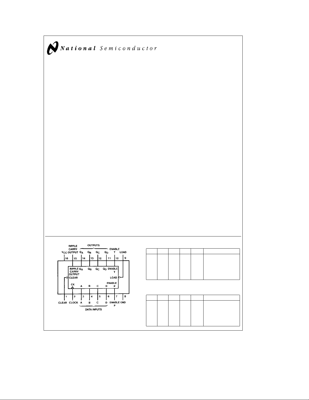
Connection Diagram
Order Number MM54HC161/162/163
or MM74HC160/161/162/163
C
1995 National Semiconductor Corporation RRD-B30M115/Printed in U. S. A.
TL/F/5008
TL/F/5008– 1
Truth Tables
’HC160/HC161
CLK CLR ENP ENT Load Function
X L X X X Clear
X H H L H Count & RC disabled
X H L H H Count disabled
X H L L H Count & RC disabled
H X X L Load
u
H H H H Increment Counter
u
Hehigh level, Lelow level
e
don’t care,
X
CLK CLR ENP ENT Load Function
u
X H H L H Count & RC disabled
X H L H H Count disabled
X H L L H Count & RC disabled
u
u
e
low to high transition
u
’HC162/HC163
L X X X Clear
H X X L Load
H H H H Increment Counter

Absolute Maximum Ratings (Notes1&2)
Operating Conditions
If Military/Aerospace specified devices are required,
please contact the National Semiconductor Sales
Office/Distributors for availability and specifications.
Supply Voltage (V
CC
)
DC Input Voltage (VIN)
DC Output Voltage (V
OUT
)
Clamp Diode Current (IIK,IOK)
DC Output Current, per pin (I
OUT
)
DC VCCor GND Current, per pin (ICC)
Storage Temperature Range (T
STG
b
b
)
b
0.5 toa7.0V
1.5 to V
CC
0.5 to V
CC
g
g
b
g
65§Ctoa150§C
a
1.5V
a
0.5V
20 mA
25 mA
50 mA
Power Dissipation (PD)
Supply Voltage (V
DC Input or Output Voltage 0 V
(V
IN,VOUT
Operating Temp. Range (T
MM74HC
MM54HC
Input Rise or Fall Times
)26V
CC
)
e
V
2.0V(tr,tf) 1000 ns
CC
e
4.5V 500 ns
V
CC
e
6.0V 400 ns
V
CC
(Note 3) 600 mW
S.O. Package only 500 mW
Lead Temp. (T
) (Soldering 10 seconds) 260§C
L
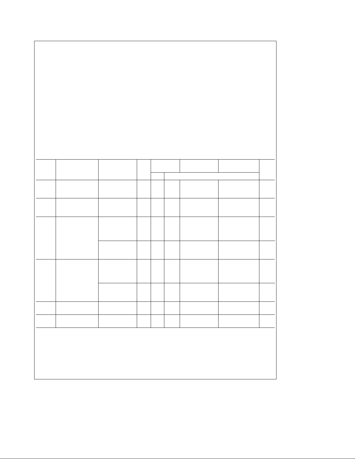
DC Electrical Characteristics (Note 4)
Symbol Parameter Conditions V
CC
A
e
T
25§C
Typ Guaranteed Limits
V
IH
Minimum High Level 2.0V 1.5 1.5 1.5 V
Input Voltage 4.5V 3.15 3.15 3.15 V
6.0V 4.2 4.2 4.2 V
V
IL
Maximum Low Level 2.0V 0.5 0.5 0.5 V
Input Voltage** 4.5V 1.35 1.35 1.35 V
6.0V 1.8 1.8 1.8 V
V
OH
Minimum High Level V
Output Voltage
e
VIHor V
l
I
IN
OUT
IL
s
20 mA 2.0V 2.0 1.9 1.9 1.9 V
l
4.5V 4.5 4.4 4.4 4.4 V
6.0V 6.0 5.9 5.9 5.9 V
e
V
VIHor V
IN
I
l
OUT
I
l
OUT
l
I
IN
OUT
e
V
OL
Maximum Low Level V
Output Voltage
IL
s
4.0 mA 4.5V 4.2 3.98 3.84 3.7 V
l
s
5.2 mA 6.0V 5.7 5.48 5.34 5.2 V
l
VIHor V
IL
s
20 mA 2.0V 0 0.1 0.1 0.1 V
l
4.5V 0 0.1 0.1 0.1 V
6.0V 0 0.1 0.1 0.1 V
e
V
VIHor V
IN
I
l
OUT
I
l
OUT
I
IN
I
CC
Note 1: Absolute Maximum Ratings are those values beyond which damage to the device may occur.
Note 2: Unless otherwise specified all voltages are referenced to ground.
Note 3: Power Dissipation temperature derating Ð plastic ‘‘N’’ package:
Note 4: For a power supply of 5V
with this supply. Worst case V
I
**V
Maximum Input V
Current
Maximum Quiescent V
Supply Current I
g
and VILoccur at V
) occur for CMOS at the higher voltage and so the 6.0V values should be used.
OZ
limits are currently tested at 20% of VCC. The above VILspecification (30% of VCC) will be implemented no later than Q1, CY’89.
IL
IH
e
IN
e
IN
OUT
10% the worst case output voltages (VOH, and VOL) occur for HC at 4.5V. Thus the 4.5V values should be used when designing
IL
s
4.0 mA 4.5V 0.2 0.26 0.33 0.4 V
l
s
5.2 mA 6.0V 0.2 0.26 0.33 0.4 V
l
VCCor GND 6.0V
g
0.1
VCCor GND 6.0V 8.0 80 160 mA
e
0 mA
b
12 mW/§C from 65§Cto85§C; ceramic ‘‘J’’ package:b12 mW/§C from 100§Cto125§C.
e
5.5V and 4.5V respectively. (The VIHvalue at 5.5V is 3.85V.) The worst case leakage current (IIN,ICC, and
CC
74HC 54HC
eb
T
40 to 85§CT
A
g
1.0
Min Max Units
)
A
b
b
40
55
eb
A
55 to 125§C
g
a
a
1.0 mA
CC
85
125
V
C
§
C
§
Units
2
 Loading...