

查询MM54C90供应商
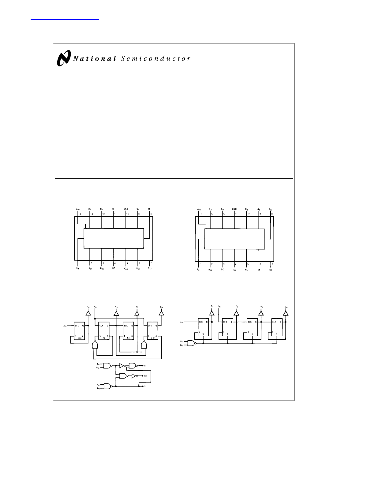
MM54C90/MM74C90 4-Bit Decade Counter
MM54C93/MM74C93 4-Bit Binary Counter
General Description
The MM54C90/MM74C90 decade counter and the
MM54C93/MM74C93 binary counter and complementary
MOS (CMOS) integrated circuits constructed with N- and
P-channel enhancement mode transistors. The 4-bit decade
counter can reset to zero or preset to nine by applying appropriate logic level on the R
Also, a separate flip-flop on the A-bit enables the user to
operate it as a divide-by-2, 5 or 10 frequency counter. The
4-bit binary counter can be reset to zero by applying high
logic level on inputs R
the A-bit enables the user to operate it as a divide-by-2, -8,
or -16 divider. Counting occurs on the negative going edge
of the input pulse.
Connection and Logic Diagrams
MM54C90/MM74C90
Dual-In-Line Package
01,R02,R91
and R02, and a separate flip-flop on
01
and R92inputs.
February 1988
All inputs are protected against static discharge damage.
Features
Y
Wide supply voltage range 3V to 15V
Y
Guaranteed noise margin 1V
Y
High noise immunity 0.45 VCC(typ.)
Y
Low power Fan out of 2
TTL compatiblity driving 74L
Y
The MM54C93/MM74C93 follows the MM54L93/
MM74L93 Pinout
MM54C93/MM74C93
Dual-In-Line Package
MM54C90/MM74C90 4-Bit Decade Counter
MM54C93/MM74C93 4-Bit Binary Counter
Top View
M54C90/MM74C90
C
1995 National Semiconductor Corporation RRD-B30M105/Printed in U. S. A.
TL/F/5889
TL/F/5889– 2
Top View
Order Number MM54C90 or MM74C93
MM54C93/MM74C93
TL/F/5889– 1
TL/F/5889– 4
TL/F/5889– 3
Absolute Maximum Ratings
If Military/Aerospace specified devices are required,
please contact the National Semiconductor Sales
Office/Distributors for availability and specifications.
Voltage at Any Pin (Note 1)
Operating Temperature Range (TA)
MM54C90, MM54C93
MM74C90, MM74C93
b
0.3V to V
b
b
a
0.3V
CC
55§Ctoa125§C
40§Ctoa85§C
Power Dissipation (P
Dual-In-Line 700 mW
Small Outline 500 mW
Operating V
CC
Absolute Maximum V
Storage Temperature Range (T
Lead Temperature (TL)
(Soldering, 10 seconds) 260
)
D
Range 3V to 15V
CC
S
b
)
65§Ctoa150§C
DC Electrical Characteristics Min/Max limits apply across temperature range unless otherwise noted
Symbol Parameter Conditions Min Typ Max Units
CMOS TO CMOS
V
IN(1)
V
IN(0)
V
OUT(1)
V
OUT(0)
I
IN(1)
I
IN(0)
I
CC
Logical ‘‘1’’ Input Voltage V
Logical ‘‘0’’ Input Voltage V
Logical ‘‘1’’ Output Voltage V
Logical ‘‘0’’ Output Voltage V
Logical ‘‘1’’ Input Current V
Logical ‘‘0’’ Input Current V
Supply Current V
CMOS/LPTTL INTERFACE
V
IN(1)
V
IN(0)
V
OUT(1)
V
OUT(0)
Logical ‘‘1’’ Input Voltage
MM54C90, MM54C93 V
MM74C90, MM74C93 V
Logical ‘‘0’’ Input Voltage
MM54C90, MM54C93 V
MM74C90, MM74C93 V
Logical ‘‘1’’ Output Voltage
MM54C90, MM54C93 V
MM74C90, MM74C93 V
Logical ‘‘0’’ Output Voltage
MM54C90, MM54C93 V
MM74C90, MM74C93 V
OUTPUT DRIVE (See 54C/74C Family Characteristics Data Sheet) (Short Circuit Current)
I
SOURCE
I
SOURCE
I
SINK
I
SINK
Note 1: ‘‘Absolute Maximum Ratings’’ are those values beyond which the safety of the device cannot be guaranteed. Except for ‘‘Operating Temperature Range’’,
they are not meant to imply that the devices should be operated at these limits. The table of ‘‘Electrical Characteristics’’ provides conditions for actual device
operation.
Output Source Current V
(P-Channel) T
Output Source Current V
(P-Channel) T
Output Sink Current V
(N-Channel) T
Output Sink Current V
(N-Channel) T
e
5V 3.5 V
CC
e
10V 8.0 V
V
CC
e
5V 1.5 V
CC
e
10V 2.0 V
V
CC
e
eb
5V, I
CC
e
10V, I
V
CC
e
5V, I
CC
e
V
10V, I
CC
e
15V, V
CC
e
15V, V
CC
e
15V 0.05 300 mA
CC
e
4.5V V
CC
e
4.75V V
CC
e
4.5V 0.8 V
CC
e
4.75V 0.8 V
CC
e
4.5V, I
CC
e
4.75V, I
CC
e
4.5V, I
CC
e
4.75V, I
CC
e
5V, V
CC
e
25§C
A
e
10V, V
CC
e
25§C
A
e
5V, V
CC
e
25§C
A
e
10V, V
CC
e
25§C
A
10 mA 4.5 V
O
eb
10 mA 9.0 V
O
ea
10 mA 0.5 V
O
ea
10 mA 1.0 V
O
e
15V 0.005 1.0 mA
IN
e
0V
IN
eb
360 mA 2.4 V
O
eb
360 mA 2.4 V
O
eb
360 mA 0.4 V
O
eb
360 mA 0.4 V
O
e
0V
OUT
e
0V
OUT
e
V
OUT
CC
e
V
OUT
CC
CC
CC
b
b
b
1.0
b
b
1.75
8.0
b
0.005 mA
1.5 V
1.5 V
b
3.3 mA
b
15 mA
1.75 3.6 mA
8.0 16 mA
18V
C
§
AC Electrical Characteristics* T
e
A
25§C, C
e
50 pF, unless otherwise specified
L
Symbol Parameter Conditions Min Typ Max Units
t
pd0,tpd1
t
pd0,tpd1
t
pd0,tpd1
Propagation Delay Time V
to Q
from A
IN
Propagation Delay Time from V
A
IN
Propagation Delay Time from V
A
IN
A
to QB(MM54C93/MM74C93) V
to QB(MM54C90/MM74C90) V
e
5V 200 400 ns
CC
e
V
10 80 150 ns
CC
e
5V 450 850 ns
CC
e
10V 160 300 ns
CC
e
5V 450 800 ns
CC
e
10V 160 300 ns
CC
2

AC Electrical Characteristics* T
e
A
25§C, C
e
50 pF, unless otherwise specified (Continued)
L
Symbol Parameter Conditions Min Typ Max Units
t
pd0,tpd1
t
pd0,tpd1
t
pd0,tpd1
t
pd0,tpd1
t
pd0,tpd1
t
pd0,tpd1
t
pd0,tpd1
t
PW
t
PW
t
PW
tr,t
f
t
W
f
MAX
C
IN
C
PD
*AC Parameters are guaranteed by DC correlated testing.
Note 1: ‘‘Absolute Maximum Ratings’’ are those values beyond which the safety of the device cannot be guaranteed. Except for ‘‘Operating Temperature Range’’,
they are not meant to imply that the devices should be operated at these limits. The table of ‘‘Electrical Characteristics’’ provides conditions for actual device
operation.
Note 2: Capacitance is guaranteed by periodic testing.
Note 3: C
AN-90.
Propagation Delay Time V
to QC(MM54C93/MM74C93) V
from A
IN
Propagation Delay Time from V
to QC(MM54C93/MM74C93) V
A
IN
Propagation Delay Time from V
to QD(MM54C93/MM74C93) V
A
IN
Propagation Delay Time from V
to QD(MM54C90/MM74C90) V
A
IN
Propagation Delay Time from V
or R02to QA,QB,QCor Q
R
01
(MM54C93/MM74C93)
Propagation Delay Time from V
or R02to QA,QB,QCor Q
R
01
(MM54C90/MM74C90)
Propagation Delay Time from V
or R92to QAor Q
R
91
(MM54C90/MM74C90)
Min. R01or R02Pulse Width V
(MM54C93/MM74C93) V
Min. R01or R02Pulse Width V
(MM54C90/MM74C90) V
Min. R91or R92Pulse Width V
(MM54C90/MM74C90) V
Maximum Clock Rise V
and Fall Time V
D
D
D
Minimum Clock Pulse Width V
Maximum Clock Frequency V
Input Capacitance Any Input (Note 2) 5 pF
Power Dissipation Capacitance Per Package (Note 3) 45 pF
determines the no load ac power consumption of any CMOS device. For complete explanation see 54C/74C Family Characteristics application noteÐ
PD
e
5V 500 1050 ns
CC
e
10 200 400 ns
CC
e
5V 500 1000 ns
CC
e
10V 200 400 ns
CC
e
5V 600 1200 ns
CC
e
10V 250 500 ns
CC
e
5V 450 800 ns
CC
e
10V 160 300 ns
CC
e
5V 150 300 ns
CC
e
V
10V 75 150 ns
CC
e
5V 200 400 ns
CC
e
V
10V 75 150 ns
CC
e
5V 250 500 ns
CC
e
V
10V 100 200 ns
CC
e
5V 600 250 ns
CC
e
10V 30 125 ns
CC
e
5V 600 250 ns
CC
e
10V 300 125 ns
CC
e
5V 500 200 ns
CC
e
10V 250 100 ns
CC
e
10V 15 ms
CC
e
10V 5 ms
CC
e
5V 250 100 ns
CC
e
10V 100 50 ns
V
CC
e
5V 2 MHz
CC
e
10V 5 MHz
V
CC
AC Test Circuits
MM54C90/MM74C90
Clock rise and fall time t
MM54C93/MM74C93
e
e
t
r
f
TL/F/5889– 5
20 ns
Clock rise and fall time t
e
e
t
r
f
TL/F/5889– 6
20 ns
3

Switching Time Waveforms
Truth Table
MM54C90/MM74C90 4-Bit Decade Counter
BCD Count Sequence
Count
0LLLL
1LLLH
2LLHL
3LLHH
4LHLL
5LHLH
6LHHL
7LHHH
8HLLL
9HLLH
Output QAis connected to Input B for
BCD count.
e
H
High Level
e
Low Level
L
e
Irrelevant
X
Reset/Count Function Table
Reset Inputs Output
R01R02R91R92QDQCQBQ
HHL XLLLL
HHX LLLLL
XXHHHLLH
X L X L Count
L X L X Count
L X X L Count
X L L X Count
Output
QDQCQBQ
Note 1: MM54C90, MM74C90 and MM54C93,
MM74C93 are solid line waveforms. Dashed line
waveforms are for MM54C90/MM74C90 only.
TL/F/5889– 7
MM54C93/MM74C93 4-Bit Binary Counter
Binary Count Sequence
A
Count
Output
QDQCQBQ
A
0LLLL
1LLLH
2LLHL
3LLHH
4LHLL
5LHLH
6LHHL
7LHHH
8HLLL
9HLLH
10 H L H L
11 H L H H
12 H H L L
13 H H L H
14 H H H L
15 H H H H
Output QAis connected to input B for
binary count sequence.
e
H
A
L
X
High Level
e
Low Level
e
Irrelevant
Reset/Count Function Table
Reset
Inputs
R
01R02QDQCQBQA
Output
HHLLLL
L X Count
X L Count
4

Physical Dimensions inches (millimeters)
Order Number MM54C90J, MM54C93J, MM74C90J or MM74C93J
Ceramic Dual-In-Line Package (J)
NS Package Number J14A
5

Physical Dimensions inches (millimeters) (Continued)
Order Number MM54C90N, MM54C93N, MM74C90N or MM74C93N
Molded Dual-In-Line Package (N)
NS Package Number N14A
MM54C93/MM74C93 4-Bit Binary Counter
MM54C90/MM74C90 4-Bit Decade Counter
LIFE SUPPORT POLICY
NATIONAL’S PRODUCTS ARE NOT AUTHORIZED FOR USE AS CRITICAL COMPONENTS IN LIFE SUPPORT
DEVICES OR SYSTEMS WITHOUT THE EXPRESS WRITTEN APPROVAL OF THE PRESIDENT OF NATIONAL
SEMICONDUCTOR CORPORATION. As used herein:
1. Life support devices or systems are devices or 2. A critical component is any component of a life
systems which, (a) are intended for surgical implant support device or system whose failure to perform can
into the body, or (b) support or sustain life, and whose be reasonably expected to cause the failure of the life
failure to perform, when properly used in accordance support device or system, or to affect its safety or
with instructions for use provided in the labeling, can effectiveness.
be reasonably expected to result in a significant injury
to the user.
National Semiconductor National Semiconductor National Semiconductor National Semiconductor
Corporation Europe Hong Kong Ltd. Japan Ltd.
1111 West Bardin Road Fax: (
Arlington, TX 76017 Email: cnjwge@tevm2.nsc.com Ocean Centre, 5 Canton Rd. Fax: 81-043-299-2408
Tel: 1(800) 272-9959 Deutsch Tel: (
Fax: 1(800) 737-7018 English Tel: (
National does not assume any responsibility for use of any circuitry described, no circuit patent licenses are implied and National reserves the right at any time without notice to change said circuitry and specifications.
Fran3ais Tel: (
Italiano Tel: (
a
49) 0-180-530 85 86 13th Floor, Straight Block, Tel: 81-043-299-2309
a
49) 0-180-530 85 85 Tsimshatsui, Kowloon
a
49) 0-180-532 78 32 Hong Kong
a
49) 0-180-532 93 58 Tel: (852) 2737-1600
a
49) 0-180-534 16 80 Fax: (852) 2736-9960
 Loading...