

February 2000
LM4120
Precision Micropower Low Dropout Voltage Reference
LM4120 Precision Micropower Low Dropout Voltage Reference
General Description
The LM4120 is a precision low power low dropout bandgap
voltage reference with up to 5 mA output current source and
sink capability.
This series reference operates with input voltages as low as
2V and up to 12V consuming 160 µA(Typ.) supply current. In
power down mode, device current drops to less than 2 µA.
The LM4120 comes in two grades (A and Standard) and
seven voltage options for greater flexibility. The best grade
devices (A) have an initial accuracy of 0.2%, while the standard have an initial accuracy of 0.5%, both with a tempco of
50ppm/˚C guaranteed from −40˚C to +125˚C.
The very low dropout voltage, low supply current and
power-down capability of the LM4120 makes this product an
ideal choice for battery powered and portable applications.
The device performance is guaranteed over the industrial
temperature range (−40˚C to +85˚C), while certain specs are
guaranteed over the extended temperature range (−40˚C to
+125˚C). Please contact National for full specifications over
the extended temperature range. The LM4120 is available in
a standard 5-pin SOT-23 package.
Features
n Small SOT23-5 package
n Low dropout voltage: 120 mV Typ
n High output voltage accuracy: 0.2
n Source and Sink current output:
n Supply current: 160 µA Typ.
n Low Temperature Coefficient: 50 ppm/˚C
n Enable pin
n Fixed output voltages: 1.8, 2.048, 2.5, 3.0, 3.3, 4.096
and 5.0V
n Industrial temperature Range: −40˚C to +85˚C
n (For extended temperature range, −40˚C to 125˚C,
contact National Semiconductor)
@
±
1mA
5mA
Applications
n Portable, battery powered equipment
n Instrumentation and process control
n Automotive & Industrial
n Test equipment
n Data acquisition systems
n Precision regulators
n Battery chargers
n Base stations
n Communications
n Medical equipment
%
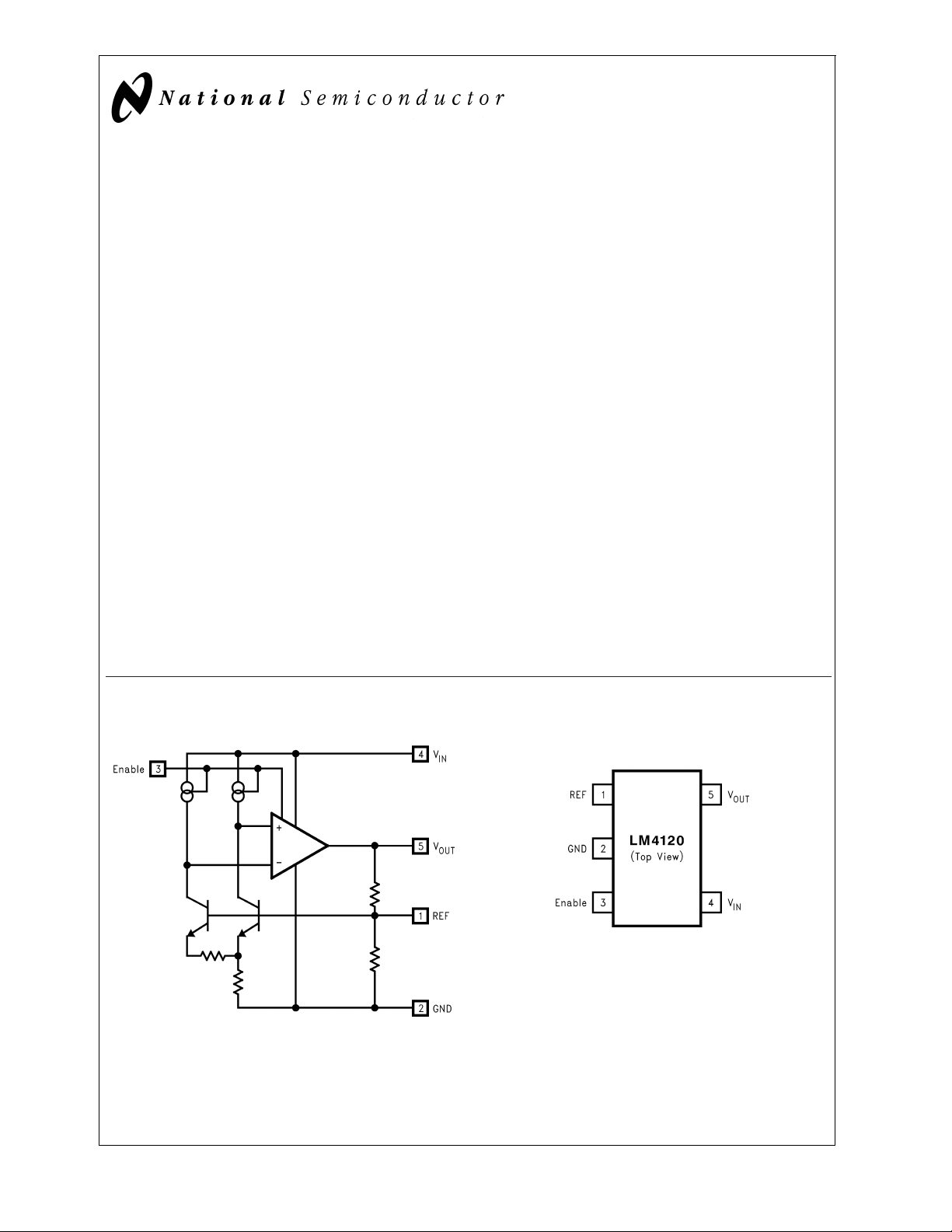
Functional Block Diagram
DS101047-1
Connection Diagram
DS101047-2
Refer to the Ordering Information Table in this Data Sheet for Specific
Part Number
SOT23-5 Surface Mount Package
© 2000 National Semiconductor Corporation DS101047 www.national.com
Ordering Information
LM4120
Industrial Temperature Range (−40˚C to + 85˚C)
Initial Output Voltage Accuracy at 25˚C
And Temperature Coefficient
0.2%, 50 ppm/˚C max (A grade)
0.5%, 50 ppm/˚C max
LM4120 Supplied as
1000 Units, Tape and
Reel
LM4120AIM5-1.8 LM4120AIM5X-1.8 R21A
LM4120AIM5-2.0 LM4120AIM5X-2.0 R14A
LM4120AIM5-2.5 LM4120AIM5X-2.5 R08A
LM4120AIM5-3.0 LM4120AIM5X-3.0 R15A
LM4120AIM5-3.3 LM4120AIM5X-3.3 R16A
LM4120AIM5-4.1 LM4120AIM5X-4.1 R17A
LM4120AIM5-5.0 LM4120AIM5X-5.0 R18A
LM4120IM5-1.8 LM4120IM5X-1.8 R21B
LM4120IM5-2.0 LM4120IM5X-2.0 R14B
LM4120IM5-2.5 LM4120IM5X-2.5 R08B
LM4120IM5-3.0 LM4120IM5X-3.0 R15B
LM4120IM5-3.3 LM4120IM5X-3.3 R16B
LM4120IM5-4.1 LM4120IM5X-4.1 R17B
LM4120IM5-5.0 LM4120IM5X-5.0 R18B
SOT-23 Package Marking Information
Only four fields of marking are possible on the SOT-23’s small surface. This
table gives the meaning of the four fields.
Field Information
First Field:
R=Reference
Second and third Field:
21=1.800V Voltage Option
14=2.048V Voltage Option
08=2.500V Voltage Option
15=3.000V Voltage Option
16=3.300V Voltage Option
17=4.096V Voltage Option
18=5.000V Voltage Option
Fourth Field:
A-B=Initial Reference Voltage Tolerance
=
±
A
B
%
0.2
=
±
%
0.5
LM4120 Supplied as
3000 Units, Tape and
Reel
Top
Marking
www.national.com 2
LM4120
Absolute Maximum Ratings (Note 1)
If Military/Aerospace specified devices are required,
please contact the National Semiconductor Sales Office/
Distributors for availability and specifications.
Lead Temperature:
Soldering, (10 sec.) +260˚C
Vapor Phase (60 sec.) +215˚C
Infrared (15 sec.) +220˚C
Maximum Voltage on input or
enable pins −0.3V to 14V
Output Short-Circuit Duration Indefinite
Power Dissipation (T
MA05B package − θ
= 25˚C) (Note 2):
A
JA
280˚C/W
Operating Range (Note 1)
Storage Temperature Range −65˚C to +150˚C
Ambient Temperature Range −40˚C to +85˚C
Junction Temperature Range −40˚C to +125˚C
Power Dissipation 350 mW
ESD Susceptibility (Note 3)
Human Body Model
Machine Model
2kV
200V
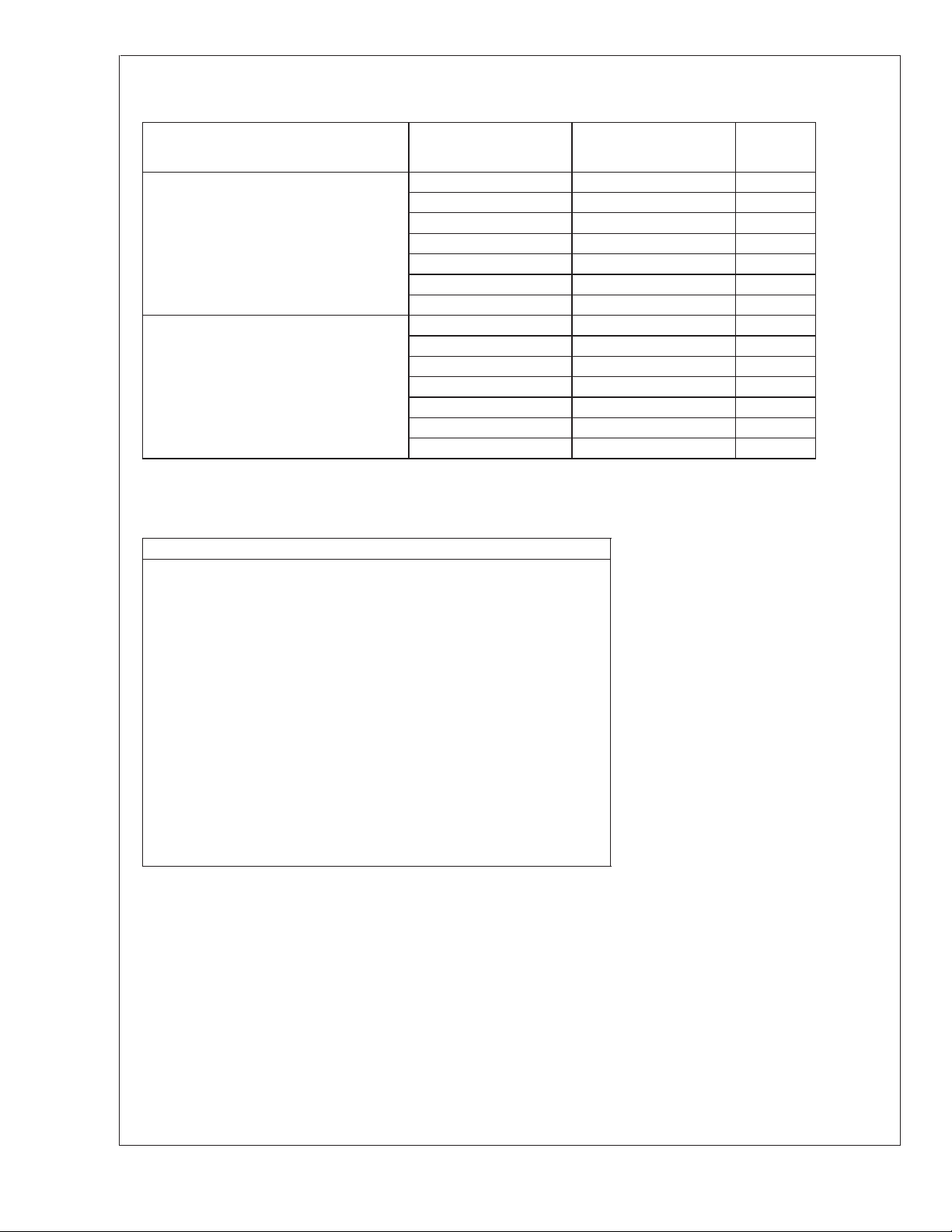
Electrical Characteristics
LM4120-1.8V, 2.048V and 2.5V
=
25˚C. Limits with standard typeface are for T
j
Unless otherwise specified V
=
25˚C, and limits in boldface type apply over the −40˚C ≤ T
=
3.3V, I
IN
perature range.
Symbol Parameter Conditions Min (Note 5) Typ (Note 4) Max (Note 5) Units
Output Voltage Initial
Accuracy
LM4120A-1.800
V
OUT
LM4120A-2.048
LM4120A-2.500
LM4120-1.800
LM4120-2.048
LM4120-2.500
TCV
∆V
∆V
V
V
/˚C Temperature Coefficient −40˚C ≤ TA≤ +125˚C 14 50 ppm/˚c
OUT
/∆V
OUT
/∆I
OUT
IN−VOUT
N
Line Regulation 3.3V ≤ VIN≤ 12V 0.0007 0.008
IN
≤ 1 mA 0.03 0.08
LOAD
≤ 5 mA 0.01 0.04
LOAD
≤ 0 mA 0.04 0.12
LOAD
≤ −1 mA 0.01
LOAD
Load Regulation
LOAD
Dropout Voltage (Note 6)
0mA≤I
1mA≤I
−1 mA ≤ I
−5 mA ≤ I
=0mA 45 65
I
LOAD
= +1 mA 120 150
I
LOAD
I
= +5 mA 180 210
LOAD
Output Noise Voltage (Note 8) 0.1 Hz to 10 Hz 20 µV
10 Hz to 10 kHz 36 µV
I
S
I
SS
Supply Current 160 250
Power-down Supply Current Enable=0.4V
−40˚C ≤ T
≤ +85˚C
J
Enable=0.2V
V
H
Logic High Input Voltage 2.4 V
2.4
V
L
I
H
Logic Low Input Voltage 0.4 V
Logic High Input Current 7 15 µA
LOAD
=
0, C
OUT
=
0.01µF, T
≤ +85˚C tem-
A
±
0.2
±
0.5
0.01
0.17
0.1
80
180
250
275
1
2 µA
0.2
=
T
A
j
%
%
%
/V
%
/mA
mV
PP
PP
µA
www.national.com3
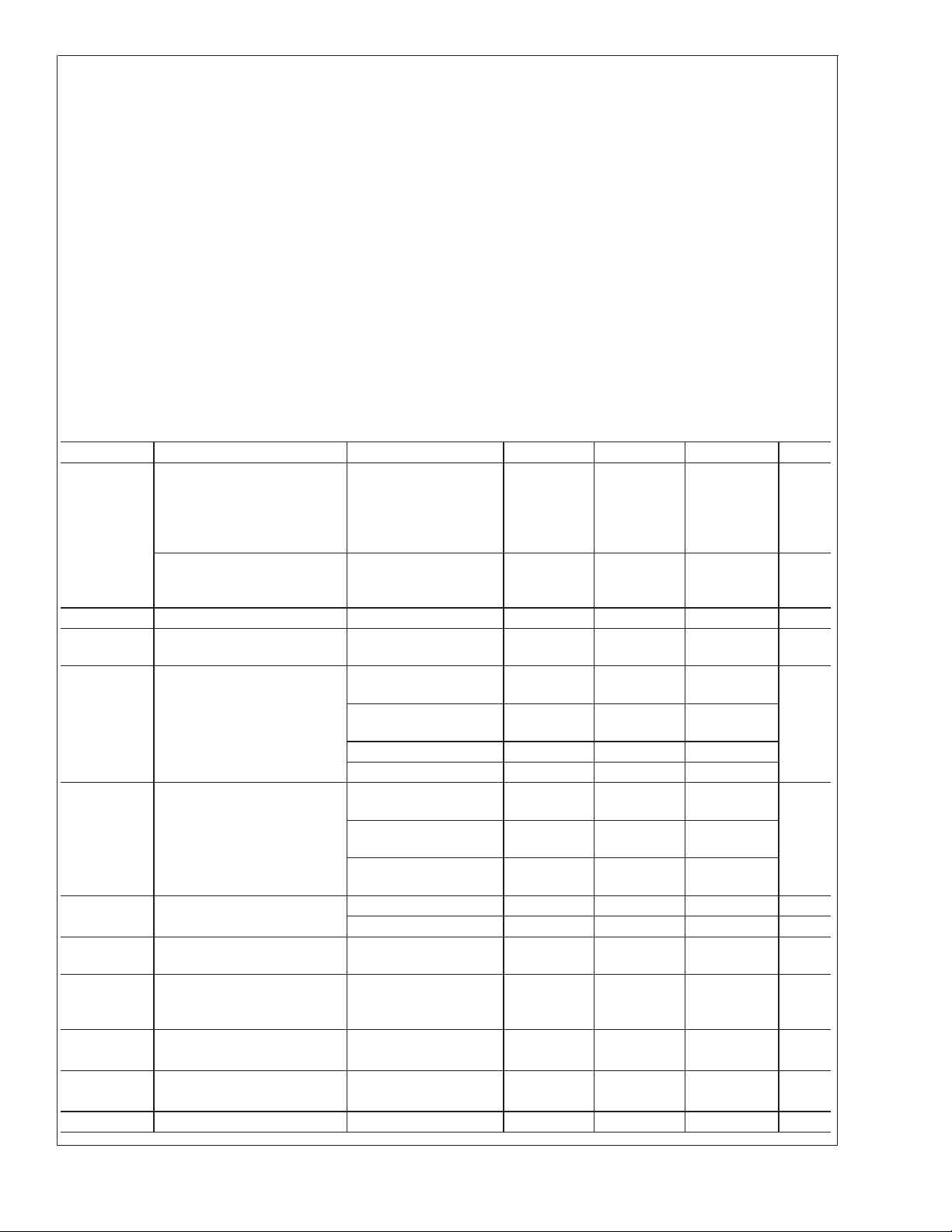
Electrical Characteristics
LM4120-1.8V, 2.048V and 2.5V
LM4120
=
25˚C. Limits with standard typeface are for T
Unless otherwise specified V
=
25˚C, and limits in boldface type apply over the −40˚C ≤ T
j
=
3.3V, I
IN
temperature range. (Continued)
Symbol Parameter Conditions Min (Note 5) Typ (Note 4) Max (Note 5) Units
I
L
I
SC
Logic Low Input Current 0.1 µA
Short Circuit Current
=
3.3V, V
V
IN
=
V
12V, V
IN
=
015
OUT
630
=
017
OUT
630
Hyst Thermal Hysteresis
−40˚C ≤ T
≤ 125˚C 0.5 mV/V
A
(Note 7)
∆V
OUT
Long Term Stability
1000 hrs.@25˚C 100 ppm
(Note 9)
LOAD
=
0, C
OUT
=
0.01µF, T
≤ +85˚C
A
Electrical Characteristics
LM4120-3.0V, 3.3V, 4.096V and 5.0V
=
0.01µF, T
T
≤ +85˚C temperature range.
A
=
T
A
25˚C. Limits with standard typeface are for T
j
Unless otherwise specified V
=
25˚C, and limits in boldface type apply over the −40˚C ≤
j
Symbol Parameter Conditions Min (Note 5) Typ (Note 4) Max (Note 5) Units
Output Voltage Initial
Accuracy
LM4120A-3.000
LM4120A-3.300
V
OUT
LM4120A-4.096
LM4120A-5.000
LM4120-3.000
LM4120-3.300
LM4120-4.096
LM4120-5.000
TCV
∆V
∆V
V
V
/˚C Temperature Coefficient −40˚C ≤ TA≤ +125˚C 14 50 ppm/˚c
OUT
/∆V
OUT
/∆I
OUT
IN−VOUT
N
Line Regulation (V
IN
Load Regulation
LOAD
Dropout Voltage (Note 6)
+ 1V) ≤ VIN≤ 12V 0.0007 0.008
OUT
0mA≤I
1mA≤I
−1 mA ≤ I
−5 mA ≤ I
=0mA 45 65
I
LOAD
= +1 mA 120 150
I
LOAD
I
= +5 mA 180 210
LOAD
≤ 1 mA 0.03 0.08
LOAD
≤ 5 mA 0.01 0.04
LOAD
≤ 0 mA 0.04 0.12
LOAD
≤ −1 mA 0.01
LOAD
Output Noise Voltage (Note 8) 0.1 Hz to 10 Hz 20 µV
10 Hz to 10 kHz 36 µV
I
S
I
SS
Supply Current 160 250
Power-down Supply Current Enable=0.4V
−40˚C ≤ T
≤ +85˚C
J
Enable=0.2V
=
IN
+ 1V, I
V
OUT
LOAD
±
0.2
±
0.5
0.01
0.17
0.1
80
180
250
275
1
2 µA
=
T
A
j
mA
=
0, C
OUT
=
%
%
%
/V
%
/mA
mV
PP
PP
µA
www.national.com 4

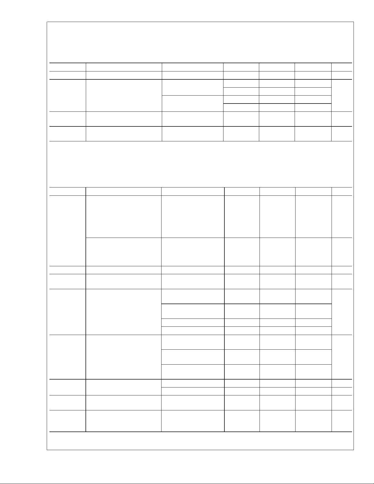
Electrical Characteristics
LM4120-3.0V, 3.3V, 4.096V and 5.0V
=
0.01µF, T
T
≤ +85˚C temperature range. (Continued)
A
=
T
A
25˚C. Limits with standard typeface are for T
j
Unless otherwise specified V
=
25˚C, and limits in boldface type apply over the −40˚C ≤
j
=
IN
+ 1V, I
V
OUT
Symbol Parameter Conditions Min (Note 5) Typ (Note 4) Max (Note 5) Units
V
H
Logic High Input Voltage 2.4 V
2.4
V
L
I
H
I
L
I
SC
Logic Low Input Voltage 0.4 V
Logic High Input Current 7 15 µA
Logic Low Input Current 0.1 µA
=
015
OUT
630
=
12V, V
IN
=
017
OUT
Short Circuit Current
V
V
630
Hyst Thermal Hysteresis
−40˚C ≤ T
≤ 125˚C 0.5 mV/V
A
(Note 7)
∆V
OUT
Long Term Stability
1000 hrs.@25˚C 100 ppm
(Note 9)
Note 1: “Absolute Maximum Ratings” indicate limits beyond which damage to the device may occur. Operating Ratings indicate conditions for which the device is
intended tobe functional, but do not guarantee specific performance limits. For guaranteed specifications and test conditions, see Electrical Characteristics. The guaranteed specifications apply only for the test conditions listed. Some performance characteristics may degrade when the device is not operated under the listed test
conditions.
Note 2: Without PCB copper enhancements. The maximum power dissipation must be de-rated at elevated temperatures andis limited by T
temperature), θ
−TA)/θ
J-A
Note 3: The human body model is a 100 pF capacitor discharged through a 1.5 kΩ resistor into each pin. The machine model is a 200 pF capacitor discharged di-
rectly into each pin.
Note 4: Typical numbers are at 25˚C and represent the most likely parametric norm.
Note 5: Limits are 100%production tested at 25˚C. Limits over the operating temperature range are guaranteed through correlation using Statistical Quality Control
(SQC) methods. The limits are used to calculate National’s Averaging Outgoing Quality Level (AOQL).
Note 6: Dropout voltage is the differential voltage between V
1V for others.For 1.8V option, dropout voltage is not guaranteed over temperature. A parasitic diode exists between input and output pins; it will conduct if V
pulled to a higher voltage than V
Note 7: Thermal hysteresis is defined as the change in +25˚C output voltage before and after exposing the device to temperature extremes.
Note 8: Output noise voltage is proportional to V
Note 9: Long term stability is change in V
(junction to ambient thermal resistance) and TA(ambient temperature). The maximum power dissipation at any temperature is: PDiss
J-A
up to the value listed in the Absolute Maximum Ratings.
and VINat which V
OUT
.
IN
for other voltage option is calculated using (V
OUT.VN
at 25˚C measured continuously during 1000 hrs.
REF
changes ≤ 1%from V
OUT
N(1.8V)
OUT
/1.8)*V
=
at V
3.3V for 1.8V, 2.0V, 2.5V and V
IN
(2.5V)=(36µVPP/1.8)*2.5=46µVPP.
OUT.VN
=
LOAD
0.2
(maximum junction
JMAX
0, C
MAX
OUT
=
(T
OUT
OUT
LM4120
=
mA
JMAX
+
is
LM4120 Typical Operating Characteristics Unless otherwise specified, V
=
I
LOAD
0, C
Long Term Drift
OUT
=
0.022µF, T
=
A
DS101047-12
25˚C and V
=
.
V
EN
IN
Typical Temperature Drift
Short Circuit Current vs
Temperature
DS101047-13
IN
=
3.3V, V
OUT
www.national.com5
=
2.5V,
DS101047-14

LM4120 Typical Operating Characteristics Unless otherwise specified, V
I
LOAD
LM4120
=
0, C
OUT
=
0.022µF, T
=
25˚C and V
A
=
. (Continued)
V
EN
IN
IN
=
3.3V, V
OUT
=
2.5V,
Dropout Voltage vs Output Error
DS101047-15
Load Regulation
Dropout Voltage vs Load Current
DS101047-33
GND Pin Current
Line Regulation
DS101047-17
GND Pin Current at No Load
vs Temperature
GND Pin Current vs Load
DS101047-18
DS101047-22
0.1Hz to 10Hz output Noise
DS101047-19
DS101047-23
DS101047-21
Output Impedance vs Frequency
DS101047-24
www.national.com 6

LM4120
LM4120 Typical Operating Characteristics Unless otherwise specified, V
=
I
0, C
LOAD
PSRR vs Frequency
Load Step Response
OUT
=
0.022µF, T
=
25˚C and V
A
DS101047-25
=
. (Continued)
V
EN
IN
Start-Up Response
Load Step Response
Enable Response
DS101047-26
Line Step Response
IN
=
3.3V, V
OUT
=
2.5V,
DS101047-27
Thermal Hysteresis
DS101047-28
DS101047-31
Enable Pin Current
DS101047-29
DS101047-16
DS101047-30
www.national.com7

Pin Functions
Output (Pin 5): Reference Output.
LM4120
Input (Pin 4):Positive Supply.
Ground (Pin 2):Negative Supply or Ground Connection.
Enable (Pin 3):Pulled to input for normal operation. Forcing
this pin to ground will turn-off the output.
REF (Pin 1):REF Pin. This pin should be left unconnected.
Application Hints
The standard application circuit for the LM4120 is shown in
Figure 1
pacitors in the range of 0.022µF to 0.047µF. Note that
0.022µF is the minimum requiredoutput capacitor. These capacitors typically have an ESR of about 0.1 to 0.5Ω. Smaller
ESR can be tolerated, however larger ESR can not. The output capacitor can be increased to improve load transient response, up to about 1µF. However, values above 0.047µF
must be tantalum. With tantalum capacitors, in the 1µF
range, a small capacitor between the output and the reference pin is required. This capacitor will typically be in the
50pF range. Care must be taken when using output capacitors of 1µF or larger. These application must be thoroughly
tested over temperature, line and load.
An input capacitor is typically not required. However, a 0.1µF
ceramic can be used to help prevent line transients from entering the LM4120. Larger input capacitors should be tantalum or aluminium.
The reference pin is sensitive to noise, and capacitive loading. Therefore, the PCB layout should isolate this pin as
much as possible.
The enable pin is an analog input with very little hysteresis.
About 6µA into this pin is required to turn the part on, and it
must be taken close to GND to turn the part off (see spec.
table for thresholds). There is a
pin of about 0.003V/µS to prevent glitches on the output. All
of these conditions can easily be met with ordinary CMOS or
TTL logic. If the shutdown feature is not required, then this
pin can safely be connected directly to the input supply.
Floating this pin is not recommended.
. It is designed to be stable with ceramic output ca-
minimum
slew rate on this
DS101047-32
FIGURE 1.
Input Capacitor
Noise on the power-supply input can effect the output noise,
but can be reduced by using an optional bypass capacitor
between the input pin and the ground.
Printed Circuit Board Layout Consideration
The mechanical stress due to PC board mounting can cause
the output voltage to shift from its initial value. References in
SOT packages are generally less prone to assembly stress
than devices in Small Outline (SOIC) package.
To reduce the stress-related output voltage shifts, mount the
reference on the low flex areas of the PC board such as near
to the edge or the corner of the PC board.
www.national.com 8

LM4120
Typical Application Circuits
Voltage Reference with Negative Output
DS101047-3
Precision High Current Low Dropout Regulator
Voltage Reference with Complimentary Output
DS101047-6
Precision High Current Low Droput Regulator
Precision High Current
Negative Voltage Regulator
DS101047-7
Stacking Voltage References
DS101047-4
DS101047-8
DS101047-5
www.national.com9
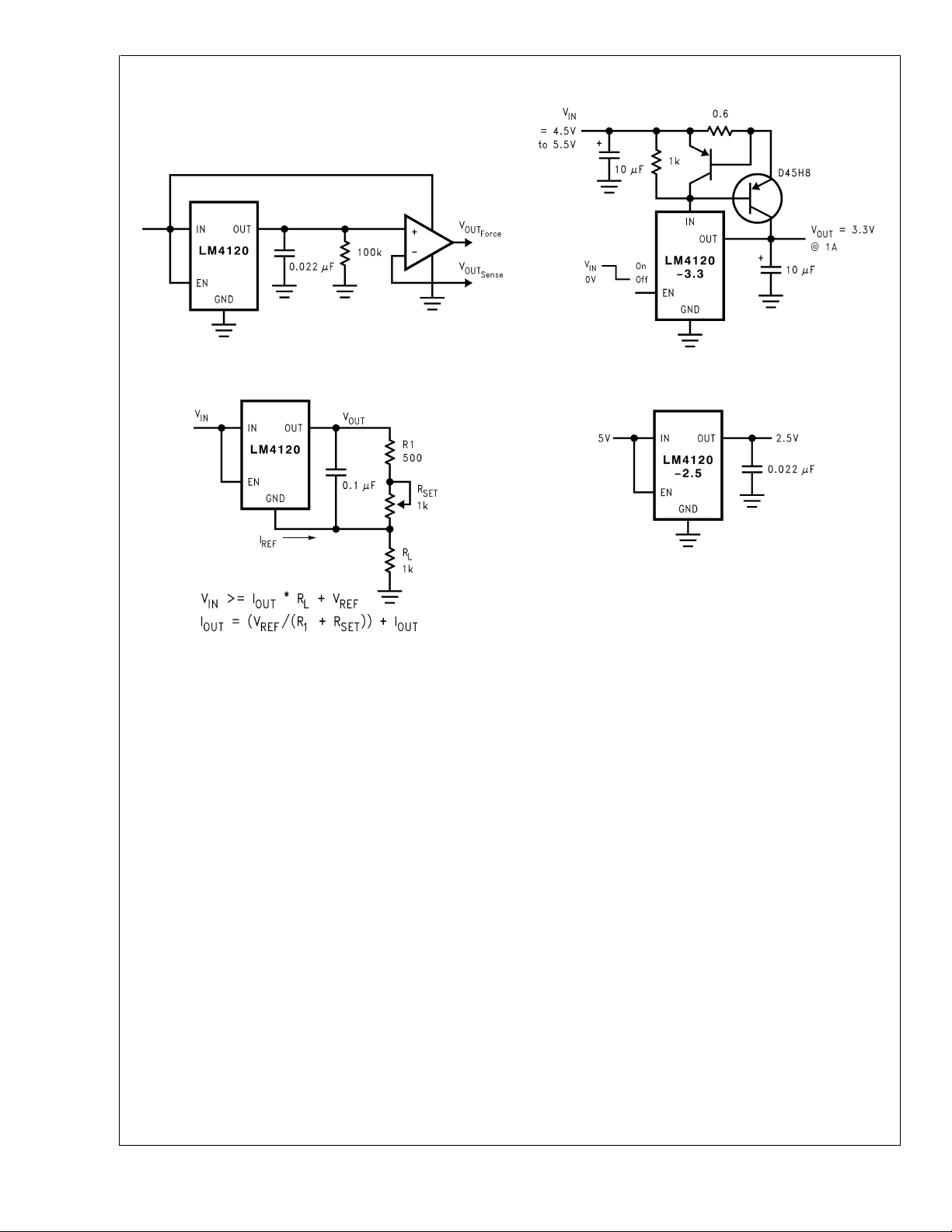
Typical Application Circuits
(Continued)
LM4120
Precision Voltage Reference
with Force and Sense Output
Precision Regulator with Current Limiting Circuit
Programmable Current Source
DS101047-10
DS101047-9
DS101047-11
Power Supply Splitter
DS101047-20
www.national.com 10
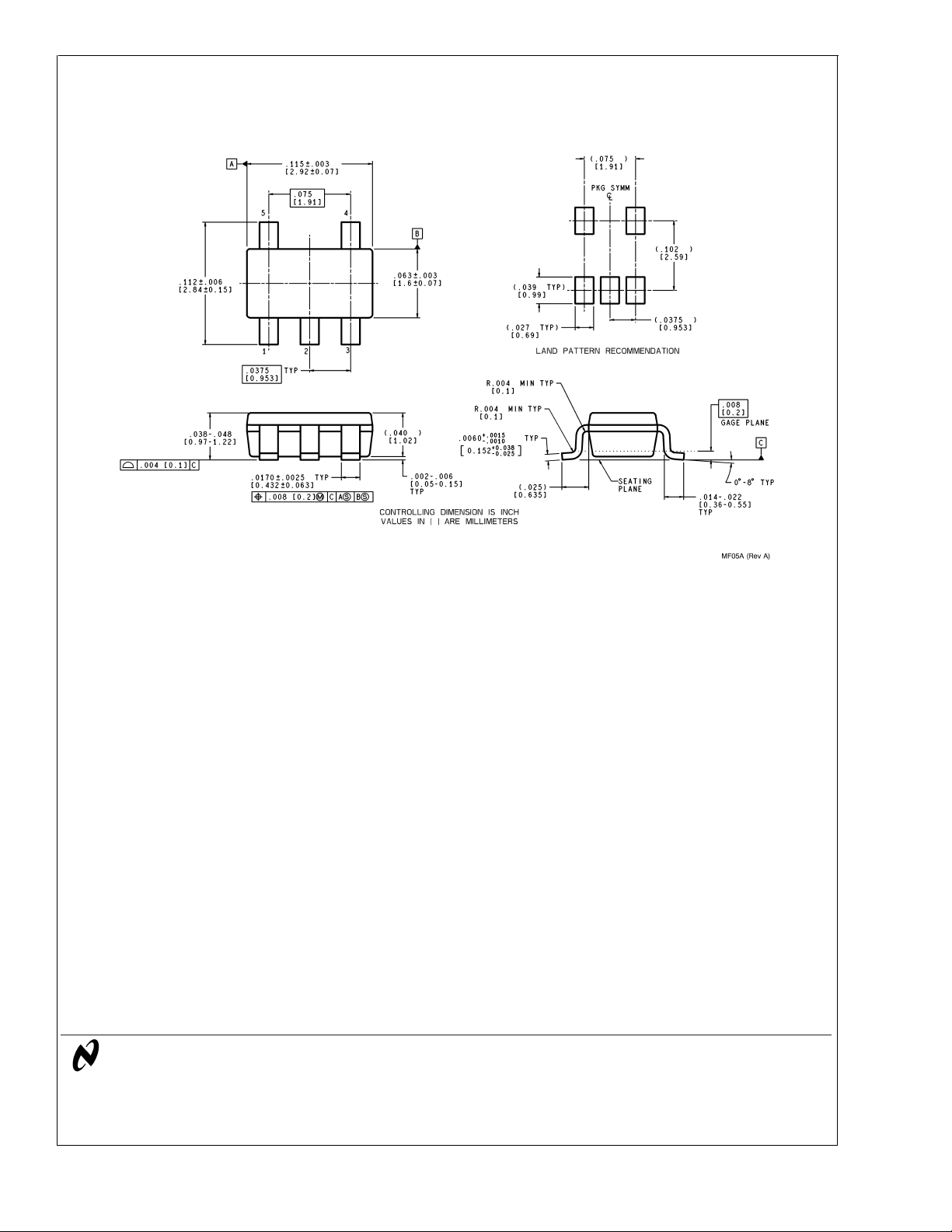
Physical Dimensions inches (millimeters) unless otherwise noted
LM4120 Precision Micropower Low Dropout Voltage Reference
LIFE SUPPORT POLICY
NATIONAL’S PRODUCTS ARE NOT AUTHORIZED FOR USE AS CRITICAL COMPONENTS IN LIFE SUPPORT
DEVICES OR SYSTEMS WITHOUT THE EXPRESS WRITTEN APPROVAL OF THE PRESIDENT AND GENERAL
COUNSEL OF NATIONAL SEMICONDUCTOR CORPORATION. As used herein:
1. Life support devices or systems are devices or
systems which, (a) are intended for surgical implant
into the body, or (b) support or sustain life, and
whose failure to perform when properly used in
accordance with instructions for use provided in the
2. A critical component is any component of a life
support device or system whose failure to perform
can be reasonably expected to cause the failure of
the life support device or system, or to affect its
safety or effectiveness.
labeling, can be reasonably expected to result in a
significant injury to the user.
National Semiconductor
Corporation
Americas
Tel: 1-800-272-9959
Fax: 1-800-737-7018
Email: support@nsc.com
www.national.com
National does not assume any responsibility for use of any circuitry described, no circuit patent licenses are implied and National reserves the right at any time without notice to change said circuitry and specifications.
National Semiconductor
Europe
Fax: +49 (0) 180-530 85 86
Email: europe.support@nsc.com
Deutsch Tel: +49 (0) 69 9508 6208
English Tel: +44 (0) 870 24 0 2171
Français Tel: +33 (0) 1 41 91 8790
National Semiconductor
Asia Pacific Customer
Response Group
Tel: 65-2544466
Fax: 65-2504466
Email: ap.support@nsc.com
National Semiconductor
Japan Ltd.
Tel: 81-3-5639-7560
Fax: 81-3-5639-7507

WWW.ALLDATASHEET.COM
Copyright © Each Manufacturing Company.
All Datasheets cannot be modified without permission.
This datasheet has been download from :
www.AllDataSheet.com
100% Free DataSheet Search Site.
Free Download.
No Register.
Fast Search System.
www.AllDataSheet.com
 Loading...