


October 20, 2008
LP8900
Ultra Low Noise, Dual 200mA Linear Regulator for RF/
Analog Circuits
LP8900 Ultra Low Noise, Dual 200mA Linear Regulator for RF/Analog Circuits
General Description
The LP8900 is a dual linear regulator capable of supplying
200mA output current per regulator. Designed to meet the
requirements of RF/Analog circuits, the LP8900 provides low
device noise, High PSRR, low quiescent current and superior
line transient response figures.
Using new innovative design techniques the LP8900 offers
class-leading device noise performance without a noise bypass capacitor.
The LP8900 is designed to be stable with space saving
ceramic capacitors as small as 0402 case size, enabling a
solution size <4mm 2.
Performance is specified for a -40°C to 125°C junction
temperature range.
Output voltage options are available between 1.2V and 3.6V,
for availability please contact your local NSC sales office.
Typical Application Circuit
Features
Operation from 1.8V to 5.5V Input
■
1% accuracy Over Temperature
■
Output Voltage from 1.2V to 3.6V
■
6µV
■
■
■
■
■
■
■
Output Voltage Noise
RMS
PSRR 75dB at 1kHz
110mV Dropout at 200mA load
48µA Quiescent Current per regulator
80µs Start-Up time
Stable with Ceramic Capacitors as small as 0402
Thermal-Overload and Short-Circuit Protection
Package
6 pin micro SMD (1.5mm x 1.1mm)
Applications
Battery Operated Devices
■
Hand-Held Information Appliances
■
Noise Sensitive RF Applications
■
DC/DC Convertor Post Regulation/Filter
■
30039302
© 2008 National Semiconductor Corporation 300393 www.national.com

Pin Descriptions
LP8900
Pin No. Symbol Name and Function
A1 V
B1 GND Common Ground.
C1 V
C2 V
B2 V
A2 V
Connection Diagram
Packages
EN
1
Enable Input; Enables the Regulator when ≥ 1.2V.
Disables the Regulator when ≤ 0.4V.
Enable Input has an internal 3MΩ pull-down resistor to GND.
EN
2
Enable Input; Enables the Regulator when ≥ 1.2V.
Disables the Regulator when ≤ 0.4V.
Enable Input has an internal 3MΩ pull-down resistor to GND.
2 Voltage output. A Low ESR Ceramic Capacitor should be
OUT
connected from this pin to GND. (See Application Information)
Connect this output to the load circuit.
IN
Voltage Supply Input. A 1.0µF capacitor should be connected from
this pin to GND.
1 Voltage output. A Low ESR Ceramic Capacitor should be
OUT
connected from this pin to GND. (See Application Information)
Connect this output to the load circuit.
6 Bump Thin Micro SMD, Large Bump
See NS package number TLA06
www.national.com 2
30039306

Ordering Information (6-Bump Micro SMD)
Only available as Lead Free.
Output Voltage (V) Grade
Vout 1 Vout2
2.8V 2.8V LP8900TLE_3333 LP8900TLX_3333
2.8V 2.7V LP8900TLE_AAEB LP8900TLX_AAEB
*2.8V 1.2V LP8900TLE_AAEC LP8900TLX_AAEC
* Contact your local NSC Sales Office for availability
Order Number Supplied as 250 Units,
Tape and Reel
Order Number Supplied as 3000 Units,
Tape and Reel
LP8900
3 www.national.com
Absolute Maximum Ratings
LP8900
(Notes 1, 2)
If Military/Aerospace specified devices are required,
please contact the National Semiconductor Sales Office/
Distributors for availability and specifications.
VIN, V
VEN : Voltage to GND -0.3 to (VIN + 0.3V) to 6.5V
Junction Temperature 150°C
Pins: Voltage to GND
OUT
-0.3 to 6.5V
(max)
Operating Ratings (Note 1)
Input Voltage Range 1.8 to 5.5V
Recommended Load Current per
channel 200mA
Junction Temperature -40°C to 125°C
Ambient Temperature TA Range
(Note 6)
-40°C to 85°C
Lead/Pad Temp. (Note 3)
Micro SMD 260°C
Storage Temperature -65 to 150°C
Continuous Power Dissipation
Internally Limited
(Note 4)
ESD (Note 5)
Human Body Model 2KV
Machine Model 200V
Thermal Properties (Note 1)
Junction To Ambient Thermal
Resistance(Note 7)
θJA JEDEC Board
(Note 8)
θJA 4 Layer Board
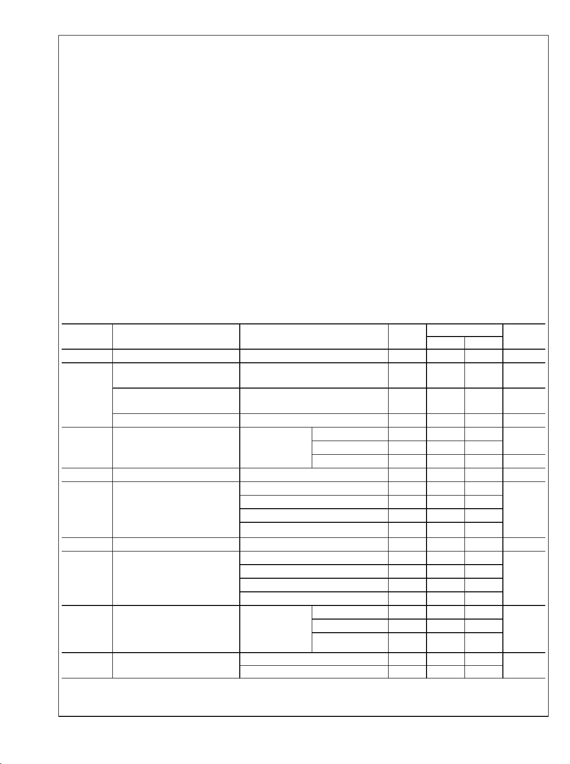
Electrical Characteristics
Unless otherwise noted, VEN =1.2V, VIN = V
V
OUT2. CIN
= C
OUT
= 1µF, I
= 1.0mA .
OUT
Typical values and limits appearing in normal type apply for TA = 25°C. Limits appearing in boldface type apply over the full junction
temperature range for operation, −40 to +125°C. (Note 9)
Symbol Parameter Conditions Typ
V
ΔV
IN
OUT
Input Voltage (Note 10)
Output Voltage Tolerance VIN = V
Line Regulation Error VIN = V
Load Regulation Error I
V
DO
I
LOAD
I
Q
I
SC
Dropout Voltage(Note 11)
Load Current (Note 12)
Quiescent Current V
Short Circuit Current Limit VIN = 3.6V (Note 13) 600 900
PSRR Power Supply Rejection Ratio
(Note 14)
e
n
T
SHUTDOWN
Output noise Voltage (Note 14)
Thermal Shutdown Temperature 155
+ 0.5V, or 1.8V, whichever is higher , where V
OUT
is the higher of V
OUT
Min Max
1.8 5.5 V
OUT(NOM)
I
= 1mA
LOAD
OUT(NOM)
I
= 1mA
OUT
= 1mA to 200mA , V
OUT
I
= 200mA
OUT
+ 0.5V to 5.5V
+0.5V to 5.5V,
OUT
V
= 3.6V
OUT
V
= 2.8V 110
OUT
V
= 1.8V 185
OUT
= 2.8V 4 9
-1.0 1.0 %
0.05 %/V
55
0
= 1.2V, V
EN1
V
= 1.2V, V
EN1
V
= 1.2V, V
EN1
VEN ≤ 0.4V
f = 1kHz, I
f = 10kHz, I
f = 100kHz, I
f = 1MHz, I
BW = 10Hz to
100kHz,
VIN = 4.2V, C
1.0µF
= 0V I
EN2
= 1.2V I
EN2
= 1.2V I
EN2
= 200mA 75
OUT
= 200mA 65
OUT
= 200mA 45
OUT
= 200mA 30
OUT
=
OUT
I
OUT
I
OUT
I
OUT
= 0mA
OUT
= 0mA
OUT
= 200mA
OUT
= 0mA
= 1mA
= 200mA
48
85
210
0.003
6
10
6
Hysteresis 15
Limit
82
164
260
200
120
200
1.0
OUT1
108°C/W
172°C/W
and
Units
mV
mV
mA
µA
mA
dB
µV
RMS
°C
www.national.com 4

Electrical Characteristics con't.
Unless otherwise noted, VEN =1.2V, VIN = V
V
OUT2. CIN
= C
OUT
= 1µF, I
OUT
= 1mA.
Typical values and limits appearing in normal type apply for TA = 25°C. Limits appearing in boldface type apply over the full junction
temperature range for operation, −40 to +125°C. (Note 9)
Symbol Parameter Conditions Typ
Enable Control Characteristics
I
EN
Maximum Input Current at
VEN Input(Note 15)
V
IL
V
IH
Low Input Threshold VIN = 1.8V to 5.5V
High Input Threshold VIN = 1.8V to 5.5V
Timing\Transient Characteristics(Note 14)
T
ON
T
OFF
Transient
Turn On Time To 95% Level
Turn Off Time 5% of V
Line Transient Response |δV
Load Transient Response |δV
Response
Overshoot on Start-up 0 1 %
+ 0.5V, or 1.8V, whichever is higher, where V
OUT
VEN = 0V, VIN = 5.5V
is the higher of V
OUT
0.003
VEN = VIN = 5.5V 4
80
0.4 1 ms
1
80
70
OUT
OUT
|
|
V
OUT(nom)
OUT(NOM),IOUT
T
= T
rise
= 30µs
fall
δVIN = 600mV
T
= T
rise
= 1µs I
fall
= 0mA
= 1 mA to 200mA
OUT
I
= 200mA to 1mA
OUT
Limit
Min Max
0.4 V
1.2
200 µs
OUT1
and
(pk - pk)
LP8900
Units
µA
V
mV
mV
Note 1: Absolute Maximum Ratings are limits beyond which damage can occur. Operating Ratings are conditions under which operation of the device is
guaranteed. Operating Ratings do not imply guaranteed performance limits. For guaranteed performance limits and associated test conditions, see the Electrical
Characteristics tables.
Note 2: All Voltages are with respect to the potential at the GND pin.
Note 3: For further information on these packages please refer to the following application notes,AN-1112 Micro SMD Wafer Level Chip Scale Package.
Note 4: Internal thermal shutdown circuitry protects the device from permanent damage.
Note 5: The human body model is 100pF discharged through a 1.5kΩ resistor into each pin. The machine model is a 200pF capacitor discharged directly into
each pin.
Note 6: The maximum ambient temperature (T
dissipation of the device in the application (P
following equation: T
Note 7: Junction to ambient thermal resistance is dependant on the application and board layout. In applications where high maximum power dissipation is
possible, special care must be paid to thermal dissipation issues in board design.
Note 8: Full details can be found in JESD61-7
Note 9: All limits are guaranteed. All electrical characteristics having room-temperature limits are tested during production at TJ = 25°C or correlated using
Statistical Quality Control methods. Operation over the temperature specification is guaranteed by correlating the electrical characteristics to process and
temperature variations and applying statistical process control.
Note 10: The minimum input voltage = V
Note 11: Dropout voltage is voltage difference between input and output at which the output voltage drops to 100mV below its nominal value. This parameter is
only specified for output voltages above 1.8V.
Note 12: The device maintains the regulated output voltage without a load.
Note 13: Short circuit current is measured with V
Note 14: This electrical specification is guaranteed by design.
Note 15: Enable Pin has an internal 3MΩ typical, resistor connected to GND.
Note 16: The capacitor tolerance should be 30% or better over temperature. The full operating conditions for the application should be considered when selecting
a suitable capacitor to ensure that the minimum value of capacitance is always met. Recommended capacitor type is X7R or X5R. (See capacitor section in
Applications Hints)
A(max)
= T
J(max-op)
- (θJA × P
OUT(NOM)
) is dependant on the maximum operating junction temperature (T
A(max)
), and the junction to ambient thermal resistance of the part / package in the application (θJA), as given by the
D(max)
).
D(max)
+ 0.5V or 1.8V, whichever is greater.
pulled to 0V.
OUT
= 125°C), the maximum power
J(max-op)
Recommended Capacitor Specifications
Symbol Parameter Conditions Typ
C
IN
C
OUT
Input Capacitor
Output Capacitor
Capacitance
(Note 16)
ESR
5 www.national.com
Limit
Min Max
Units
1.0 0.33 10 µF
1.0 0.33 4.7
5 500
mΩ

Typical Performance Characteristics. Unless otherwise specified, C
V
OUT(NOM)
LP8900
+ 1.0V or 1.8V whichever is greater, TA = 25°C, V
OUT(NOM)
= 2.85V , Enable pin is tied to VIN.
IN
= C
=1.0µF Ceramic, VIN =
OUT
Power Supply Rejection Ratio
Noise Density
30039310
Power Supply Rejection Ratio
30039309
Output Voltage Change vs Temperature
30039312
Ground Current vs Load Current
30039314
www.national.com 6
30039311
Ground Current vs Load Current
30039315

LP8900
Typical Performance Characteristics con't. Unless otherwise specified, C
VIN = V
OUT(NOM)
+ 1.0V or 1.8V whichever is greater, TA = 25°C, V
Ground Current vs V
IN
30039318
Vout 1 Load Transient 0 to 200mA
OUT(NOM)
= 2.85V , Enable pin is tied to VIN.
Vout 1 Load Transient 1 to 200mA
Load Transient. Vin = 1.8V, Vout = 1.2V
IN
= C
= 1.0µF Ceramic,
OUT
30039321
Line Transient, 200mA per Channel
30039319
30039323
30039320
Short Circuit Current
30039322
7 www.national.com

Typical Performance Characteristics con't. Unless otherwise specified, C
VIN = V
LP8900
OUT(NOM)
+ 1.0V or 1.8V whichever is greater, TA = 25°C, V
OUT(NOM)
= 2.85V , Enable pin is tied to VIN.
= C
IN
= 1.0µF Ceramic,
OUT
Enable Start-up Characteristics
Shutdown Characteristics
Vin and Enable Tied Together
30039325
30039342
Dropout Voltage
30039326
Dropout Voltage vs Output Voltage
30039341
www.national.com 8
30039328

LP8900
Application Information
EXTERNAL CAPACITORS
In common with most regulators, the LP8900 requires external capacitors for regulator stability. The LP8900 is specifically designed for portable applications requiring minimum
board space and smallest components. These capacitors
must be correctly selected for good performance.
INPUT CAPACITOR
An input capacitor is required for stability. It is recommended
that a 1.0µF capacitor be connected between the LP8900 input pin and ground (this capacitance value may be increased
to 10µF).
This capacitor must be located a distance of not more than
1cm from the input pin and returned to a clean analogue
ground. Any good quality ceramic, tantalum, or film capacitor
may be used at the input.
Important: Tantalum capacitors can suffer catastrophic failures due to surge current when connected to a lowimpedance source of power (like a battery or a very large
capacitor). If a tantalum capacitor is used at the input, it must
be guaranteed by the manufacturer to have a surge current
rating sufficient for the application.
There are no requirements for the ESR (Equivalent Series
Resistance) on the input capacitor, but tolerance, temperature, and voltage coefficients must be considered when selecting the capacitor to ensure the capacitance will remain ≊
1.0µF over the entire operating temperature range.
OUTPUT CAPACITOR
Correct selection of the output capacitor is critical to ensure
stable operation in the intended application.
The output capacitor must meet all the requirements specified
in the recommended capacitor table over all conditions in the
application. These conditions include DC bias, frequency and
temperature. Unstable operation will result if the capacitance
drops below the minimum specified value.
The LP8900 is designed specifically to work with very small
ceramic output capacitors. A 1.0µF ceramic capacitor (dielectric type X7R or X5R) with an ESR between 5mΩ to 500mΩ,
is suitable in the LP8900 application circuit.
Other ceramic types such as Y5V and Z5U are less suitable
owing to their inferior temperature characteristics. (See section on Capacitor Characteristics).
It is also recommended that the output capacitor is placed
within 1cm of the output pin and returned to a clean, low
impedance, ground connection.
It is possible to use tantalum or film capacitors at the device
output, V
size and cost (see the section Capacitor Characteristics).
NO-LOAD STABILITY
The LP8900 will remain stable and in regulation with no external load. This is an important consideration in some circuits, for example CMOS RAM keep-alive applications.
CAPACITOR CHARACTERISTICS
The LP8900 is designed to work with ceramic capacitors on
the input and outputs to take advantage of the benefits they
offer. For capacitance values around 1.0µF, ceramic capacitors give the circuit designer the best design options in terms
of low cost and minimal area.
For both input and output capacitors, careful interpretation of
the capacitor specification is required to ensure correct device
, but these are not as attractive for reasons of
OUT
operation. The capacitor value can change greatly dependant
on the conditions of operation and capacitor type.
In particular, to ensure stability, the output capacitor selection
should take account of all the capacitor parameters, to ensure
that the specification is met within the application. Capacitance value can vary with DC bias conditions as well as
temperature and frequency of operation. Capacitor values will
also show some decrease over time due to aging. The capacitor parameters are also dependant on the particular case
size with smaller sizes giving poorer performance figures in
general.
30039340
FIGURE 1. Effect of DC bias on Capacitance Value.
As an example Figure 1 shows a typical graph showing a
comparison of capacitor case sizes in a Capacitance vs. DC
Bias plot. As shown in the graph, as a result of the DC Bias
condition, the capacitance value may drop below the minimum capacitance value given in the recommended capacitor
table. Note that the graph shows the capacitance out of spec
for the 0402 case size capacitor at higher bias voltages. It is
therefore recommended that the capacitor manufacturers'
specifications for the nominal value capacitor are consulted
for all conditions as some capacitor sizes (e.g. 0402) may not
be suitable in the actual application. Ceramic capacitors have
the lowest ESR values, thus making them best for eliminating
high frequency noise. The ESR of a typical 4.7µF ceramic
capacitor is in the range of 20mΩ to 40mΩ, which easily
meets the ESR requirement for stability for the LP8900. The
temperature performance of ceramic capacitors varies by
type. Capacitor type X7R is specified with a tolerance of ±15%
over the temperature range -55°C to +125°C. The X5R has a
similar tolerance over the reduced temperature range of -55°
C to +85°C. Some large value ceramic capacitors (4.7µF) are
manufactured with Z5U or Y5V temperature characteristics,
which can result in the capacitance dropping by more than
50% as the temperature varies from 25°C to 85°C. Therefore
X7R or X5R types are recommended in applications where
the temperature will change significantly above or below 25°
C.
Tantalum capacitors are less desirable than ceramic for use
as output capacitors because they are more expensive when
comparing equivalent capacitance and voltage ratings in the
1µF to 4.7µF range. Another important consideration is that
tantalum capacitors have higher ESR values than equivalent
size ceramics. This means that while it may be possible to find
a tantalum capacitor with an ESR value within the stable
9 www.national.com

range, it would have to be larger in capacitance (which means
bigger and more costly) than a ceramic capacitor with the
LP8900
same ESR value. It should also be noted that the ESR of a
typical tantalum will increase about 2:1 as the temperature
goes from 25°C down to -40°C, so some guard band must be
allowed.
ENABLE CONTROL
The LP8900 may be switched ON or OFF by a logic input at
the ENABLE pin.A high voltage at this pin will turn the device
on. When the enable pin is low, the regulator output is off and
the device typically consumes 3nA. However if the application
does not require the shutdown feature, the VEN pin can be tied
to VIN to keep the regulator permanantly on. To ensure fast
start-up is achieved, V
should be driven separately.
EN
A 3MΩ pulldown resister ties the VEN input to ground, this ensures that the device will remain off when the enable pin is
left open circuit. To ensure proper operation, the signal source
used to drive the VEN input must be able to swing above and
below the specified turn-on/off voltage thresholds listed in the
Electrical Characteristics section under VIL and VIH.
micro SMD MOUNTING
The micro SMD package requires specific mounting techniques which are detailed in the National Semiconductor
Application Note (AN-1112). Referring to the section Surface
Mount Technology (SMT) Assenbly Considerations, it should
be noted that the pad style which must be used with the 6 pin
package is NSMD (non-solder mask defined) type.
For best results during assembly, alignment ordinals on the
PCB may be used to facilitate placement of the micro SMD
device.
micro SMD LIGHT SENSITIVITY
Exposing the micro SMD device to direct sunlight may cause
mis-operation of the device. Light sources such as halogen
lamps can affect the electrical performance if brought near to
the device.
The wavelengths which have most detrimental effect are reds
and infra-reds, which means that fluorescent lighting, used
inside most buildings will have little effect on performance.
www.national.com 10

LP8900
11 www.national.com

Physical Dimensions inches (millimeters) unless otherwise noted
LP8900
6 Bump Thin micro SMD, Large Bump
NS Package Number TLA06CZA
The Dimensions for X1, X2 and X3 as given as:
X1 = 1.057mm ± 0.030mm
X2 = 1.463mm ± 0.03mm
X3 = 0.60mm ± 0.075mm
www.national.com 12

Notes
LP8900
13 www.national.com

Notes
For more National Semiconductor product information and proven design tools, visit the following Web sites at:
Products Design Support
Amplifiers www.national.com/amplifiers WEBENCH www.national.com/webench
Audio www.national.com/audio Analog University www.national.com/AU
Clock Conditioners www.national.com/timing App Notes www.national.com/appnotes
Data Converters www.national.com/adc Distributors www.national.com/contacts
Displays www.national.com/displays Green Compliance www.national.com/quality/green
Ethernet www.national.com/ethernet Packaging www.national.com/packaging
Interface www.national.com/interface Quality and Reliability www.national.com/quality
LVDS www.national.com/lvds Reference Designs www.national.com/refdesigns
Power Management www.national.com/power Feedback www.national.com/feedback
Switching Regulators www.national.com/switchers
LDOs www.national.com/ldo
LED Lighting www.national.com/led
PowerWise www.national.com/powerwise
Serial Digital Interface (SDI) www.national.com/sdi
Temperature Sensors www.national.com/tempsensors
Wireless (PLL/VCO) www.national.com/wireless
THE CONTENTS OF THIS DOCUMENT ARE PROVIDED IN CONNECTION WITH NATIONAL SEMICONDUCTOR CORPORATION
(“NATIONAL”) PRODUCTS. NATIONAL MAKES NO REPRESENTATIONS OR WARRANTIES WITH RESPECT TO THE ACCURACY
OR COMPLETENESS OF THE CONTENTS OF THIS PUBLICATION AND RESERVES THE RIGHT TO MAKE CHANGES TO
SPECIFICATIONS AND PRODUCT DESCRIPTIONS AT ANY TIME WITHOUT NOTICE. NO LICENSE, WHETHER EXPRESS,
IMPLIED, ARISING BY ESTOPPEL OR OTHERWISE, TO ANY INTELLECTUAL PROPERTY RIGHTS IS GRANTED BY THIS
DOCUMENT.
TESTING AND OTHER QUALITY CONTROLS ARE USED TO THE EXTENT NATIONAL DEEMS NECESSARY TO SUPPORT
NATIONAL’S PRODUCT WARRANTY. EXCEPT WHERE MANDATED BY GOVERNMENT REQUIREMENTS, TESTING OF ALL
PARAMETERS OF EACH PRODUCT IS NOT NECESSARILY PERFORMED. NATIONAL ASSUMES NO LIABILITY FOR
APPLICATIONS ASSISTANCE OR BUYER PRODUCT DESIGN. BUYERS ARE RESPONSIBLE FOR THEIR PRODUCTS AND
APPLICATIONS USING NATIONAL COMPONENTS. PRIOR TO USING OR DISTRIBUTING ANY PRODUCTS THAT INCLUDE
NATIONAL COMPONENTS, BUYERS SHOULD PROVIDE ADEQUATE DESIGN, TESTING AND OPERATING SAFEGUARDS.
EXCEPT AS PROVIDED IN NATIONAL’S TERMS AND CONDITIONS OF SALE FOR SUCH PRODUCTS, NATIONAL ASSUMES NO
LIABILITY WHATSOEVER, AND NATIONAL DISCLAIMS ANY EXPRESS OR IMPLIED WARRANTY RELATING TO THE SALE
AND/OR USE OF NATIONAL PRODUCTS INCLUDING LIABILITY OR WARRANTIES RELATING TO FITNESS FOR A PARTICULAR
PURPOSE, MERCHANTABILITY, OR INFRINGEMENT OF ANY PATENT, COPYRIGHT OR OTHER INTELLECTUAL PROPERTY
RIGHT.
LIFE SUPPORT POLICY
NATIONAL’S PRODUCTS ARE NOT AUTHORIZED FOR USE AS CRITICAL COMPONENTS IN LIFE SUPPORT DEVICES OR
SYSTEMS WITHOUT THE EXPRESS PRIOR WRITTEN APPROVAL OF THE CHIEF EXECUTIVE OFFICER AND GENERAL
COUNSEL OF NATIONAL SEMICONDUCTOR CORPORATION. As used herein:
Life support devices or systems are devices which (a) are intended for surgical implant into the body, or (b) support or sustain life and
LP8900 Ultra Low Noise, Dual 200mA Linear Regulator for RF/Analog Circuits
whose failure to perform when properly used in accordance with instructions for use provided in the labeling can be reasonably expected
to result in a significant injury to the user. A critical component is any component in a life support device or system whose failure to perform
can be reasonably expected to cause the failure of the life support device or system or to affect its safety or effectiveness.
National Semiconductor and the National Semiconductor logo are registered trademarks of National Semiconductor Corporation. All other
brand or product names may be trademarks or registered trademarks of their respective holders.
Copyright© 2008 National Semiconductor Corporation
For the most current product information visit us at www.national.com
www.national.com
National Semiconductor
Americas Technical
Support Center
Email: support@nsc.com
Tel: 1-800-272-9959
National Semiconductor Europe
Technical Support Center
Email: europe.support@nsc.com
German Tel: +49 (0) 180 5010 771
English Tel: +44 (0) 870 850 4288
National Semiconductor Asia
Pacific Technical Support Center
Email: ap.support@nsc.com
National Semiconductor Japan
Technical Support Center
Email: jpn.feedback@nsc.com
 Loading...