


查询LP5550供应商
LP5550
LP5550 PowerWise
October 2005
PowerWise
™
Technology Compliant Energy
Management Unit
General Description
The LP5550 is a PWI 1.0 compliant Energy Management
System for reducing power consumption of stand-alone mobile phone processors such as base-band or applications
processors.
The LP5550 contains an advanced, digitally controlled
switching regulator for supplying variable voltage to processor core and memory. The device also incorporates 3 programmable LDO-regulators for powering I/O, PLLs and
maintaining memory retention in shutdown-mode.
The device is controlled via the PWI open-standard interface. The LP5550 operates cooperatively with PowerWise
technology compatible processors to optimize supply voltages adaptively over process and temperature variations or
dynamically using frequency/voltage pre-characterized
look-up tables.
System Diagram
Features
n Supports high-efficiency PowerWise Technology
Adaptive Voltage Scaling
n PWI open standard interface for system power
management
n Digitally controlled intelligent voltage scaling
n 1 MHz PWM switching frequency
n Auto or PWI controlled PFM mode transition
n Internal soft start/startup sequencing.
n 3 programmable LDOs for I/O, PLL, and memory
retention supply generation.
n Power OK output.
Applications
n GSM/GPRS/EDGE & UMTS cellular handsets
n Hand-held radios
n PDAs
n Battery powered devices
n Portable instruments
™
Technology Compliant Energy Management Unit
20154563
FIGURE 1. System Diagram
© 2005 National Semiconductor Corporation DS201545 www.national.com

Connection Diagrams and Package Mark Information
LP5550
NS Package Number SQA16A
16 - Pin LLP
FIGURE 2. LP5550 Pinout
20154502
Package Mark
20154546
Note: The actual physical placement of the package marking will vary from part to part.
FIGURE 3. Top View
www.national.com 2
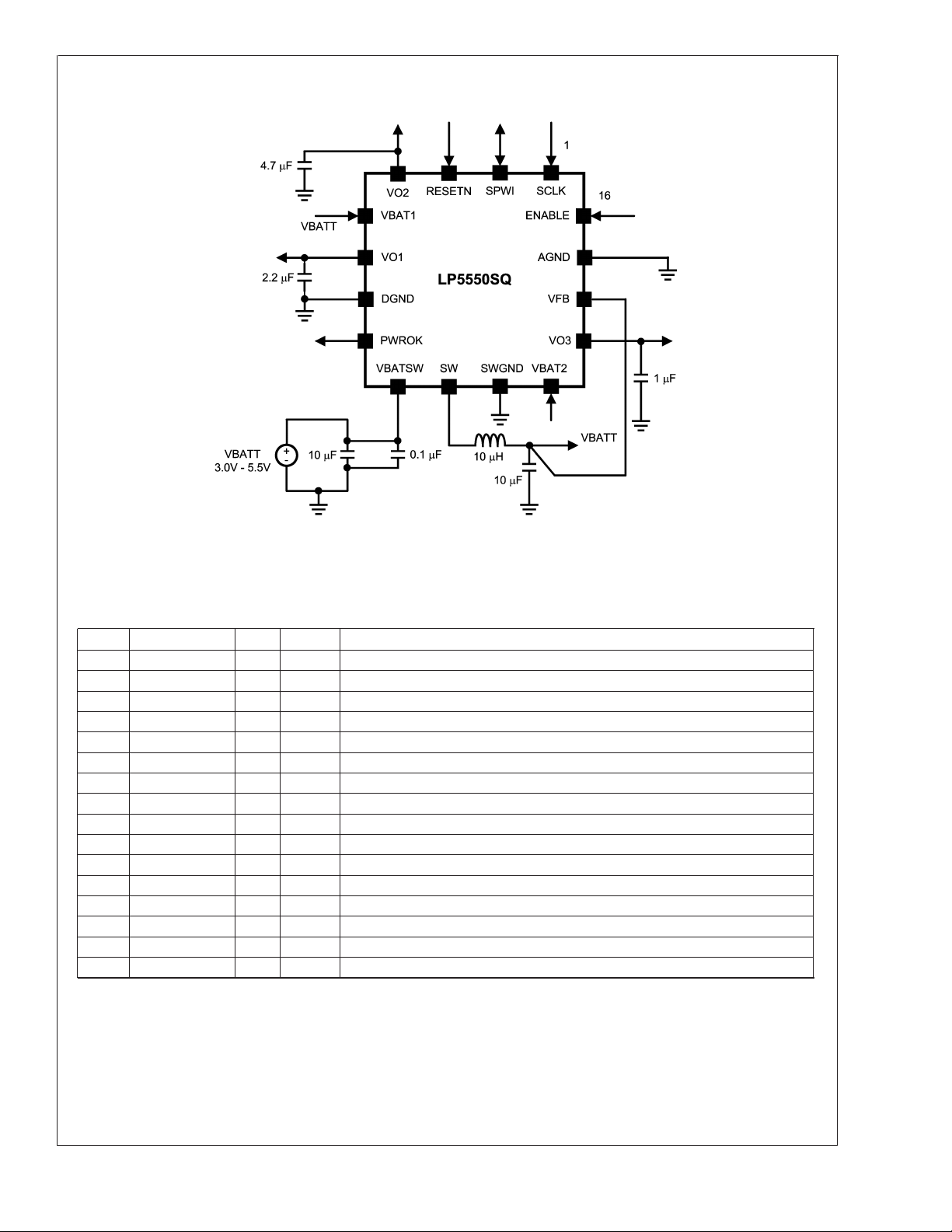
Typical Application
LP5550
20154530
FIGURE 4. Typical Application Circuit
Pin Descriptions
Pin # Name I/O Type Description
1 SCLK I D PowerWise Interface (PWI) clock input
2 SPWI I/O D PowerWise Interface (PWI) bi-directional data
3 RESETN I D Reset, active low
4 VO2 O A LDO2 output, for supplying the I/O voltage on the SoC
5 VBAT1 P P Battery supply voltage
6 VO1 O A LDO1 output, for supplying a fixed voltage to a PLL etc. on the SoC
7 DGND G G Digital ground
8 PWROK O D Power OK, active high output signal
9 VBATSW P P Battery supply voltage for switching regulator
10 SW O A Switcher pin connected to coil
11 SWGND G G Switcher ground
12 VBAT2 P P Battery supply voltage
13 VO3 O A LDO3 output, on-chip memory supply voltage
14 VFB I A Switcher output voltage for supplying SoC core logic
15 AGND G G Analog Ground
16 ENABLE I D Enable, active high
A: Analog Pin
D: Digital Pin
I: Input Pin
O: Output Pin
I/O: Input/Output Pin
P: Power Pin
G: Ground Pin
www.national.com3

Ordering Information
LP5550
Voltage Option Order Number Package Marking Supplied As
LP5550SQ LP5550SQ 1000 units, Tape-and-Reel
LP5550SQX LP5550SQ 4500 units, Tape-and-Reel
*Released. Samples available.
www.national.com 4

LP5550
Absolute Maximum Ratings (Notes 1, 2)
If Military/Aerospace specified devices are required,
please contact the National Semiconductor Sales Office/
Distributors for availability and specifications.
ESD Rating (Note 3)
Human Body Model:
SW pin 1.0kV
All other pins 2.0kV
VBAT1, VBAT2, VBATSW -0.3 to +6.0V
VO1, VO2, VO3 to GND -0.3 to +VBAT1+0.3V
Operating Ratings (Notes 1, 2)
ENABLE, RESETN, VFB,
SW,
SPWI, SCLK, PWROK -0.3 to VBAT2+0.3V
±
DGND, AGND, SWGND to
0.3V
GND SLUG
VBAT1, VBAT2, VBATSW 3.0V to 5.5V
Junction Temperature (T
)
J
−40˚C to +125˚C
Range
Ambient Temperature (T
)
A
−40˚C to +85˚C
Range(Note 5)
Junction Temperature
(TJ-MAX)
Storage Temperature Range -65˚C to 150˚C
Maximum Continuous
Power Dissipation
150˚C
1.0 W
Thermal Properties(Note 6)
Junction-to-Ambient
Thermal Resistance (θ
)
JA
39.8˚C/W
(PD-MAX) (Note 3)
Maximum Lead
Note 4
Temperature (Soldering)
General Electrical Characteristics Unless otherwise noted, V
BAT1,2,SW
, RESETN, ENABLE = 3.6V.
Typical values and limits appearing in normal type apply for TJ = 25˚C. Limits appearing in boldface type apply over the entire
junction temperature range for operation, -40 to +125˚C. (Notes 2, 7, 8, 9)
Symbol Parameter Conditions Min Typ Max Units
I
Q
T
SD
Shutdown Supply current V
Sleep State Supply Current
load 1 mA)
(V
O3
Acitve State Supply Current
(No load, PFM mode)
BAT1,2,SW
V
BAT1,2,SW
PWI on. All other circuits off.
V
BAT1,2,SW
Switcher on, PWI on.
= 2.0V, all circuits off. 1 6 µA
= 3.6V, LDO3 (VO3) on,
= 3.6V, LDOs 1 and 2 on,
70 85 µA
140 165 µA
Thermal Shutdown Threshold 160 ˚C
Thermal Shutdown Hysteresis 10
LDO1 (PLL/Fixed Voltage) Characteristics Unless otherwise noted, V
BAT1,2,SW
, RESETN, ENABLE = 3.6V. Typical values and limits appearing in normal type apply for TJ = 25˚C. Limits appearing in boldface type apply
over the entire junction temperature range for operation, -40 to +125˚C. (Notes 2, 7, 8)
Symbol Parameter Conditions Min Typ Max Units
V
OUT
Accuracy
V
Range Programmable Output Voltage
OUT
I
OUT
I
Q
∆V
OUT
Output Voltage 1mA ≤ IOUT ≤ 100mA,V
≤ 5.5V
≤ 100mA, Programming
Range
3.0V ≤ V
0µA ≤ I
BAT1,2,SW
OUT
Resolution=100mV
OUT
= 2V,
-3% 2 3% V
0.7 1.2 2.2 V
Recommended Output Current 3.0V ≤ VBAT1,2,SW ≤ 5.5V 100 mA
Short Circuit Current Limit V
Quiescent Current I
Line Regulation 3.0V ≤ V
=0V 350
OUT
= 0mA(Note 11) 35 45 µA
OUT
BAT1,2,SW
≤ 5.5V, I
OUT
=
-0.0125 0.0125 %/V
50mA
Load Regulation VIN= 3.6V, 1mA ≤ I
Line Transient Regulation 3.6V ≤ V
≤ 3.9V, TRISE,FALL = 10
IN
≤ 100mA -0.0085 0.0085 %/mA
OUT
27 mV
µs
Load Transient Regulation VIN= 3.6V, 10mA ≤ I
OUT
≤ 90 mA,
86 mV
TRISE,FALL = 100 ns
eN Output Noise Voltage 10Hz ≤ f ≤ 100kHz,C
= 2.2µF 0.103 mVRMS
OUT
www.national.com5
LDO1 (PLL/Fixed Voltage) Characteristics Unless otherwise noted, V
ENABLE = 3.6V. Typical values and limits appearing in normal type apply for TJ = 25˚C. Limits appearing in boldface type
LP5550
apply over the entire junction temperature range for operation, -40 to +125˚C. (Notes 2, 7, 8) (Continued)
BAT1,2,SW
, RESETN,
Symbol Parameter Conditions Min Typ Max Units
PSRR Power Supply Ripple Rejection
Ratio
C
OUT
Output CapacitanceOutput
Capacitor ESR
t
START-UP
Start-Up Time from Shut-down C
f = 1kHz,C
f = 10kHz,C
0µA ≤ I
OUT
= 1µF, I
OUT
= 2.2µF 56 dB
OUT
= 2.2µF 36 dB
OUT
≤ 100mA 1 2.2 20 µF
5 500 mΩ
= 100mA 54 µs
OUT
LDO2 (I/O Voltage) Characteristics Unless otherwise noted, V
BAT1,2,SW
, RESETN, ENABLE = 3.6V.
Typical values and limits appearing in normal type apply for TJ = 25˚C. Limits appearing in boldface type apply over the entire
junction temperature range for operation, -40 to +125˚C. (Notes 2, 7, 8)
Symbol Parameter Conditions Min Typ Max Units
V
OUT
Output Voltage 1mA ≤ I
Accuracy
V
Range Programmable Output Voltage
OUT
Range
V
OUT
0µA ≤ I
≤ 250mA,V
OUT
+0.4V ≤ V
OUT
BAT1,2,SW
≤ 250mA, 1.5-2.3V
OUT
= 3.3V,
≤ 5.5V
=100mV step, 2.5V, 2.8V, 3.0V and
-3% 3.3 3% V
1.5 3.3 3.3 V
3.3V
I
OUT
Recommended Output Current V
Output Current Limit V
Dropout Voltage(Note 10) I
I
Q
∆V
OUT
Quiescent Current I
Line Regulation V
Load Regulation V
Line Transient Regulation 3.6V ≤ V
Load Transient Regulation V
eN Output Noise Voltage 10Hz ≤ f ≤ 100kHz,C
PSRR Power Supply Ripple Rejection
Ratio
C
OUT
Output Capacitance 0µA ≤ I
+0.4V ≤ V
OUT
=0V 740
OUT
= 125mA 70 260 mV
OUT
= 0mA (Note 11) 55 60 µA
OUT
+0.4V ≤ V
OUT
= 125mA
I
OUT
= 3.6V, 1mA ≤ I
IN
= 3.6V, 25mA ≤ I
IN
T
RISE,FALL
f = 1kHz, C
f = 10kHz, C
OUT
BAT1,2,SW
BAT1,2,SW
≤ 3.9V, T
IN
= 100 ns
= 4.7µF 46 dB
OUT
= 4.7µF 34
OUT
≤ 250mA 2 4.7 20 µF
≤ 5.5V 250 mA
≤ 5.5V,
≤ 250mA -0.011 0.011 %/mA
OUT
RISE,FALL
OUT
OUT
=10us 24 mV
≤ 225 mA,
= 4.7µF 0.120 mVRMS
-0.0125 0.0125 %/V
246 mV
Output Capacitor ESR 5 500 mΩ
t
START-UP
Start-Up Time from Shut-down C
OUT
= 4.7µF, I
= 250mA 144 µs
OUT
LDO3 (Memory Retention Voltage) Characteristics Unless otherwise noted, V
BAT1,2,SW
RESETN, ENABLE = 3.6V. Typical values and limits appearing in normal type apply for TJ = 25˚C. Limits appearing in boldface type apply over the entire junction temperature range for operation, -40 to +125˚C. (Notes 2, 7, 8)
Symbol Parameter Conditions Min Typ Max Units
V
OUT
Accuracy
V
OFFSET
V
Range Programmable Output Voltage
OUT
I
Q
www.national.com 6
Output Voltage Active state:
Tracking V
AVS
Sleep state: Memory retention
voltage regulation
Active State Buffer offset (=
O3-VFB
)
V
Range (Sleep state)
I
≤ 50mA,VOUT = 1.2V, 3.0V ≤
OUT
V
BAT1,2,SW
I
OUT
V
BAT1,2,SW
I
OUT
V
OUT
I
OUT
V
OUT
0µA ≤ I
≤ 5.5V
≤ 5mA,V
≤ 5.5V
=50mA,
= 0.6 V
=50mA,
= 1.2V
≤ 5mA, Programming
OUT
Resolution=50mV
Quiescent Current Active mode, I
Sleep mode, I
-3% 1.2 3% V
= 1.2V, 3.0V ≤
OUT
-3% 1.2 3% V
13 mV
28 mV
0.6 1.2 1.35 V
= 10µA (Note 11) 33 44 µA
OUT
= 10µA (Note 11) 10 16 µA
OUT
,

LP5550
LDO3 (Memory Retention Voltage) Characteristics Unless otherwise noted, V
BAT1,2,SW
,
RESETN, ENABLE = 3.6V. Typical values and limits appearing in normal type apply for TJ = 25˚C. Limits appearing in
boldface type apply over the entire junction temperature range for operation, -40 to +125˚C. (Notes 2, 7, 8) (Continued)
Symbol Parameter Conditions Min Typ Max Units
I
OUT
Recommended Output Current,
3.0V ≤ V
BAT1,2,SW
≤ 5.5V 50 mA
Active state
Recommended Output Current,
3.0V ≤ V
BAT1,2,SW
≤ 5.5V 5
Sleep state
Short Circuit Current Limit,
V
=0V 230
OUT
Active state
eN Output Voltage Noise 10Hz ≤ f ≤ 100kHz,C
PSRR Power Supply Ripple Rejection
f = 217Hz, C
= 1.0µF 36 dB
OUT
= 1µF 0.158 mVRMS
OUT
Ratio
COUT Output Capacitance 0µA ≤ I
≤ 5mA 0.7 1 2.2 µF
OUT
Output Capacitor ESR 5 500 mΩ
Switcher (Core Voltage) Characteristics Unless otherwise noted, V
BAT1,2,SW
, RESETN, ENABLE
= 3.6V. Typical values and limits appearing in normal type apply for TJ = 25˚C. Limits appearing in boldface type apply over
the entire junction temperature range for operation, -40 to +125˚C. (Notes 2, 7, 8)
Symbol Parameter Conditions Min Typ Max Units
BAT1,2,SW
<
1.53% 2.70% V
-0.44% 2.70%
0.6 1.2 1.2 V
0.0019 %/mA
0.18 %/V
V
OUT
Output Voltage I
Accuracy
V
Range Programmable Output Voltage
OUT
Range
∆V
OUT
Line regulation 3.0V<V
Load regulation V
I
Q
R
DSON(P)
R
DSON(N)
I
LIM
f
OSC
C
OUT
Quiescent current consumption I
P-FET resistance V
N-FET resistance V
Switch peak current limit 3.0V<V
Internal oscillator frequency PWM-mode 800 1000 1360 kHz
Output Capacitance 0mA ≤ I
= 1 mA, V
OUT
V
BAT1,2,SW
I
OUT
<
5.5V
0mA ≤ I
<
= 1-300 mA, 3.0V<V
OUT
= 1.2V, 3.0V
OUT
5.5V
≤ 300mA, Programming
Resolution = 4.7mV
<
BAT1,2,SW
=10mA
I
OUT
BAT1,2,SW
I
OUT
OUT
BAT1,2,SW
BAT1,2,SW
= 3.6V
= 100-300mA
= 0mA 15 30 µA
= VGS = 3.6V 360 690 mΩ
= VGS = 3.6V 250 660 mΩ
BAT1,2,SW
≤ 300mA 5 10 22 µF
OUT
5.5V,
<
5.5V 400 620 750 mA
Output Capacitor ESR 5 500 mΩ
L Inductor inductance 0uA ≤ I
R
VFB
VFBpin resistance to ground 150 650 kΩ
≤ 300mA 4.7 / 10 µH
OUT
Logic and Control Inputs Unless otherwise noted, V
BAT1,2,SW
, RESETN, ENABLE = 3.6V. Typical values
and limits appearing in normal type apply for TJ = 25˚C. Limits appearing in boldface type apply over the entire junction temperature range for operation, -40 to +125˚C. (Notes 2, 7, 8, 9)
Symbol Parameter Conditions Min Typ Max Units
V
IL
V
IH
Input Low Level ENABLE, RESETN, SPWI, SCLK
3.0V ≤ V
Input High Level ENABLE, RESETN 3.0V ≤ V
BAT1
≤ 5.5V
BAT1
≤
2 V
0.2 V
5.5V
V
IH_PWI
I
IL
Input High Level, PWI SPWI, SCLK, 1.5V ≤VO2≤ 3.3V VO2-0.2V V
Logic Input Current ENABLE, RESETN, 0V ≤ V
BAT1
≤
-5 5 µA
5.5V
I
IL_PWI
Logic Input Current, PWI SPWI, SCLK, 1.5V ≤ VO2≤ 3.3V -5 15 µA
www.national.com7

Logic and Control Inputs Unless otherwise noted, V
and limits appearing in normal type apply for TJ = 25˚C. Limits appearing in boldface type apply over the entire junction
LP5550
temperature range for operation, -40 to +125˚C. (Notes 2, 7, 8, 9) (Continued)
BAT1,2,SW
, RESETN, ENABLE = 3.6V. Typical values
Symbol Parameter Conditions Min Typ Max Units
R
PD_PWI
Pull-down resistance for PWI
0.5 1 2 MΩ
signals
T
EN_LOW
Minimum low pulse width to
enter STARTUP state
ENABLE pulsed high - low - high
from SHUTDOWN state
ENABLE pulsed high - low - high
100 µsec
4
from SLEEP or ACTIVE state
Logic and Control Outputs Unless otherwise noted, V
BAT1,2,SW
, RESETN, ENABLE = 3.6V. Typical values and limits appearing in normal type apply for TJ = 25˚C. Limits appearing in boldface type apply over the entire junction
temperature range for operation, -40 to +125˚C. (Notes 2, 7, 8, 9)
Symbol Parameter Conditions Min Typ Max Units
V
OL
V
OH
V
OH_PWI
Note 1: Absolute Maximum Ratings indicate limits beyond which damage to the component may occur. Operating Ratings are conditions under which operation of
the device is guaranteed. Operating Ratings do not imply guaranteed performance limits. For guaranteed performance limits and associated test conditions, see the
Electrical Characteristics tables.
Note 2: All voltages are with respect to the potential at the GND pin.
Note 3: The Human body model is a 100 pF capacitor discharged through a 1.5 kΩ resistor into each pin.
The amount of Absolute Maximum power dissipation allowed for the device depends on the ambient temperature and can be calculated using the formula P = (TJ
– TA)/θ
, (1) where TJ is the junction temperature, TA is the ambient temperature, and JA is the junction-to-ambient thermal resistance.
JA
Junction-to-ambient thermal resistance is highly application and board-layout dependent. In applications where high maximum power dissipation exists, special care
must be paid to thermal dissipation issues in board design.
Internal thermal shutdown circuitry protects the device from permanent damage. Thermal shutdown engages at TJ=150˚C (typ.) and disengages at TJ=140˚C (typ.).
Note 4: For detailed soldering specifications and information, please refer to National Semiconductor Application Note 1187: Leadless Leadframe Package (LLP)
(AN-1187).
Note 5: In applications where high power dissipation and/or poor package thermal resistance is present, the maximum ambient temperature may have to be
derated. Maximum ambient temperature (TA-MAX) is dependent on the maximum operating junction temperature (TJ-MAX-OP = 125˚C), the maximum power
dissipation of the device in the application (PD-MAX), and the junction-to ambient thermal resistance of the part/package in the application (θ
following equation: TA-MAX = TJ-MAX-OP – (θJA x PD-MAX).
Note 6: Junction-to-ambient thermal resistance (θJA) is taken from a thermal modeling result, performed under the conditions and guidelines set forth in the JEDEC
standard JESD51-7. The test board is a 4-layer FR-4 board measuring 102mm x 76mm x 1.6mm with a 2x1 array of thermal vias. The ground plane on the board
is 50mm x 50mm. Thickness of copper layers are 36µm/18µm/18µm/36µm (1.5oz/1oz/1oz/1.5oz). Ambient temperature in simulation is 22˚C, still air. Power
dissipation is 1W.
Junction-to-ambient thermal resistance is highly application and board-layout dependent. In applications where high maximum power dissipation exists, special care
must be paid to thermal dissipation issues in board design.
The value of θ
dissipation exists (high VIN, high IOUT), special care must be paid to thermal dissipation issues. For more information on these topics, please refer to Application
Note 1187: Leadless Leadframe Package (LLP) and the Power Efficiency and Power Dissipation section of this datasheet.
Note 7: All limits are guaranteed by design, test and/or statistical analysis. All electrical characteristics having room-temperature limits are tested during production
with TJ = 25C. All hot and cold limits are guaranteed by correlating the electrical characteristics to process and temperature variations and applying statistical process
control.
Note 8: Capacitors: Low-ESR Surface-Mount Ceramic Capacitors are (MLCCs) used in setting electrical characteristics
Note 9: Guaranteed by design.
Note 10: Dropout voltage is the input-to-output voltage difference at which the output voltage is 100mV below its nominal value. This specification does not apply
in cases it implies operation with an input voltage below the 3.0V minimum appearing under Operating Ratings. For example, this specification does not apply for
devices having 1.5V outputs because the specification would imply operation with an input voltage at or about 1.5V
Note 11: Quiescent current for LDO1, LDO2, and LDO3 do not include shared functional blocks such as the bandgap reference.
Output low level PWROK, SPWI, I
Output high level PWROK, I
Output high level, PWI SPWI, I
of this product can vary significantly, depending on PCB material, layout, and environmental conditions. In applications where high maximum power
JA
SOURCE
SOURCE
≤ 1mA 0.4 V
SINK
≤ 1mA V
-0.4V V
BAT1
≤ 1mA VO2-0.4V V
), as given by the
JA
www.national.com 8

Simplified Functional Diagram
LP5550
FIGURE 5. Simplified Functional Diagram
20154532
www.national.com9

Typical Performance Characteristics Unless otherwise stated: V
LP5550
Sleep, no load on LDO3
I
Q
vs. V
IN
20154504 20154505
=3.6V
IN
I
vs. V
Q
Shutdown
IN
Start-up Sequence
V
O1,VO2,VOSW
Start-up Sequence
Inrush Current
Start-up Sequence
V
OSW,VO3
20154506 20154507
Line Transient Response
V
OSW,VO3
20154556 20154509
www.national.com 10

LP5550
Typical Performance Characteristics Unless otherwise stated: V
Line Transient Response
V
O1,VO2
Load Transient Resoponse
V
O1
20154553 20154554
Load Transient Response
=3.6V (Continued)
IN
V
O2
LDO1 PSRR
20154555
LDO2 PSRR LDO3 PSRR
20154558 20154559
20154557
www.national.com11

Typical Performance Characteristics Unless otherwise stated: V
LP5550
Switching Frequency vs. V
Load Trainsiet Response
Switcher, PWM only
IN
20154510
Switcher, Automatic PWM/PFM Transition
=3.6V (Continued)
IN
Load Transient Response
Load Transient Response
Switcher, PFM only
20154513
20154514 20154515
V
Transient Response
OUT
Min to Max Transient
20154516 20154517
www.national.com 12
V
Transient Response
OUT
Max to Min Transient

LP5550
Typical Performance Characteristics Unless otherwise stated: V
Switch Current Limit vs. V
Switching Waveforms
PWM
IN
20154518
Efficiency vs. Load (Switcher)
Switching Waveforms
=3.6V (Continued)
IN
PFM
20154519
20154520 20154521
LP5550 PWI Register Map
The PWI standard supports sixteen 8-bit registers on the PWI slave. The table below summarizes these registers and shows
default register bit values after reset. The following sub-sections provide additional detail on the use of each individual register.
Summary
Register
Address
Register
Name Register Usage Type
0x0 R0 Core voltage R/W 0111 1 11 1
0x1 R1 Unused R/W ---- - -- -
0x2 R2 Memory retention voltage R/W 0110 0 - - -
0x3 R3 Status register R/O 0000 1 11 1
0x4 R4 PWI version number R/O 0000 0 00 1
0x5 R5 Unused R/W ---- - -- -
0x6 R6 Unused R/W ---- - -- -
0x7 R7 LDO2 voltage R/W 0111 1 - - -
0x8 R8 LDO1 voltage R/W 0010 1 - - -
0x9 R9 PFM/PWM force R/W 0 0 - - - - - -
Reset Default Value
7654 3 21 0
www.national.com13

LP5550 PWI Register Map (Continued)
LP5550
Summary (Continued)
Register
Address
0xA R10 Unused R/W ---- - -- -
0xB R11 Unused R/W ---- - -- -
0xC R12 Unused R/W ---- - -- -
0xD R13 Unused R/W ---- - -- -
0xE R14 Unused R/W ---- - -- -
0xF R15 Reserved R/W ---- - -- -
Register
Name Register Usage Type
Reset Default Value
7654 3 21 0
R0 - Core Voltage Register
Address 0x0
Type R/W
Reset Default 8h’7F
Bit Field Name Description or Comment
7 Sign This bit is fixed to ‘0’. Reading this bit will result in a ‘0’. Any data written into
this bit position using the Register Write command is ignored.
6:0 Voltage Core voltage value. Default value is in bold.
Voltage Data Code [7:0] Voltage Value (V)
7h’00 0.6
7h’xx Linear scaling
7h’7f 1.2 (default)
R1 - Unused Register
Address 0x1
Type R/W
Reset Default 8h’00
Bit Field Name Description or Comment
7:0 Unused Write transactions to this register are ignored. Read transactions will
return a “No Response Frame.” A no response frame contains all
zeros (see PWI 1.0 specification).
R2 – VO3 Voltage Register (Memory Retention Voltage)
Address 0x2
Type R/W
Reset Default 8h’60
Bit Field Name Description or Comment
7 Sign This bit is fixed to ‘0’. Reading this bit will result in a ‘0’. Any data written into
this bit position using the Register Write command is ignored.
www.national.com 14

R2 – VO3 Voltage Register (Memory Retention Voltage) (Continued)
Bit Field Name Description or Comment
6:3 Voltage Fixed voltage value. A code of all ones indicates maximum voltage while a code
of all zero indicates minimum voltage. Default value is in bold.
Voltage Data Code [6:3] Voltage Value (volts)
4h’0 0.6
4h’1 0.65
4h’2 0.7
4h’3 0.75
4h’4 0.8
4h’5 0.85
4h’6 0.9
4h’7 0.95
4h’8 1
4h’9 1.05
4h’A 1.1
4h’B 1.15
4h’C 1.20 (default)
4h’D 1.25
4h’E 1.3
4h’F 1.35
2:0 Unused These bits are fixed to ‘0’. Reading
these bits will result in a ‘000’. Any data
written into these bits using the
Register Write command is ignored.
LP5550
R3 - Status Register
Address 0x3
Type Read Only
Reset Default 8h’0F
Bit Field Name Description or Comment
7 Reserved Reserved, read returns 0
6 Reserved Reserved, read returns 0
5 User Bit Unused, read returns 0
4 User Bit Unused, read returns 0
3 Fixed OK Unused, read returns 1
2 IO OK Unused, read returns 1
1 Memory OK Unused, read returns 1
0 Core OK Unused, read returns 1
R4 - PWI Version Number Register
Address 0x4
Type Read Only
Reset Default 8h’01
Bit Field Name Description or Comment
7:0 Version Read transaction will return 8h’01 indicating PWI 1.0 specification.
Write transactions to this register are ignored.
www.national.com15

R5-R6 - Unused Registers
Address 0x5, 0x6
LP5550
Type R/W
Reset Default 8h’00
Bit Field Name Description or Comment
7:00 Unused Write transactions to this register are ignored. Read transactions will
return a “No Response Frame.” A no response frame contains all
zeros (see PWI 1.0 specification).
R7 – VO2 Voltage Register (I/O Voltage)
Address 0x7
Type R/W
Reset Default 8h’78
Bit Field Name Description or Comment
7 Sign This bit is fixed to ‘0’. Reading this bit will result in a ‘0’. Any data written into
this bit position using the Register Write command is ignored.
6:3 Voltage Fixed voltage value. A code of all ones indicates maximum voltage while a code
of all zero indicates minimum voltage. Default value is in bold.
Voltage Data Code [6:3] Voltage Value (volts)
4h’0 1.5
4h’1 1.5
4h’2 1.5
4h’3 1.5
4h’4 1.6
4h’5 1.7
4h’6 1.8
4h’7 1.9
4h’8 2
4h’9 2.1
4h’A 2.2
4h’B 2.3
4h’C 2.5
4h’D 2.8
4h’E 3
4h’F 3.3 (default)
2:0 Unused These bits are fixed to ‘0’. Reading these bits will result in a ‘000’. Any data
written into these bits using the Register Write command is ignored.
R8 – VO1 Voltage Register (PLL/Fixed Voltage)
Address 0x8
Type R/W
Reset Default 8h’28
Bit Field Name Description or Comment
7 Sign This bit is fixed to ‘0’. Reading this bit will result in a ’0’. Any data written into
this bit position using the Register Write command is ignored.
www.national.com 16

R8 – VO1 Voltage Register (PLL/Fixed Voltage) (Continued)
Bit Field Name Description or Comment
6:3 Voltage Fixed voltage value. A code of all ones indicates maximum voltage while a code
of all zero indicates minimum voltage. Default value is in bold.
Voltage Data Code [6:3] Voltage Value (volts)
4h’0 0.7
4h’1 0.8
4h’2 0.9
4h’3 1
4h’4 1.1
4h’5 1.2 (default)
4h’6 1.3
4h’7 1.4
4h’8 1.5
4h’9 1.6
4h’A 1.7
4h’B 1.8
4h’C 1.9
4h’D 2
4h’E 2.1
4h’F 2.2
2:0 Unused These bits are fixed to ‘0’. Reading these bits will result in a 3b’000. Any data
written into these bits using the Register Write command is ignored.
LP5550
R9– PFM/PWM Force Register
Address 0x9
Type R/W
Reset Default 8h’00
Bit Field Name Description or Comment
7:6 PFM/PWM
Force
Automatic Transition 0 0
Automatic Transition 1 1
Forced PFM Mode 1 0
Forced PWM Mode 0 1
5:0 Unused These bits are fixed to ‘0’. Reading these bits will result in a ‘000000’. Any data written into
these bits using the Register Write command is ignored.
User Register
PFM Force (bit 7) PWM Force (bit 6)
R10-R14 – Unused Registers
Address 0xA, 0xB, 0xC, 0xD, 0xE
Type R/W
Reset Default 8h’00
Bit Field Name Description or Comment
7:0 Unused Write transactions to this register are ignored. Read transactions will
return a “No Response Frame.” A no response frame contains all
zeros (see PWI 1.0 specification) frame.
www.national.com17

R15 – Manufacturer Register
Adress 0xF
LP5550
Type R/W
Bit Field Name Description or Comment
7:0 Reserved Do not write to this register
Reset Default 8h’00
www.national.com 18

Operation Description
DEVICE INFORMATION
The LP5550 is a PowerWise Interface (PWI) compliant
power management unit (PMU) for application or baseband
processors in mobile phones or other portable equipment. It
operates cooperatively with processors using National Semiconductor’s Advanced Power Controller (APC) to provide
Adaptive or Dynamic Voltage Scaling (AVS, DVS) which
drastically improves processor efficiencies compared to conventional power delivery methods. The LP5550 consists of a
high efficiency switching DC/DC buck converter to supply the
AVS or DVS voltage domain, three LDOs for supplying the
logic, PLL, and memory, and PWI registers and logic.
OPERATION STATE DIAGRAM
The LP5550 has four operating states: Start-up, Active,
Sleep and Standby.
The Start-up state is the default state after reset. All regulators are off and PWROK output is ‘0’. The device will power
up when the external enable-input is pulled high. After the
power-up sequence LP5550 enters the Active state.
In the Active state all regulators are on and PWROK-output
is ‘1’. Immediately after Start-up the output voltages are at
LP5550
their default levels. LP5550 can be turned off by supplying
the Shutdown command over PWI, or by setting ENABLE
and/or RESETN to ’0’. The LP5550 can be switched to the
Sleep state by issuing the Sleep command.
In the Sleep state the core voltage regulator is off, but the
PWROK output is still ‘1’. The memory voltage regulator
(VO3) provides the programmed memory retention voltage.
LDO1 and LDO2 are on. The LP5550 can be activated from
the Sleep state by giving the Wake-up command. This resumes the last programmed Active state configuration. The
device can also be switched off by giving the Shutdown
command, or by setting ENABLE and/or RESETN to ‘0’
In the Shutdown-state all output voltages are ‘0’, and
PWROK-signal is ‘0’ as well. The LP5550 can exit the
Shutdown-state if either ENABLE or RESETN is ‘0’. In either
case the device moves to the Start-up state. See the ENABLE
Figure 6 shows the LP5550 state diagram. The figure assumes that supply voltage to the regulator IC is in the valid
range.
FIGURE 6. LP5550 State Diagram
20154545
www.national.com19

Operation Description (Continued)
LP5550
VOLTAGE SCALING
The LP5550 is designed to be used in a voltage scaling
system to lower the power dissipation of baseband or application processors in mobile phones or other portable equipment. By scaling supply voltage with the clock frequency of a
processor, dramatic power savings can be achieved. Two
types of voltage scaling are supported, dynamic voltage
scaling (DVS) and adaptive voltage scaling (AVS). DVS
systems switch between pre-characterized voltages which
are paired to clock frequencies used for frequency scaling in
the processor. AVS systems track the processor performance and optimize the supply voltage to the required performance. AVS is a closed loop system that provides process and temperature compensation such that for any given
processor, temperature, or clock frequency, the minimum
supply voltage is delivered.
DIGITALLY CONTROLLED VOLTAGE SCALING
The LP5550 delivers fast, controlled voltage scaling transients with the help of a digital state machine. The state
machine automatically optimizes the control loop in the
LP5550 switching regulator to provide large signal transients
with minimal over- and undershoot. This is an important
characteristic for voltage scaling systems that rely on minimal over- and undershoot to set voltages as low as possible
and save energy.
LARGE SIGNAL TRANSIENT RESPONSE
The switching converter in the LP5550 is designed to work in
a voltage scaling system. This requires that the converter
has a well controlled large signal transient response. Specifically, the under- and over-shoots have to be minimal or
zero while maintaining settling times less than 100 usec.
Typical response plots are shown in the Typical Performance
section.
PowerWise (TM) INTERFACE
To support DVS and AVS, the LP5550 is programmable via
the low power, 2 wire PowerWise Interface (PWI). This serial
interface controls the various voltages and states of all the
regulators in the LP5550. In particular, the switching regulator voltage can be controlled between 0.6V and 1.2V in 128
steps (linear scaling). This high resolution voltage control
affords accurate temperature and process compensation in
AVS. The LDO voltages can also be set, however they are
not intended to be dynamic in operation. The LP5550 supports the full command set as described in PWI 1.0 specification:
Core Voltage Adjust
•
Reset
•
Sleep
•
Shutdown
•
Wakeup
•
Register Read
•
Register Write
•
Authenticate
•
Synchronize
•
PWM/PFM OPERATION
The switching converter in the LP5550 has two modes of
operation: pulse width modulation (PWM) and pulse frequency modulation (PFM). In PWM the converter switches at
1MHz. Each period can be split into two cycles. During the
first cycle, the high-side switch is on and the low-side switch
is off, therefore the inductor current is rising. In the second
cycle, the high-side switch is off and the low-side switch is on
causing the inductor current to decrease. The output ripple
voltage is lowest in PWM mode Figure 7. As the load current
decreases, the converter efficiency becoms worse due to the
increased percentage of overhead current needed to operate in PWM mode. The LP5550 can operate in PFM mode to
increase efficiency at low loads.
By default, the part will automatically transition into PFM
mode when either of two conditions occurs for a duration of
32 or more clock cycles:
A. The inductor valley current goes below 0 A
B. The peak PMOS switch current drops below the I
level:
During PFM operation, the converter positions the output
voltage slightly higher than the nominal output voltage during
PWM operation, allowing additional headroom for voltage
drop during a load transient from light to heavy load. The
PFM comparators sense the output voltage via the feedback
pin and control the switching of the output FETs such that the
output voltage ramps between 0.8% and 1.6% (typ) above
the nominal PWM output voltage. If the output voltage is
below the ‘high’ PFM comparator threshold, the PMOS
power switch is turned on. It remains on until the output
voltage exceeds the ‘high’ PFM threshold or the peak current
exceeds the I
in PFM mode is:
level set for PFM mode. The peak current
PFM
MODE
www.national.com 20

Operation Description (Continued)
LP5550
FIGURE 7. Operation in PFM Mode and Transfer to PWM Mode
20154503
www.national.com21

Application Information
LP5550
PWM/PFM FORCE REGISTER (R9)
By default, the LP5550 automatically transitions between
PFM and PWM to optimize efficiency. The PWM/PFM force
register (R9) provides the option to override the automatic
transition and force PFM or PWM operation (see R9 –
PWM/PFM Force Register declaration). Note that if the operating mode of the regulator is forced to be PFM then the
switch current limit is reduced to 100 mA (50 mA average
load current).
EN/RESETN
The LP5550 can be shutdown via the ENABLE or RESETN
pins, or by issuing a shutdown command from PWI. To
disable the LP5550 via hardware (as opposed to the PWI
shutdown command), pull the ENABLE and/or the RESETN
pin(s) low. To enable the LP5550, both the ENABLE and the
RESETN pins must be high. Once enabled, the LP5550
engages the power-up sequence and all voltages return to
their default values.
When using PWI to issue a shutdown command, the PWI will
be disabled along with the regulators in the LP5550. To
re-enable the part, either the ENABLE, RESETN, or both
pins must be toggled (high – low – high). The part will then
enter the power-up sequence and all voltages will return to
their default values. Figure 8 summarizes the ENABLE/
RESETN control.
The ENABLE and RESETN pins provide flexibility for system
control. In larger systems such as a mobile phone, it can be
advantageous to enable/disable a subsystem independently.
For example, the LP5550 may be powering the applications
processor in a mobile phone. The system controller can
power down the applications processor via the ENABLE pin,
but leave on other subsystems. When the phone is turned off
or in a fault condition, the system controller can have a
global reset command that is connected to all the subsystems (RESETN for the LP5550). However, if this type of
control is not needed, the ENABLE and RESETN pins can
be tied together and used as a single enable/disable pin.
INDUCTOR
A 10uH or 4.7uH inductor should be used with the LP5550.
The inductor should be rated to handle the peak load current
plus the ripple current:
CURRENT LIMIT
The switching converter in the LP5550 detects the peak
inductor current and limits it for protection (see Electrical
Characteristics table and/or Typical Performance section).
To determine the average current limit from the peak current
limit, the inductor size, input and output voltage, and switching frequency must be known. The LP5550 is designed to
work with a 4.7uH or 10uH inductor, so:
20154551
FIGURE 8. ENABLE and RESETN operation
www.national.com 22
INPUT CAPACITOR
The input capacitor to the switching converter supplies the
AC switching current drawn from the switching action of the
internal power FETs. The input current of a buck converter is
discontinuous, so the ripple current supplied by the input
capacitor is large. The input capacitor must be rated to
handle this current:
The power dissipated in the input capacitor is given by:
The input capacitor must be rated to handle both the RMS
current and the dissipated power. A 10 µF ceramic capacitor
is recommended for the LP5550.

Application Information (Continued)
OUTPUT CAPACITOR
The switching converter in the LP5550 is designed to be
used with a 10uF ceramic output capacitor. The dielectric
should be X5R, X7R, or comparable material to maintain
proper tolerances. The output capacitor of the switching
converter absorbs the AC ripple current from the inductor
and provides the initial response to a load transient. The
ripple voltage at the output of the converter is the product of
the ripple current flowing through the output capacitor and
the impedance of the capacitor. The impedance of the capacitor can be dominated by capacitive, resistive, or inductive elements within the capacitor, depending on the frequency of the ripple current. Ceramic capacitors are
predominately used in portable systems and have very low
ESR and remain capacitive up to high frequencies.
The switcher peak - to - peak output voltage ripple in steady
state can be calculated as:
TABLE 1. LDO Parameters
Output voltage
PWI Register
range
LDO1 R8 0.6 V – 2.2 V 100 mA 200 mV PLL
LDO2 R7 1.5 V – 3.3 V 250 mA 150 mV I/O
LDO3 R2 V
+ 0.05 V
OSW
0.7 V – 1.35 V
1
2
LDO INFORMATION
The LDOs included in the LP5550 provide static supply
voltages for various functions in the processor. Use the
following sections to determine loading and external components.
LDO LOADING CAPABILITY
The LDOs in the LP5550 can regulate to a variety of output
voltages, depending on the need of the processor. These
voltages can be programmed through the PWI. Table 1
summarizes the parameters of the LP5550 LDOs.
Recommended
Maximum Output
Current
Dropout Voltage
(typical) Typical Load
50 mA 200 mV Memory/Memory
retention
LP5550
1. LDO3 tracks the switching converter output voltage (V
) plus a 50 mV offset when the LP5550 is in active state.
OSW
2. LDO3 regulates at the set memory retention voltage when the LP5550 is in shutdown state.
LDO OUTPUT CAPACITOR
The output capacitor sets a low frequency pole and a high
frequency zero in the control loop of an LDO. The capacitance and the equivalent series resistance (ESR) of the
capacitor must be within a specified range to meet stability
requirements. The LDOs in the LP5550 are designed to be
used with ceramic output capacitors. The dielectric should
be X5R, X7R, or comparable material to maintain proper
tolerances. Use the following table to choose a suitable
output capacitor:
TABLE 2. Output Capacitor Selection Guide
Output Capacitance Range
(Recommended Typical Value) ESR range
LDO1 1 µF – 20 µF (2.2 µF) 5 mohm – 500 mohm
LDO2 2 µF – 20 µF (4.7 µF) 5 mohm – 500 mohm
LDO3 0.7 µF – 2.2 µF (1.0 µF) 5 mohm– 500 mohm
www.national.com23

Application Information (Continued)
LP5550
BOARD LAYOUT CONSIDERATIONS
FIGURE 9. Board Layout Design Recommendations for the LP5550
20154561
www.national.com 24

Physical Dimensions inches (millimeters) unless otherwise noted
LP5550 PowerWise
™
Technology Compliant Energy Management Unit
16-Lead LLP Package
NS Package Number SQA16A
National does not assume any responsibility for use of any circuitry described, no circuit patent licenses are implied and National reserves
the right at any time without notice to change said circuitry and specifications.
For the most current product information visit us at www.national.com.
LIFE SUPPORT POLICY
NATIONAL’S PRODUCTS ARE NOT AUTHORIZED FOR USE AS CRITICAL COMPONENTS IN LIFE SUPPORT DEVICES OR SYSTEMS
WITHOUT THE EXPRESS WRITTEN APPROVAL OF THE PRESIDENT AND GENERAL COUNSEL OF NATIONAL SEMICONDUCTOR
CORPORATION. As used herein:
1. Life support devices or systems are devices or systems
which, (a) are intended for surgical implant into the body, or
(b) support or sustain life, and whose failure to perform when
properly used in accordance with instructions for use
2. A critical component is any component of a life support
device or system whose failure to perform can be reasonably
expected to cause the failure of the life support device or
system, or to affect its safety or effectiveness.
provided in the labeling, can be reasonably expected to result
in a significant injury to the user.
BANNED SUBSTANCE COMPLIANCE
National Semiconductor manufactures products and uses packing materials that meet the provisions of the Customer Products
Stewardship Specification (CSP-9-111C2) and the Banned Substances and Materials of Interest Specification (CSP-9-111S2) and contain
no ‘‘Banned Substances’’ as defined in CSP-9-111S2.
Leadfree products are RoHS compliant.
National Semiconductor
Americas Customer
Support Center
Email: new.feedback@nsc.com
Tel: 1-800-272-9959
www.national.com
National Semiconductor
Europe Customer Support Center
Fax: +49 (0) 180-530 85 86
Email: europe.support@nsc.com
Deutsch Tel: +49 (0) 69 9508 6208
English Tel: +44 (0) 870 24 0 2171
Français Tel: +33 (0) 1 41 91 8790
National Semiconductor
Asia Pacific Customer
Support Center
Email: ap.support@nsc.com
National Semiconductor
Japan Customer Support Center
Fax: 81-3-5639-7507
Email: jpn.feedback@nsc.com
Tel: 81-3-5639-7560
 Loading...