National Semiconductor LP3999 Technical data

December 2003
LP3999
Low Noise 150mA Voltage Regulator for RF/Analog
Applications
LP3999 Low Noise 150mA Voltage Regulator for RF/Analog Applications
General Description
The LP3999 regulator is designed to meet the requirements
of portable wireless battery-powered applications and will
provide an accurate output voltage with low noise and low
quiescent current. Ideally suited for powering RF/Analog
devices this device will also be used to meet more general
circuit requirements.
For battery powered applications the low dropout and low
ground current provided by the device allows the lifetime of
the battery to be maximized.The inclusion of an Enable(disable) control can be used by the system to further extend the
battery lifetime by reducing the power consumption to virtually zero. Should the application require a device with an
active disable function please refer to device LP3995.
The LP3999 also features internal protection against shortcircuit currents and over-temperature conditions.
The LP3999 is designed to be stable with small 1.0 µF
ceramic capacitors. The small outline of the LP3999 micro
SMD package with the required ceramic capacitors can
realize a system application within minimal board area.
Performance is specified for a −40˚C to +125˚C temperature
range.
The device is available in micro SMD package and LLP
package. For other package options contact your local NSC
sales office.
The device is available in fixed output voltages in the ranges
of 1.5V to 3.3V. For availability, please contact your local
NSC sales office.
Key Specifications
n 2.5V to 6.0V Input Range
n Accurate Output Voltage;
n 60 mV Typical Dropout with 150 mA Load. V
n Virtually Zero Quiescent Current when Disabled
n 10 µVrms output noise over 10Hz to 100kHz
n Stable witha1µFOutput Capacitor
n Guaranteed 150 mA Output Current
n Fast Turn-on Time; 140 µs (Typ.)
±
75mV / 2%
>
2.5V
out
Features
n 5 pin micro SMD Package
n 6 pin LLP Package
n Stable with Ceramic Capacitor
n Logic Controlled Enable
n Fast Turn-on
n Thermal-overload and short-circuit protection
n −40 to +125˚C junction temperature range for operation
Applications
n GSM Portable Phones
n CDMA Cellular Handsets
n Wideband CDMA Cellular Handsets
n Bluetooth Devices
n Portable Information Appliances
n Handheld MP3 Devices
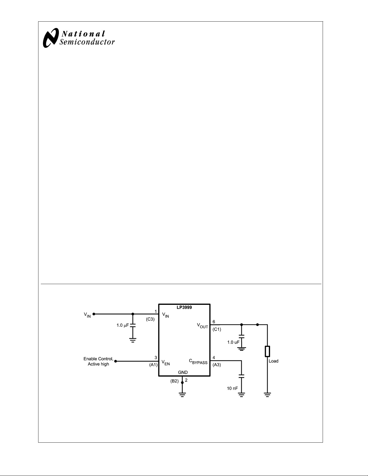
Typical Application Circuit
20052001
© 2003 National Semiconductor Corporation DS200520 www.national.com

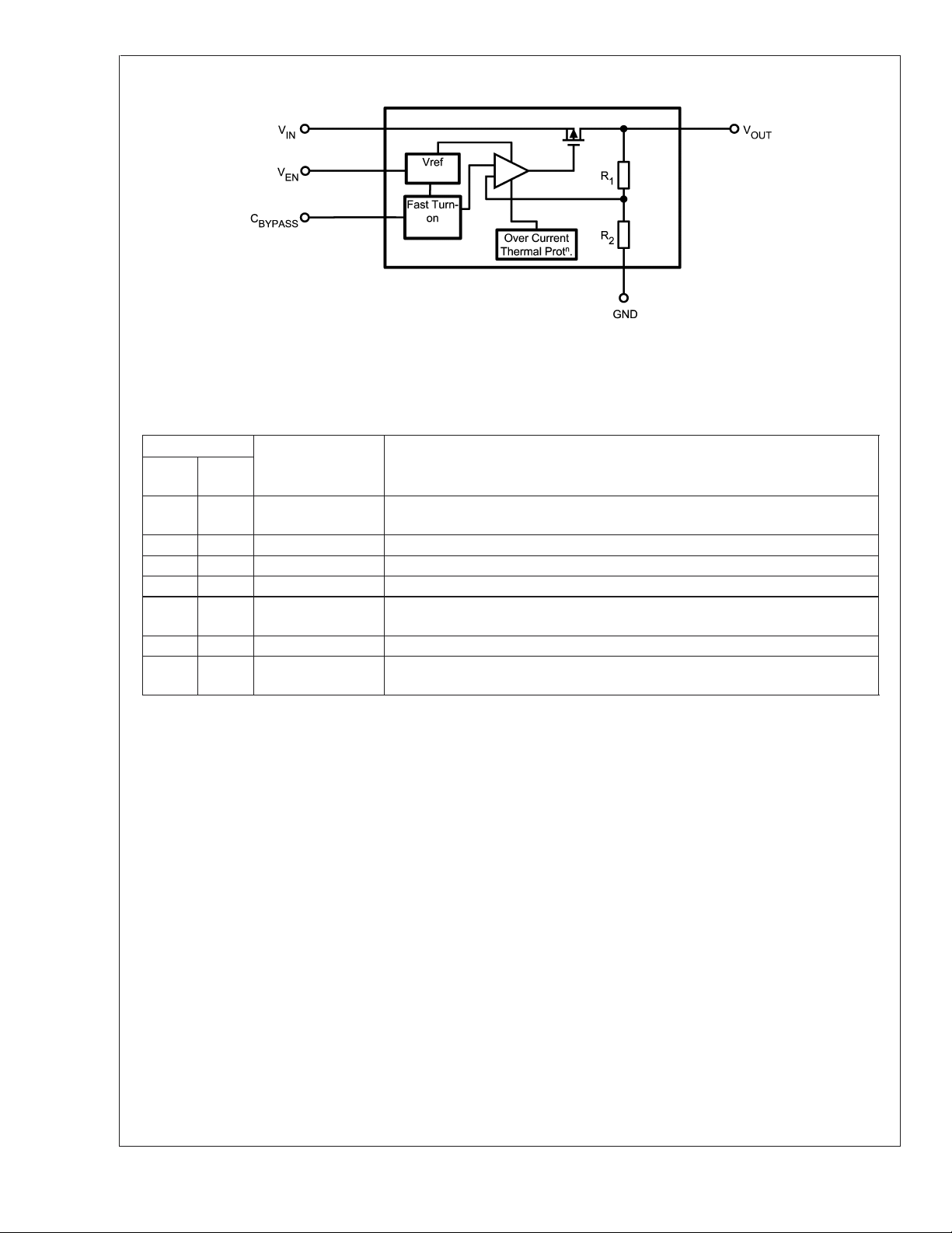
Block Diagram
LP3999
Pin Description
Package 5 pin micro SMD
Pin No. Symbol Name and Function
micro
SMD
A1 3 V
B2 2 GND Common Ground
C1 6 V
C3 1 V
A3 4 C
LLP
OUT
BYPASS
5 N/C No internal connection. There should not be any board connection to this pin.
Pad GND Ground connection.
20052002
EN
Enable Input; Disables the Regulator when ≤ 0.4V.
Enables the regulator when ≥ 0.9V
Voltage output. Connect this output to the load circuit.
IN
Voltage Supply Input
Bypass Capacitor connection.
Connect a 0.01 µF capacitor for noise reduction.
Connect to ground plane for best thermal conduction.
www.national.com 2

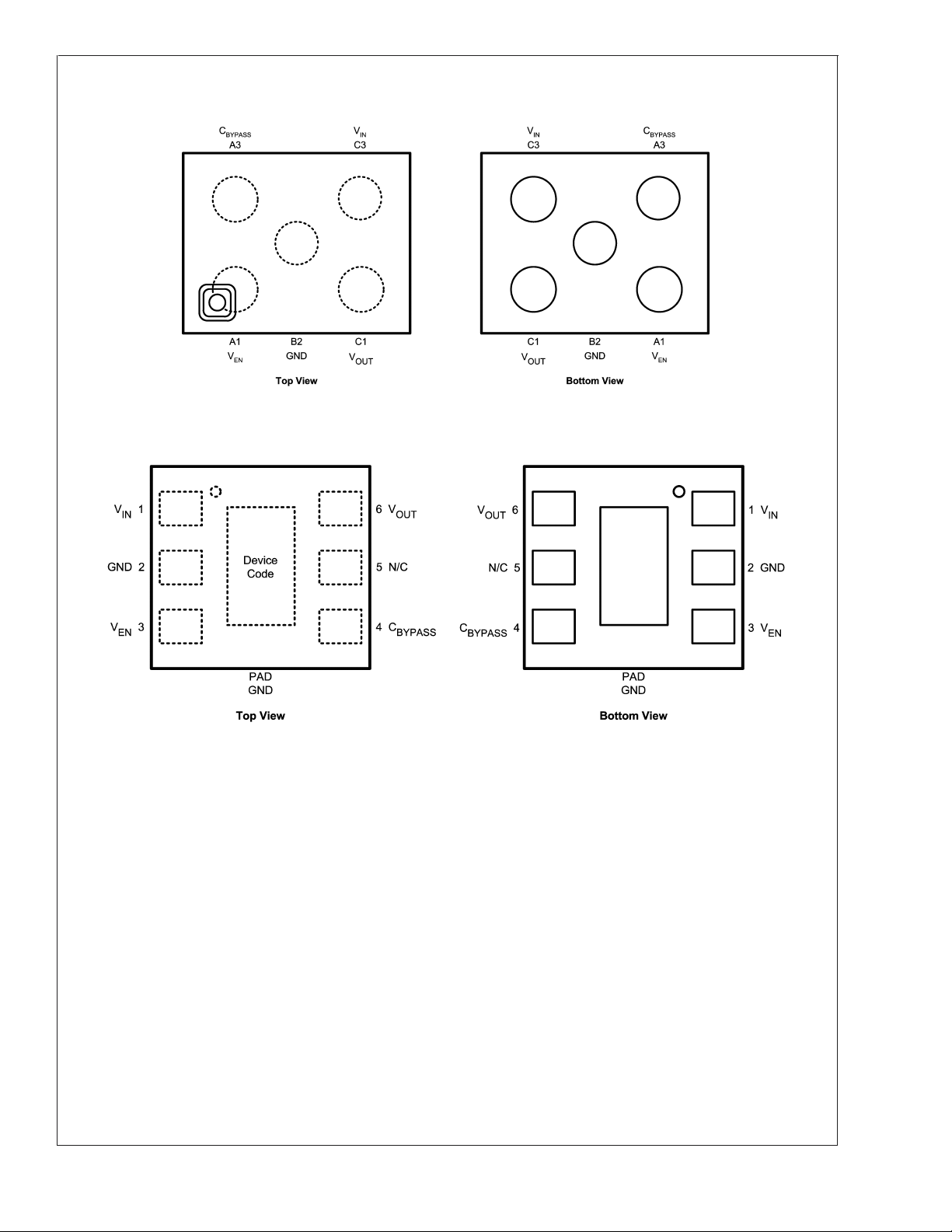
Connection Diagrams
LP3999
micro SMD, 5 Bump Package
See NS Package Number TLA05
LLP-6 Package (SOT23 footprint)
See NS Package Number LDE06A
20052003
20052004
www.national.com3

Ordering Information
LP3999
Output Voltage
(V)
1.5 STD LP3999ITL-1.5 LP3999ITLX-1.5
1.6 (Note 2) STD LP3999ITL-1.6 LP3999ITLX-1.6
1.7(Note 2) STD LP3999ITL-1.7 LP3999ITLX-1.7
1.8 STD LP3999ITL-1.8 LP3999ITLX-1.8
1.875 STD LP3999ITL-1.875 LP3999ITLX-1.875
1.9 (Note 2) STD LP3999ITL-1.9 LP3999ITLX-1.9
2.0(Note 2) STD LP3999ITL-2.0 LP3999ITLX-2.0
2.1 (Note 2) STD LP3999ITL-2.1 LP3999ITLX-2.1
2.2(Note 2) STD LP3999ITL-2.2 LP3999ITLX-2.2
2.4 STD LP3999ITL-2.4 LP3999ITLX-2.4
2.5 STD LP3999ITL-2.5 LP3999ITLX-2.5
2.6(Note 2) STD LP3999ITL-2.6 LP3999ITLX-2.6
2.8 STD LP3999ITL-2.8 LP3999ITLX-2.8
3.0(Note 2) STD LP3999ITL-3.0 LP3999ITLX-3.0
3.3 STD LP3999ITL-3.3 LP3999ITLX-3.3
Output Voltage
(V)
1.5 (Note 2) STD LP3999ITL-1.5 NOPB LP3999ITLX-1.5 NOPB
1.6 (Note 2) STD LP3999ITL-1.6 NOPB LP3999ITLX-1.6 NOPB
1.7 (Note 2) STD LP3999ITL-1.7 NOPB LP3999ITLX-1.7 NOPB
1.8 (Note 2) STD LP3999ITL-1.8 NOPB LP3999ITLX-1.8 NOPB
1.875 (Note 2) STD LP3999ITL-1.875 NOPB LP3999ITLX-1.875 NOPB
1.9 (Note 2) STD LP3999ITL-1.9 NOPB LP3999ITLX-1.9 NOPB
2.0(Note 2) STD LP3999ITL-2.0 NOPB LP3999ITLX-2.0 NOPB
2.1 (Note 2) STD LP3999ITL-2.1 NOPB LP3999ITLX-2.1 NOPB
2.2(Note 2) STD LP3999ITL-2.2 NOPB LP3999ITLX-2.2 NOPB
2.4 (Note 2) STD LP3999ITL-2.4 NOPB LP3999ITLX-2.4 NOPB
2.5 (Note 2) STD LP3999ITL-2.5 NOPB LP3999ITLX-2.5 NOPB
2.6(Note 2) STD LP3999ITL-2.6 NOPB LP3999ITLX-2.6 NOPB
2.8 (Note 2) STD LP3999ITL-2.8 NOPB LP3999ITLX-2.8 NOPB
3.0(Note 2) STD LP3999ITL-3.0 NOPB LP3999ITLX-3.0 NOPB
3.3(Note 2) STD LP3999ITL-3.3 NOPB LP3999ITLX-3.3 NOPB
For micro SMD Package
Grade LP3999 Supplied as 250
Units, Tape and Reel
For micro SMD Package UNLEADED
Grade LP3999 Supplied as 250
Units, Tape and Reel
LP3999 Supplied as
3000 Units, Tape and
Reel
LP3999 Supplied as
3000 Units, Tape and
Reel
Package
Marking
Package
Marking
www.national.com 4

Ordering Information (Continued)
For LLP-6 Package
Output Voltage
(V)
1.5 (Note 2) STD LP3999ILD-1.5 LP3999ILDX-1.5 L032B
1.6(Note 2) STD LP3999ILD-1.6 LP3999ILDX-1.6 L033B
1.8 (Note 2) STD LP3999ILD-1.8 LP3999ILDX-1.8 L034B
1.875(Note 2) STD LP3999ILD-1.875 LP3999ILDX-1.875
1.9 (Note 2) STD LP3999ILD-1.9 LP3999ILDX-1.9 L035B
2..0 (Note 2) STD LP3999ILD-2.0 LP3999ILDX-2.0
2.1 (Note 2) STD LP3999ILD-2.1 LP3999ILDX-2.1 L036B
2.2 (Note 2) STD LP3999ILD-2.2 LP3999ILDX-2.2
2.4 (Note 2) STD LP3999ILD-2.4 LP3999ILDX-2.4
2.5 (Note 2) STD LP3999ILD-2.5 LP3999ILDX-2.5 L037B
2.6 (Note 2) STD LP3999ILD-2.6 LP3999ILDX-2.6
2.8 (Note 2) STD LP3999ILD-2.8 LP3999ILDX-2.8 L038B
3.0 (Note 2) STD LP3999ILD-3.0 LP3999ILDX-3.0 L039B
3.3 (Note 2) STD LP3999ILD-3.3 LP3999ILDX-3.3 L040B
Note 1: Available in sample quantities only
Note 2: For availability contact your local sales office
Grade LP3999 Supplied as 1000
Units, Tape and Reel
LP3999 Supplied as
4500 Units, Tape and
Reel
LP3999
Package
Marking
www.national.com5
 Loading...