

National Semiconductor LP3985 Technical data
June 2003
LP3985
Micropower, 150mA Low-Noise Ultra Low-Dropout CMOS
Voltage Regulator
General Description
The LP3985 is designed for portable and wireless applications with demanding performance and space requirements.
±
The LP3985 is stable with a small 1µF
high-quality tantalum output capacitor. The micro SMD requires the smallest possible PC board area - the total application circuit area can be less than 2.0mm x 2.5mm, a
fraction of a 1206 case size.
The LP3985’s performance is optimized for battery powered
systems to deliver ultra low noise, extremely low dropout
voltage and low quiescent current. Regulator ground current
increases only slightly in dropout, further prolonging the
battery life.
An optional external bypass capacitor reduces the output
noise without slowing down the load transient response.
Fast start-up time is achieved by utilizing an internal
power-on circuit that actively pre-charges the bypass capacitor.
Power supply rejection is better than 50 dB at low frequencies and starts to roll off at 1kHz. High power supply rejection
is maintained down to low input voltage levels common to
battery operated circuits.
The device is ideal for mobile phone and similar battery
powered wireless applications. It provides up to 150 mA,
from a 2.5V to 6V input. The LP3985 consumes less than
1.5µA in disable mode and has fast turn-on time less than
200µs.
The LP3985 is available in a 5 bump small bump micro SMD,
a 5 bump large bump micro SMD, a 5 bump thin micro SMD
and a 5 pin SOT-23 package. Performance is specified for
−40˚C to +125˚C temperature range and is available in 2.5V,
30% ceramic or
2.6V, 2.7V, 2.8V, 2.85V, 2.9V, 3.0V. 3.1V, 3.2V, 3.3V, 4.7V,
4.8V and 5.0V output voltages. For other output voltage
options between 2.5V to 5.0V or for a dual LP3985, please
contact National Semiconductor sales office.
Key Specifications
n 2.5 to 6.0V input range
n 150mA guaranteed output
n 50dB PSRR at 1kHz
n ≤1.5µA quiescent current when shut down
n Fast Turn-On time: 200 µs (typ.)
n 100mV maximum dropout with 150mA load
n 30µVrms output noise (typ) over 10Hz to 100kHz
n −40 to +125˚C junction temperature range for operation
n 2.5V, 2.6V, 2.7V, 2.8V, 2.85V, 2.9V, 3.0V, 3.1V, 3.2V,
3.3V, 4.7V, 4.8V and 5.0V outputs standard
@
VIN=V
OUT
+ 0.2V
Features
n Miniature 5-I/O micro SMD and SOT-23-5 package
n Logic controlled enable
n Stable with ceramic and high quality tantalum capacitors
n Fast turn-on
n Thermal shutdown and short-circuit current limit
Applications
n CDMA cellular handsets
n Wideband CDMA cellular handsets
n GSM cellular handsets
n Portable information appliances
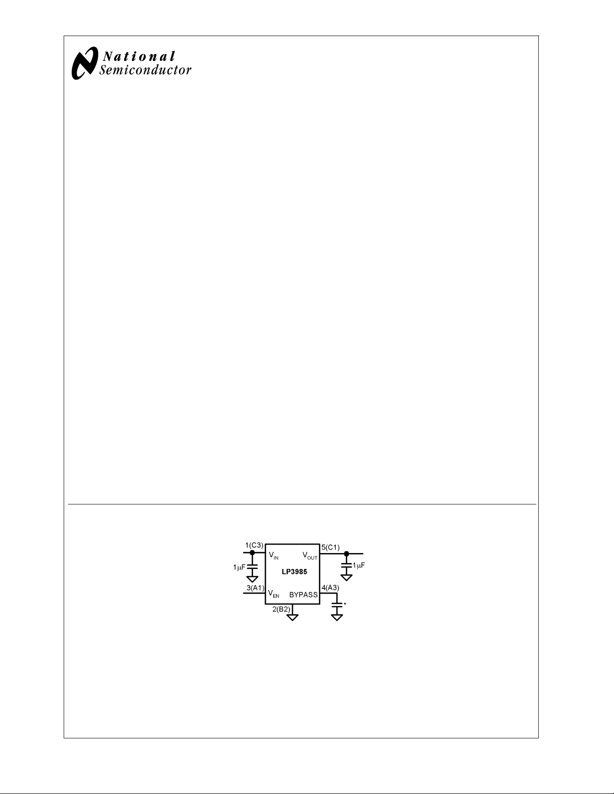
LP3985 Micropower, 150mA Low-Noise Ultra Low-Dropout CMOS Voltage Regulator
Typical Application Circuit
Note: Pin Numbers in parenthesis indicate micro SMD package.
*
Optional Noise Reduction Capacitor.
© 2003 National Semiconductor Corporation DS101364 www.national.com
10136402
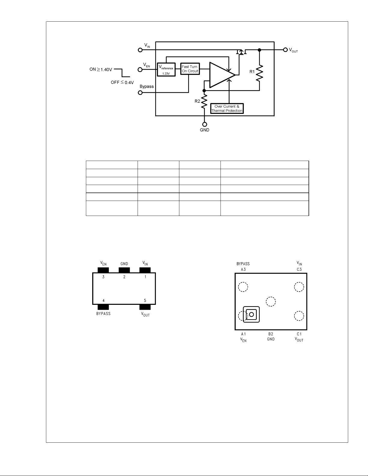
Block Diagram
LP3985
Pin Description
10136401
Name * micro SMD SOT Function
V
EN
A1 3 Enable Input Logic, Enable High
GND B2 2 Common Ground
V
OUT
V
IN
C1 5 Output Voltage of the LDO
C3 1 Input Voltage of the LDO
BYPASS A3 4 Optional Bypass Capacitor for Noise
Reduction
* The pin numbering scheme for the micro SMD package was revised in April 2002 to conform to JEDEC standard. Only the pin numbers were
revised. No changes to the physical location of the inputs/outputs were made. For reference purposes, the obsolete numbering scheme had VEN
as pin 1, GND as pin 2, VOUT as pin 3, VIN as pin 4, and BYPASS as pin 5.
Connection Diagrams
SOT 23-5 Package (MF) 5 Bump micro SMD Package (BPA05, BLA05, TLA05)
Top View
See NS Package Number MF05A
10136407
10136470
Top View
See NS Package Number BPA05, BLA05, TLA05
www.national.com 2
Ordering Information
BP refers to 0.170mm bump size, 0.900mm height for micro SMD Package
Output
Voltage (V)
2.5 STD LP3985IBP-2.5 LP3985IBPX-2.5
2.6 STD LP3985IBP-2.6 LP3985IBPX-2.6
2.7 STD LP3985IBP-2.7 LP3985IBPX-2.7
2.8 STD LP3985IBP-2.8 LP3985IBPX-2.8
2.85 STD LP3985IBP-285 LP3985IBPX-285
2.9 STD LP3985IBP-2.9 LP3985IBPX-2.9
3.0 STD LP3985IBP-3.0 LP3985IBPX-3.0
3.1 STD LP3985IBP-3.1 LP3985IBPX-3.1
3.2 STD LP3985IBP-3.2 LP3985IBPX-3.2
3.3 STD LP3985IBP-3.3 LP3985IBPX-3.3
4.7 STD LP3985IBP-4.7 LP3985IBPX-4.7
5.0 STD LP3985IBP-5.0 LP3985IBPX-5.0
BL refers to 0.300mm bump size, 0.995mm height for micro SMD Package
Output
Voltage (V)
2.5 STD LP3985IBL-2.5 LP3985IBLX-2.5
2.6 STD LP3985IBL-2.6 LP3985IBLX-2.6
2.7 STD LP3985IBL-2.7 LP3985IBLX-2.7
2.8 STD LP3985IBL-2.8 LP3985IBLX-2.8
2.85 STD LP3985IBL-285 LP3985IBLX-285
2.9 STD LP3985IBL-2.9 LP3985IBLX-2.9
3.0 STD LP3985IBL-3.0 LP3985IBLX-3.0
3.1 STD LP3985IBL-3.1 LP3985IBLX-3.1
3.2 STD LP3985IBL-3.2 LP3985IBLX-3.2
3.3 STD LP3985IBL-3.3 LP3985IBLX-3.3
4.8 STD LP3985IBL-4.8 LP3985IBLX-4.8
5.0 STD LP3985IBL-5.0 LP3985IBLX-5.0
Grade
Grade
LP3985 Supplied as 250
Units, Tape and Reel
LP3985 Supplied as 250
Units, Tape and Reel
LP3985
LP3985 Supplied as 3000
Units, Tape and Reel
LP3985 Supplied as 3000
Units, Tape and Reel
TL refers to 0.300mm bump size, 0.600mm height for micro SMD Package
Output
Voltage (V)
2.5 STD LP3985ITL-2.5 LP3985ITLX-2.5
2.6 STD LP3985ITL-2.6 LP3985ITLX-2.6
2.7 STD LP3985ITL-2.7 LP3985ITLX-2.7
2.8 STD LP3985ITL-2.8 LP3985ITLX-2.8
2.85 STD LP3985ITL-285 LP3985ITLX-285
2.9 STD LP3985ITL-2.9 LP3985ITLX-2.9
3.0 STD LP3985ITL-3.0 LP3985ITLX-3.0
3.1 STD LP3985ITL-3.1 LP3985ITLX-3.1
3.2 STD LP3985ITL-3.2 LP3985ITLX-3.2
3.3 STD LP3985ITL-3.3 LP3985ITLX-3.3
4.8 STD LP3985ITL-4.8 LP3985ITLX-4.8
5.0 STD LP3985ITL-5.0 LP3985ITLX-5.0
Grade
LP3985 Supplied as 250
Units, Tape and Reel
LP3985 Supplied as 3000
Units, Tape and Reel
www.national.com3
Ordering Information (Continued)
LP3985
Output
Voltage (V)
2.5 STD LP3985IM5-2.5 LP3985IM5X-2.5 LCSB
2.6 STD LP3985IM5-2.6 LP3985IM5X-2.6 LCTB
2.7 STD LP3985IM5-2.7 LP3985IM5X-2.7 LCUB
2.8 STD LP3985IM5-2.8 LP3985IM5X-2.8 LCJB
2.85 STD LP3985IM5-285 LP3985IM5X-285 LCXB
2.9 STD LP3985IM5-2.9 LP3985IM5X-2.9 LCYB
3.0 STD LP3985IM5-3.0 LP3985IM5X-3.0 LCRB
3.1 STD LP3985IM5-3.1 LP3985IM5X-3.1 LCZB
3.2 STD LP3985IM5-3.2 LP3985IM5X-3.2 LDPB
3.3 STD LP3985IM5-3.3 LP3985IM5X-3.3 LDQB
4.7 STD LP3985IM5-4.7 LP3985IM5X-4.7 LDRB
5.0 STD LP3985IM5-5.0 LP3985IM5X-5.0 LDSB
Grade
For SOT Package
LP3985 Supplied as 1000
Units, Tape and Reel
LP3985 Supplied as 3000
Units, Tape and Reel
Package Marking
www.national.com 4
LP3985
Absolute Maximum Ratings (Notes 1,
2)
If Military/Aerospace specified devices are required,
please contact the National Semiconductor Sales Office/
Distributors for availability and specifications.
V
IN,VEN
V
OUT
-0.3 to (VIN+0.3) ≤ 6.5V
Junction Temperature 150˚C
Storage Temperature −65˚C to +150˚C
Lead Temp. 235˚C
−0.3 to 6.5V
Operating Ratings (Notes 1, 2)
V
IN
V
EN
Junction Temperature −40˚C to +125˚C
Thermal Resistance
θ
(SOT23-5)
JA
(micro SMD)
θ
JA
Maximum Power Dissipation
SOT23-5 (Note 6)
micro SMD (Note 6)
Pad Temp. (Note 3) 235˚C
Maximum Power Dissipation
SOT23-5 (Note 4)
micro SMD (Note 4)
364mW
355mW
ESD Rating(Note 5)
Human Body Model
Machine Model
2kV
150V
Electrical Characteristics
Unless otherwise specified: VIN=V
OUT(nom)
and limits appearing in standard typeface are for T
temperature range for operation, −40˚C to +125˚C. (Note 7) (Note 8)
Symbol Parameter Conditions Typ
Output Voltage
Tolerance
Line Regulation Error VIN=(V
∆V
OUT
Load Regulation Error
(Note 9)
Output AC Line Regulation V
PSRR Power Supply Rejection Ratio
I
Q
Quiescent Current VEN= 1.4V, I
Dropout Voltage (Note 10) I
I
SC
I
OUT(PK)
Short Circuit Current Limit Output Grounded
Peak Output Current V
+ 0.5V, CIN= 1 µF, I
= 25˚C. Limits appearing in boldface type apply over the entire junction
J
I
= 1mA −2
OUT
OUT(nom)
= 1mA, C
OUT
+ 0.5V) to 6.0V,
OUT
= 1 µF, C
For 4.7 to 5.0 options
For all other options
= 1 mA to 150 mA
I
OUT
LP3985IM5 (SOT23-5)
LP3985 (micro SMD) 0.0004 0.002
IN=VOUT(nom)
= 150 mA (Figure 1)
I
OUT
V
IN=VOUT(nom)
+ 1V,
+ 0.2V,
f = 1 kHz,
=50mA(Figure 2)
I
OUT
V
IN=VOUT(nom)
+ 0.2V,
f = 10 kHz,
=50mA(Figure 2)
I
OUT
=0mA
OUT
For 4.7 to 5.0 options
For all other options
EN
= 1.4V, I
= 0 to 150 mA
OUT
For 4.7 to 5.0 options
For all other options
= 0.4V 0.003 1.5
V
EN
=1mA 0.4 2
OUT
I
=50mA 20 35
OUT
I
= 100 mA 45 70
OUT
I
= 150 mA 60 100
OUT
(Steady State)
OUT
≥ V
OUT(nom)
- 5% 550 300 mA
0to(VIN+0.3) ≤ 6V
= 0.01µF. Typical values
BYPASS
Limit
Min Max
2
−3
−0.19
−0.1
3
0.19
0.1
0.0025 0.005
1.5
50
40
100
85
155
140
165
150
250
200
600
2.5 to 6V
220˚C/W
255˚C/W
250mW
244mW
Units
%of
V
OUT(nom)
%/V
%/mA
mV
P-P
dB
µAV
mV
mA
www.national.com5
Electrical Characteristics (Continued)
LP3985
Unless otherwise specified: VIN=V
OUT(nom)
and limits appearing in standard typeface are for T
temperature range for operation, −40˚C to +125˚C. (Note 7) (Note 8)
Symbol Parameter Conditions Typ
T
ON
Turn-On Time
(Note 11)
e
n
Output Noise Voltage(Note 12) BW = 10 Hz to 100 kHz,
Output Noise Density C
+ 0.5V, CIN= 1 µF, I
= 25˚C. Limits appearing in boldface type apply over the entire junction
J
C
C
= 0.01 µF 200
BYPASS
= 1µF
OUT
= 0 230 nV/
BP
OUT
= 1mA, C
OUT
= 1 µF, C
= 0.01µF. Typical values
BYPASS
Limit
Min Max
30 µVrms
Units
µs
I
EN
V
IL
Maximum Input Current at EN VEN= 0.4 and VIN= 6.0
Maximum Low Level Input
VIN= 2.5 to 6.0V 0.4 V
±
1nA
Voltage at EN
V
IH
Minimum High Level Input
VIN= 2.5 to 6.0V 1.4 V
Voltage at EN
C
OUT
Output Capacitor Capacitance 120µF
ESR 5 500 mΩ
TSD
Note 1: Absolute Maximum Ratings are limits beyond which damage to the device may occur. Operating Ratings are conditions under which operation of the device
is guaranteed. Operating Ratings do not imply guaranteed performance limits. For guaranteed performance limits and associated test conditions, see the Electrical
Characteristics tables.
Note 2: All voltages are with respect to the potential at the GND pin.
Note 3: Additional information on lead temperature and pad temperature can be found in National Semiconductor Application Note (AN-1112).
Note 4: The Absolute Maximum power dissipation depends on the ambient temperature and can be calculated using the formula: P
where T
appearing under Absolute Maximum Ratings results from substituting the Absolute Maximum junction temperature, 150˚C, for T
More power can be dissipated safely at ambient temperatures below 70˚C . Less power can be dissipated safely at ambient temperatures above 70˚C. The Absolute
Maximum power dissipation can be increased by 4.5mW for each degree below 70˚C, and it must be derated by 4.5mW for each degree above 70˚C.
Note 5: The human body model is 100pF discharged through 1.5kΩ resistor into each pin. The machine model is a 200 pF capacitor discharged directly into each
pin.
Note 6: Like the Absolute Maximum power dissipation, the maximum power dissipation for operation depends on the ambient temperature. The 250mW rating for
SOT23-5 appearing under Operating Ratings results from substituting the maximum junction temperature for operation, 125˚C, for T
θ
JA
The maximum power dissipation for operation can be increased by 4.5mW for each degree below 70˚C, and it must be derated by 4.5mW for each degree above
70˚C.
Note 7: All limits are guaranteed. All electrical characteristics having room-temperature limits are tested during production with T
Statistical Quality Control (SQC) methods. All hot and cold limits are guaranteed by correlating the electrical characteristics to process and temperature variations
and applying statistical process control.
Note 8: The target output voltage, which is labeled V
Note 9: An increase in the load current results in a slight decrease in the output voltage and vice versa.
Note 10: Dropout voltage is the input-to-output voltage difference at which the output voltage is 100mV below its nominal value. This specification does not apply
for input voltages below 2.5V.
Note 11: Turn-on time is time measured between the enable input just exceeding V
Note 12: The output noise varies with output voltage option. The 30µVrms is measured with 2.5V voltage option. To calculate an approximated output noise for other
options, use the equation: (30µVrms)(X)/2.5, where X is the voltage option value.
Thermal Shutdown Temperature 160 ˚C
Thermal Shutdown Hysteresis 20 ˚C
=(TJ-TA)/θJA,
is the junction temperature, TAis the ambient temperature, and θJAis the junction-to-ambient thermal resistance. The 364mW rating for SOT23-5
J
into (Note 4) above. More power can be dissipated at ambient temperatures below 70˚C . Less power can be dissipated at ambient temperatures above 70˚C.
, is the desired voltage option.
OUT(nom)
and the output voltage just reaching 95% of its nominal value.
IH
D
, 70˚C for TA, and 220˚C/W for θJA.
J
, 70˚C for TA, and 220˚C/W for
J
= 25˚C or correlated using
J
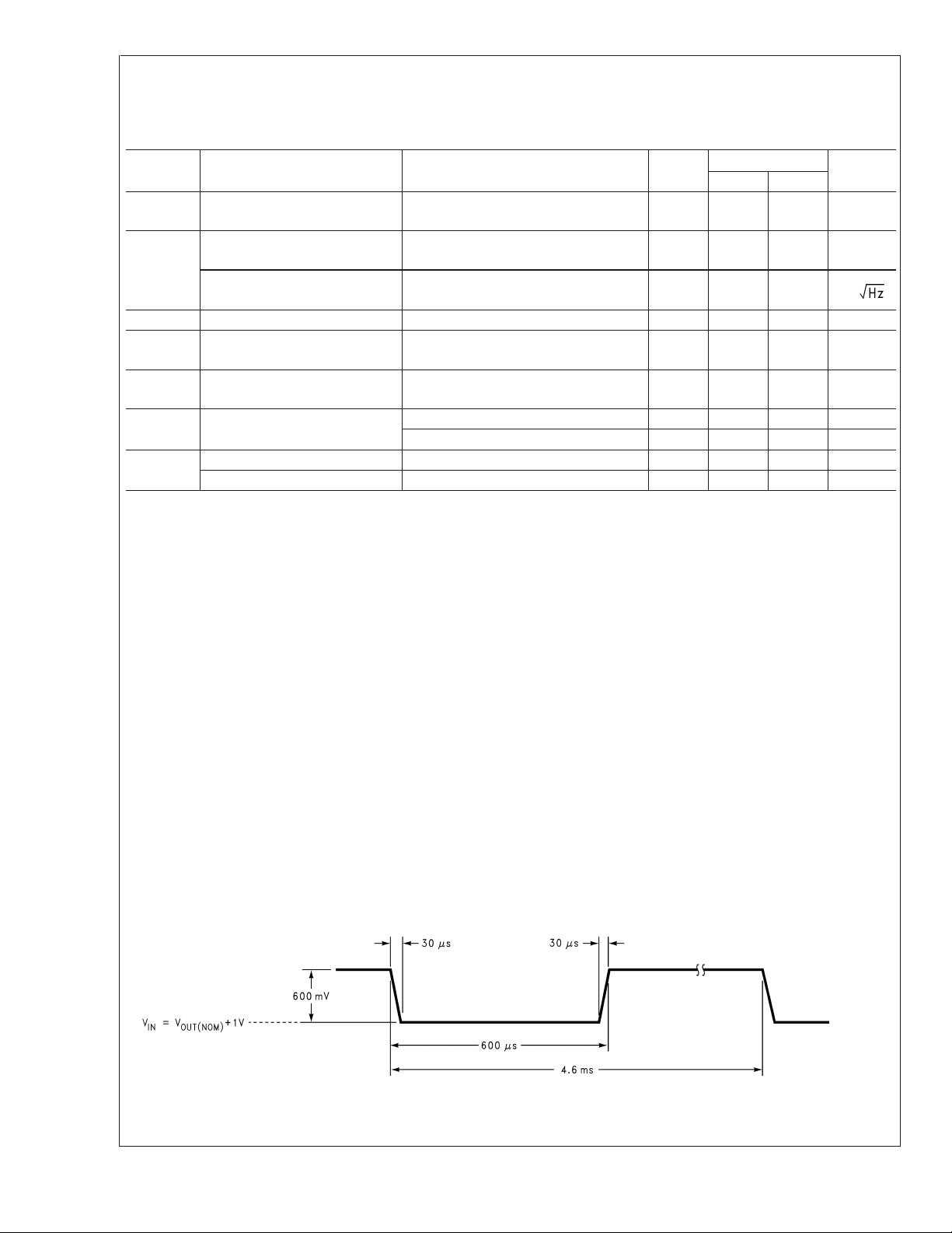
10136408
FIGURE 1. Line Transient Input Test Signal
www.national.com 6
 Loading...