

LP3983
Micropower, Low Quiescent Current, CMOS Voltage
Regulator in micro SMD Package
LP3983 Micropower, Low Quiescent Current, CMOS Voltage Regulator in micro SMD Package
May 2003
General Description
The LP3983 is a fixed voltage low current regulator.
The LP3983 is ideally suited to standby type applications in
battery powered equipment, it allows the lifetime of the battery to be maximized. The device can be controlled via an
Enable(disable) control and can thus be used by the system
to further extend the battery lifetime by reducing the power
consumption to virtually zero.
Performance is specified for a -40˚C to 125˚C temperature
range.
For output voltages other than those stated and alternative
package options, please contact your local NSC sales office.
Features
n Miniature 5 pin package
n Logic Controlled Enable
n No Noise Bypass Capacitor Required
n Stable with Low ESR Ceramic Capacitors
n Fast turn ON
n Short Circuit Protection
Package
n Tiny 5 Pin micro SMD 828µm by 1387µm
Key Specifications
n Input Voltage Range 2.5 to 6.0V
n Output Voltages 1.6, 1.8, & 2.5
n Output Current 5mA
n Output Capacitors 1µF Low ESR
n Virtually Zero I
n Low I
n PSRR 10dB
n Fast Start Up 170µs
(Enabled) 14µA
Q
(Disabled) 1.0µA
Q
Applications
n GSM Portable Phones
n CDMA Cellular Handsets
n Bluetooth Devices
n Portable Information Appliances
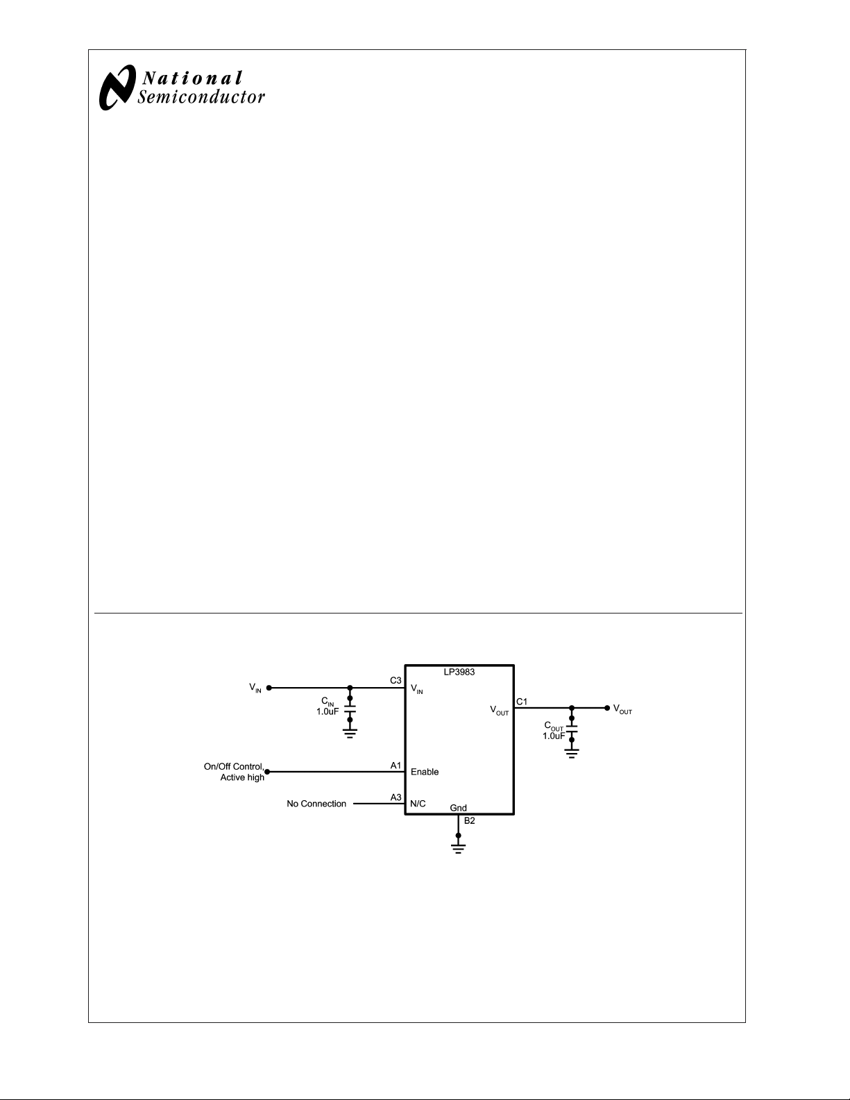
Typical Application Circuit
20057601
© 2003 National Semiconductor Corporation DS200576 www.national.com
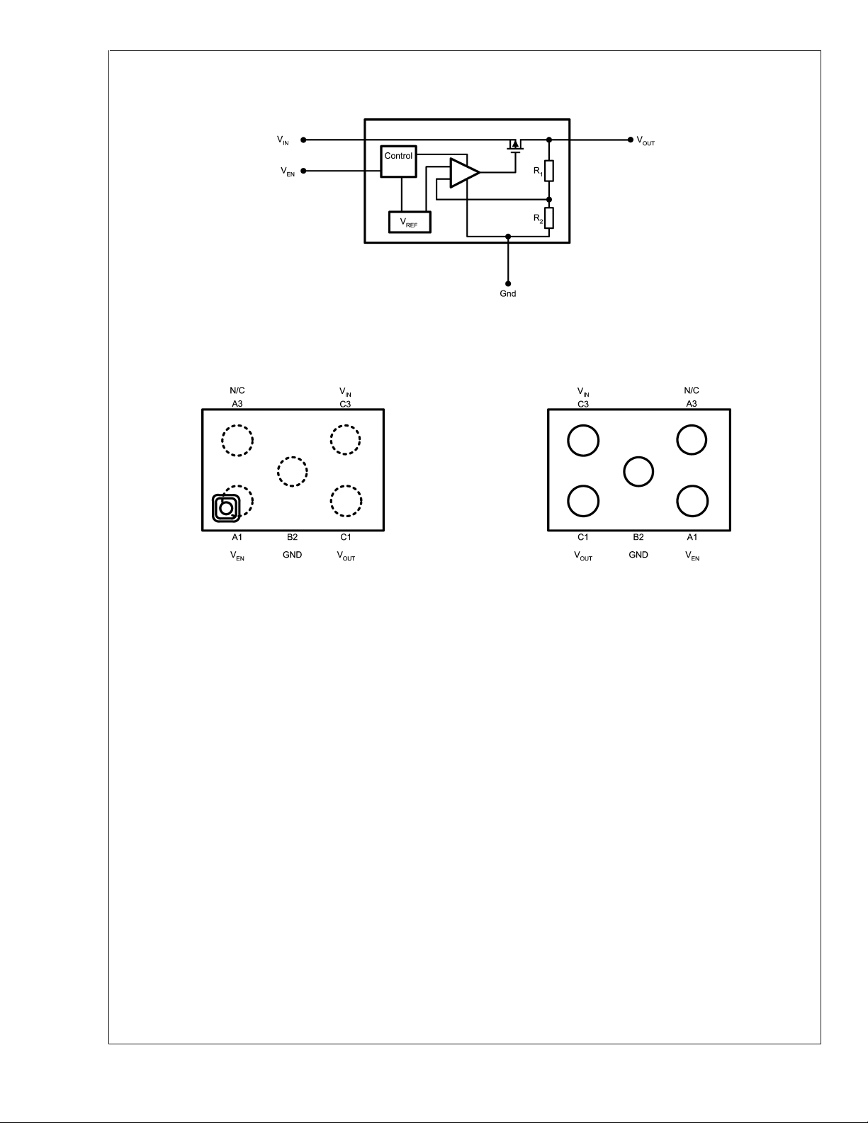
Block Diagram
LP3983
Connection Diagrams
5 Pin micro SMD Package 5 Pin micro SMD Package
LP3983
20057602
Top View
20057603
See NS Package Number TLA05
Bottom View
20057604
See NS Package Number TLA05
www.national.com 2
Pin Descriptions
Name Pin No. Name and Function
V
EN
A1 Enable Input Logic,
Enables regulator when ≥ 1.2V. Disables regulator when ≤ 0.5V
GND B2 Common Ground
V
OUT
V
IN
C1 Voltage Output. Connect this Output to the Load Circuit.
C3 Unregulated supply Input.
N/C A3 No Connection. There should be no electrical connection made to
this pin.
Ordering Information
TL refers as 0.300mm bump size with package height of 0.6mm
Output
Voltage (V)
Grade
1.6 STD LP3983ITL-1.6 LP3983ITLX-1.6
1.8 STD LP3983ITL-1.8 LP3983ITLX-1.8
2.5 STD LP3983ITL-2.5 LP3983ITLX-2.5
* Please contact National Semiconductor for availability
LP3983 Supplied as 250
Units, Tape and Reel
LP3983
LP3983 Supplied as 3000
Units, Tape and Reel
www.national.com3

Absolute Maximum Ratings (Notes 1,
2)
LP3983
Machine Model 100V
If Military/Aerospace specified devices are required,
please contact the National Semiconductor Sales Office/
Distributors for availability and specifications.
V
IN
V
EN
−0.3 to (VIN+ 0.3V) to
−0.3 to 6.5V
6.5V(max)
V
OUT
−0.3V to(VIN+ 0.3V) to
6.5V(max)
Junction Temperature 150˚C
Operating Ratings (Notes 1, 2)
V
(Note 9) V
IN
V
, 0 to 6.0V
EN
Recommended Load Current 0 to 5mA
Junction Temperature −40˚C to +125˚C
Ambient Temperature
(Note 3)
−40˚C to +119˚C
Storage Temperature −65˚C to +150˚C
Pad Temperature
(Soldering, 10 sec.)
ESD (Note 4)
265˚C
Thermal Properties (Note 3)
Junction to Ambient Thermal
Resistance (θ
)
JA
Human Body Model 2KV
Electrical Characteristics
Unless otherwise specified: VEN= 1.8V,VIN=V
OUT(nom)
and limits appearing in standard typeface are for T
temperature range for operation, −40˚C to +125˚C. (Note 10) (Note 11)
Symbol Parameter Conditions Typ
Output Voltage
∆V
OUT
Tolerance
PSRR Power Supply Rejection
Ratio
I
Q
I
SC
Quiescent Current I
Short Circuit Current
I
= 0mA to 5mA -55 +55
OUT
VIN=V
f ≤10 kHz, I
= 50µA, VIN= 4.2V 14 21
OUT
V
= 0.4V, VIN= 4.2V 1 3
EN
Output Grounded
Limit (Note 7)
I
OUT
Maximum Output
Current (Note 6)
Logic Control Characteristics
I
EN
V
IL
Maximum Input Current
input
at V
EN
Logic Low Input
V
= 0.4 and VIN= 6.0V
EN
VIN=V
Threshold
V
IH
Logic High Input
VIN=V
Threshold
Timing Characteristics
T
ON
Note 1: Absolute Maximum Ratings are limits beyond which damage to the device may occur. Operating Ratings are conditions under which operation of the device
is guaranteed. Operating Ratings do not imply guaranteed performance limits. For guaranteed performance limits and associated test conditions, see the Electrical
Characteristics tables.
Note 2: All voltages are with respect to the potential at the GND pin.
Note 3: The maximum ambient temperature (T
dissipation of the device in te application (P
following equation: T
Note 4: The human body model is 100pF discharged through a 1.5kΩ resistor into each pin. The machine model is a 200pF capacitor discharged directly into each
pin.
Note 5: Junction to ambient thermal resistance is dependant on the application and board layout. In applications where high maximum power dissipation is possible,
special care must be paid to thermal dissipation issues in board design.
Note 6: The device maintains the regulated output voltage without load.
Turn on Time(Note 7) (Note 8) 170 250 µs
) is dependant on the maximum operating junction temperature (T
A(max)
), and the junction to ambient thermal resistance of the part/package in the application (θJA), as given by the
D(max)
A(max)=TJ(max-op)
-(θJAxP
D(max)
).
+ 1.0V, CIN= 1.0 µF, I
= 25˚C. Limits appearing in boldface type apply over the entire junction
J
= 1.0mA, C
OUT
= 1.0 µF. Typical values
OUT
Limit
Min Max
-96 +96
−6 +6
OUT
+ 1V,
= 1mA
10 dB
OUT(nom)
28 35 mA
5 mA
0.02 µA
to 6.0V
IN(MIN)
IN(MIN)
to 6.0V
1.2 V
J(max-op)
0.5 V
= 125˚C), the maximum power
IN(MIN)
255˚C/W
mV from
V
OUT(nom)
%of
V
OUT(nom)
to 6V
Units
µA
www.national.com 4

Electrical Characteristics (Continued)
Note 7: This electrical specification is guaranteed by design.
Note 8: Time from V
Note 9: The minimum VINis dependant on the device output option.
For V
OUT(NOM)
Note 10: All limits are guaranteed. All electrical characteristics having room-temperature limits are tested during production with T
Statistical Quality Control methods. Operation over the temperature specification is guaranteed by correlating the electrical characteristics to process and
temperature variations and applying statistical process control.
Note 11: The target output voltage which is labelled V
EN
≤ 2.7V, V
= 1.2V to V
IN(MIN)
= 95% of V
OUT
will equal 2.5V. For V
OUT(NOM)
OUT(NOM)
OUT(NOM)
>
2.7V, V
is the desired voltage option.
IN(MIN)
will equal V
OUT(NOM)
+ 200mV.
= 25˚C or correlated using
J
Output Capacitor, Recommended Specifications
Symbol Parameter Conditions Value
C
o
Output Capacitor Capacitance(Note 12) 1.0 0.75 µF
ESR 5 500 mΩ
Note 12: The capacitor tolerance should be±25% or better over the temperature range. Capacitor types recommended are X7R, Y5V, and Z5U.
Limit
Min Max
LP3983
Units
www.national.com5

Typical Performance Characteristics Unless otherwise specified, C
=V
LP3983
OUT(nom)
+ 1.0V, TA= 25˚C, Enable pin is tied to VIN.
@
Ground Current
Ripple Rejection (CIN=C
TA= 25˚C Ground Current vs VIN.I
= 1µF, IL= 100µA) Start Up Time. V
OUT
20057626 20057628
IN=COUT
OUT
= 1 µF Ceramic, V
= 7mA
OUT
= 1.8V
IN
Turn-Off Time. V
20057627
= 1.8V Load Transient Response. V
OUT
20057615
OUt
20057608
= 1.8V
20057616
www.national.com 6

LP3983
Typical Performance Characteristics Unless otherwise specified, C
V
+ 1.0V, TA= 25˚C, Enable pin is tied to VIN. (Continued)
OUT(nom)
Line Transient Response
20057636
IN=COUT
= 1 µF Ceramic, VIN=
www.national.com7

Application Hints
LP3983
POWER DISSIPATION AND DEVICE OPERATION
The permissible power dissipation for any package is a
measure of the capability of the device to pass heat from the
power source, the junctions of the IC, to the ultimate heat
sink, the ambient environment. Thus the power dissipation is
dependent on the ambient temperature and the thermal
resistance across the various interfaces between the die and
ambient air.
As stated in note 3 in the electrical specification section, the
allowable power dissipation for the device in a given package can be calculated using the equation
=(TJ-TA)/θ
P
D
With a θJA= 255˚C/W, the device in the micro SMD package
returns a value of 392mW with a maximum junction temperature of 125˚C and an ambient temperature of 25˚C. The
actual power dissipation across the device can be represented by the following equation;
=(VIN-V
P
D
This establishes the relationship between the power dissipation allowed due to thermal considerations, the voltage drop
across the device, and the continuous current capability of
the device. These two equations should be used to determine the optimum operating conditions for the device in the
application.
EXTERNAL CAPACITORS
In common with most low-dropout regulators, the LP3983
requires external capacitors to ensure stable operation. The
LP3983 is specifically designed for portable applications
requiring minimum board space and smallest components.
These capacitors must be correctly selected for good performance.
INPUT CAPACITOR
An input capacitor is required for stability. It is recommended
that a 1.0uF capacitor be connected between the LP3983
input pin and ground (this capacitance value may be increased without limit).
This capacitor must be located a distance of not more than
1cm from the input pin and returned to a clean analog
ground. Any good quality ceramic, tantalum, or film capacitor
may be used at the input.
Important: Tantalum capacitors can suffer catastrophic failures due to surge current when connected to a lowimpedance source of power (like a battery or a very large
capacitor). If a tantalum capacitor is used at the input, it must
be guaranteed by the manufacturer to have a surge current
rating sufficient for the application.
There are no requirements for the ESR (Equivalent Series
Resistance) on the input capacitor, but tolerance and temperature coefficient must be considered when selecting the
capacitor to ensure the capacitance will be ) 1µF over the
entire operating temperature range.
OUTPUT CAPACITOR
The LP3983 is designed specifically to work with very small
ceramic output capacitors. A ceramic capacitor (dielectric
types Z5U, Y5V or X7R), recommended value 2.2µF and
with ESR between 5mΩ to 500mΩ, is suitable in the LP3983
application circuit.
For this device the output capacitor should be connected
between the VOUT pin and ground.
OUT
JA
)*I
OUT
It may also be possible to use tantalum or film capacitors at
the output, but these are not as attractive for reasons of size
and cost (see the section Capacitor Characteristics).
NO-LOAD STABILITY
The LP3983 will remain stable and in regulation with no
external load. This is specially important in CMOS RAM
keep-alive applications.
CAPACITOR CHARACTERISTICS
The LP3983 is designed to work with ceramic capacitors on
the output to take advantage of the benefits they offer. For
capacitance values in the range of 1µF to 4.7µF range,
ceramic capacitors are the smallest, least expensive and
have the lowest ESR values (which makes them best for
eliminating high frequency noise). The ESR of a typical 1µF
ceramic capacitor is in the range of 20 mΩ to 40 mΩ, which
easily meets the ESR requirement for stability by the
LP3983.
The temperature performance of ceramic capacitors varies
by type. Larger value ceramic capacitors may be manufactured with Z5U or Y5V temperature characteristics, which
results in the capacitance dropping by more than 50% as the
temperature goes from 25˚C to 85˚C.
A better choice for temperature coefficient in a ceramic
±
capacitor is X7R, which holds the capacitance within
15%
over the temperature range. Tantalum capacitors are less
desirable than ceramic for use as output capacitors because
they are more expensive when comparing equivalent capacitance and voltage ratings in the 1µF to 4.7µF range.
Another important consideration is that tantalum capacitors
have higher ESR values than equivalent size ceramics. This
means that while it may be possible to find a tantalum
capacitor with an ESR value within the stable range, it would
have to be larger in capacitance (which means bigger and
more costly ) than a ceramic capacitor with the same ESR
value. It should also be noted that the ESR of a typical
tantalum will increase about 2:1 as the temperature goes
from 25˚C down to −40˚C, so some guard band must be
allowed.
ENABLE OPERATION
The LP3983 may be switched ON or OFF by a logic input at
the ENABLE pin, V
. A high voltage at this pin will turn the
EN
device on. When the enable pin is low, the regulator output is
<
off and the device typically consumes
tion does not require the shutdown feature, the V
should be tied to V
to keep the regulator output perma-
IN
1µA. If the applica-
pin
EN
nently on. To ensure proper operation, the signal source
used to drive the V
input must be able to swing above and
EN
below the specified turn-on/off voltage thresholds listed in
the Electrical Characteristics section under V
and VIH.
IL
MICRO SMD MOUNTING
The micro SMD package requires specific mounting techniques which are detailed in National Semiconductor Application Note (AN-1112).
Referring to the section Surface Mount Technology (SMT)
Assembly Considerations, it should be noted that the pad
style which must be used with the 5 pin package is NSMD
(non-solder mask defined) type.
For best results during assembly, alignment ordinals on the
PC board may be used to facilitate placement of the micro
SMD device.
www.national.com 8

Application Hints (Continued)
MICRO SMD LIGHT SENSITIVITY
Exposing the micro SMD device to direct sunlight may cause
mis-operation of the device. Light sources such as Halogen
lamps can effect electrical performance if brought near to the
device.
Light with wavelengths in the red and infra-red part of the
spectrum have the most detrimental effect thus the fluores-
LP3983
cent lighting used inside most buildings has very little effect
on the output voltage of the device. Tests carried out on a
micro SMD test board showed a negligible effect on the
regulated output voltage when brought within 1cm of a fluorescent lamp. A deviation of less than 0.1% from nominal
output voltage was observed.
www.national.com9

Physical Dimensions inches (millimeters) unless otherwise noted
micro SMD, 5 Bump, Package (TLA05)
NS Package Number TLA05ADA
The dimensions for X1, X2 and X3 are given as:
X1 = 1006 +/− 0.03mm
X2 = 1438 +/− 0.03mm
X3 = 0.600 +/− 0.075mm
LIFE SUPPORT POLICY
NATIONAL’S PRODUCTS ARE NOT AUTHORIZED FOR USE AS CRITICAL COMPONENTS IN LIFE SUPPORT
DEVICES OR SYSTEMS WITHOUT THE EXPRESS WRITTEN APPROVAL OF THE PRESIDENT AND GENERAL
COUNSEL OF NATIONAL SEMICONDUCTOR CORPORATION. As used herein:
1. Life support devices or systems are devices or
systems which, (a) are intended for surgical implant
into the body, or (b) support or sustain life, and
whose failure to perform when properly used in
accordance with instructions for use provided in the
2. A critical component is any component of a life
support device or system whose failure to perform
can be reasonably expected to cause the failure of
the life support device or system, or to affect its
safety or effectiveness.
labeling, can be reasonably expected to result in a
significant injury to the user.
National Semiconductor
Americas Customer
Support Center
LP3983 Micropower, Low Quiescent Current, CMOS Voltage Regulator in micro SMD Package
National does not assume any responsibility for use of any circuitry described, no circuit patent licenses are implied and National reserves the right at any time without notice to change said circuitry and specifications.
Email: new.feedback@nsc.com
Tel: 1-800-272-9959
www.national.com
National Semiconductor
Europe Customer Support Center
Fax: +49 (0) 180-530 85 86
Email: europe.support@nsc.com
Deutsch Tel: +49 (0) 69 9508 6208
English Tel: +44 (0) 870 24 0 2171
Français Tel: +33 (0) 1 41 91 8790
National Semiconductor
Asia Pacific Customer
Support Center
Email: ap.support@nsc.com
National Semiconductor
Japan Customer Support Center
Fax: 81-3-5639-7507
Email: jpn.feedback@nsc.com
Tel: 81-3-5639-7560
 Loading...