

April 2005
LP3981
Micropower, 300mA Ultra Low-Dropout CMOS Voltage
Regulator
General Description
The LP3981’s performance is optimized for battery powered
systems to deliver ultra low noise, extremely low dropout
voltage and low quiescent current. Regulator ground current
increases only slightly in dropout, further prolonging the
battery life.
Power supply rejection is better than 60 dB at low frequencies. This high power supply rejection is maintained down to
lower input voltage levels common to battery operated circuits.
The device is ideal for mobile phone and similar battery
powered wireless applications. It provides up to 300 mA,
from a 2.5V to 6V input, consuming less than 1µA in disable
mode.
The LP3981 is available in MSOP-8 package. For LP3981 in
LLP-6 package, contact NSC sales offices. Performance is
specified for −40˚C to +125˚C temperature range. The device available in the following output voltages; 2.5V, 2.7V,
2.8V, 2.83V, 3.0V, 3.03V and 3.3V as standard. Other output
options can be made available, please contact your local
NSC sales office.
Key Specifications
n 2.5 to 6.0V input range
n 300mA guaranteed output
n 60dB PSRR at 1kHz
n ≤1µA quiescent current when shut down
n Fast Turn-On time: 120 µs (typ.) with C
n 132mV typ dropout with 300mA load
n 35µVrms output noise over 10Hz to 100kHz
n −40 to +125˚C junction temperature range for operation
n 2.5V, 2.7V, 2.8V, 2.83V, 3.0V, 3.03V, and 3.3V outputs
standard
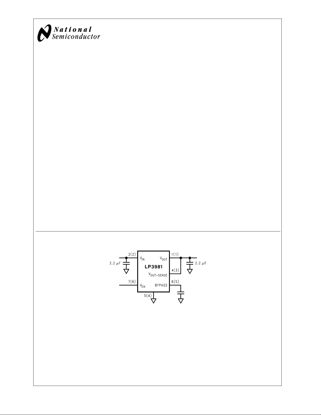
BYPASS
= 0.01uF
Features
n Small, space saving MSOP-8
n Low Thermal Resistance in LLP-6 package gives
excellent power capability
n Logic controlled enable
n Stable with ceramic and high quality tantalum capacitors
n Fast turn-on
n Thermal shutdown and short-circuit current limit
Applications
n CDMA cellular handsets
n Wideband CDMA cellular handsets
n GSM cellular handsets
n Portable information appliances
n Tiny 3.3V
±
5% to 2.5V, 300mA converter
LP3981 Micropower, 300mA Ultra Low-Dropout CMOS Voltage Regulator
Typical Application Circuit
Note: Pin Numbers in parenthesis indicate LLP-6 package.
© 2005 National Semiconductor Corporation DS200203 www.national.com
20020302
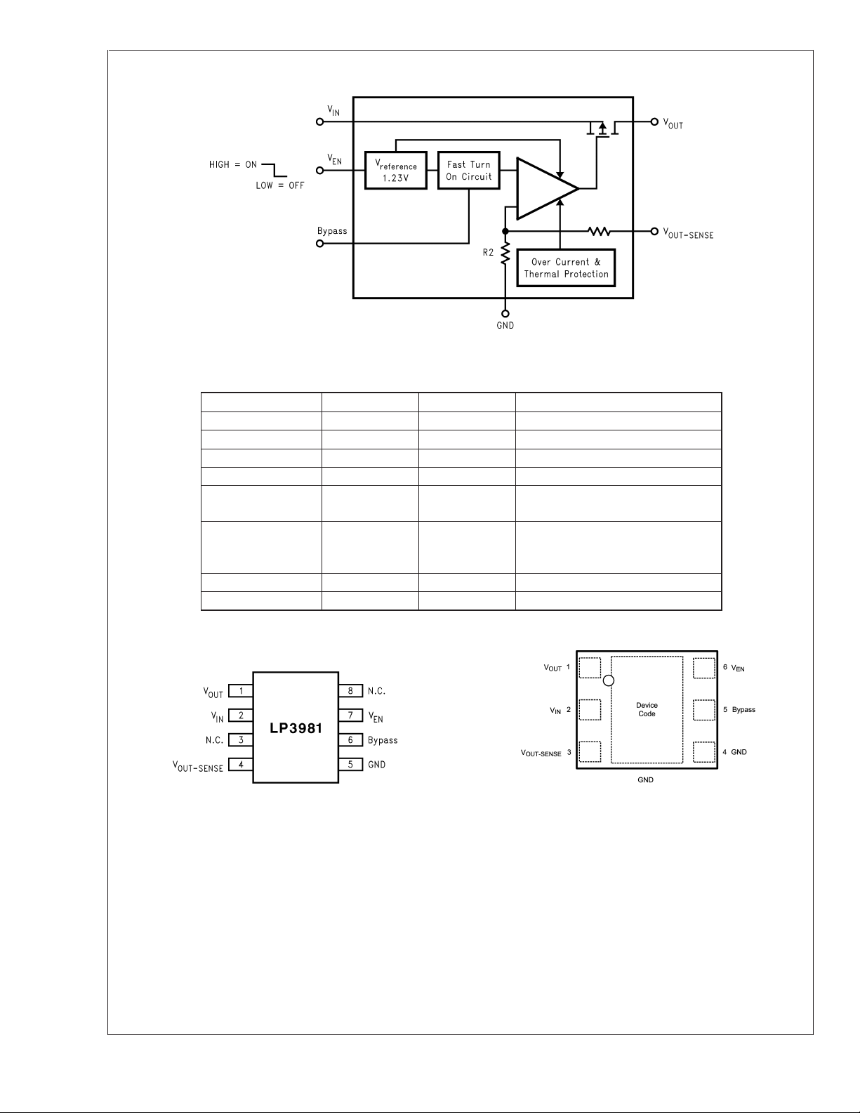
Block Diagram
LP3981
Pin Descriptions
Name MSOP-8 LLP-6 Function
V
EN
7 6 Enable Input Logic, Enable High.
GND 5 4 Common Ground. Connect to PAD.
V
OUT
V
IN
1 1 Output Voltage of the LDO.
2 2 Input Voltage of the LDO.
Bypass 6 5 Optional bypass capacitor for noise
reduction.
V
OUT-SENSE
4 3 Output. Voltage Sense Pin. Should
be connected to V
OUT
for proper
operation.
N.C 3, 8
GND PAD Common Ground. Connect to pin 4.
20020301
Connection Diagrams
MSOP-8 Package
Top View
See NS Package Number MUA008AE
20020307
LLP-6 Package
20020370
Top View
See NS Package Number LDC06D
www.national.com 2
Ordering Information
For LLP-6 Package
Output
Voltage (V)
2.5 STD LP3981ILD-2.5 LP3981ILDX-2.5 LO1UB
2.7 STD LP3981ILD-2.7 LP3981ILDX-2.7 LO1VB
2.8 STD LP3981ILD-2.8 LP3981ILDX-2.8 LO1ZB
2.83 STD LP3981ILD-2.83 LP3981ILDX-2.83 L01SB
3.0 STD LP3981ILD-3.0 LP3981ILDX-3.0 L017B
3.03 STD LP3981ILD-3.03 LP3981ILDX-3.03 LO1YB
3.3 STD LP3981ILD -3.3 LP3981ILDX-3.3 LO1XB
Output
Voltage (V)
2.5 STD LP3981IMM-2.5 LP3981IMMX-2.5 LFKB
2.7 STD LP3981IMM-2.7 LP3981IMMX-2.7 LFLB
2.8 STD LP3981IMM-2.8 LP3981IMMX-2.8 LFTB
2.83 STD LP3981IMM-2.83 LP3981IMMX-2.83 LDUB
3.0 STD LP3981IMM-3.0 LP3981IMMX-3.0 LF3B
3.03 STD LP3981IMM-3.03 LP3981IMMX-3.03 LFPB
3.3 STD LP3981IMM-3.3 LP3981IMMX-3.3 LFNB
*
Please contact factory regarding the availability of voltage options not listed here.
Grade
Grade
LP3981 Supplied as 1000
Units, Tape and Reel
For MSOP-8 Package
LP3981 Supplied as 1000
Units, Tape and Reel
LP3981 Supplied as 4500
Units, Tape and Reel
LP3981 Supplied as 3500
Units, Tape and Reel
Package Marking
LP3981
Package Marking
www.national.com3

Absolute Maximum Ratings (Notes 1, 2)
If Military/Aerospace specified devices are required,
LP3981
please contact the National Semiconductor Sales Office/
ESD Rating(Note 4)
Human Body Model
Machine Model
Distributors for availability and specifications.
V
IN,VEN
V
OUT,VOUT-SENSE
Junction Temperature 150˚C
Storage Temperature −65˚C to +150˚C
Lead Temp.
Pad Temp.
Power Dissipation (Note 3)
θ
(MSOP-8)
JA
(LLP-6)
θ
JA
−0.3 to 6.5V
−0.3 to VIN+ 0.3,
Max 6.5V
210˚C/W
50˚C/W
Operating Ratings (Notes 1, 2)
V
IN
V
EN
Junction Temperature −40˚C to +125˚C
Maximum Power Dissipation (Note 5)
MSOP-8
LLP-6
Maximum Power Dissipation at 25˚C
MSOP-8
LLP-6
595mW
2.5W
Electrical Characteristics
Unless otherwise specified: VEN= 1.2V, VIN=V
cal values and imits appearing in standard typeface are for T
junction temperature range for operation, −40˚C to +125˚C. (Notes 6, 7)
Symbol Parameter Conditions Typ
Output Voltage
Tolerance
∆V
OUT
Line Regulation Error
Load Regulation Error
(Note 8)
PSRR
I
Q
Power Supply Rejection Ratio
(Note 10)
Quiescent Current VEN= 1.2V, I
Dropout Voltage (Note 9)
I
SC
e
n
TSD
I
OUT(PK)
I
EN
V
IL
Short Circuit Current Limit Output Grounded
Output Noise Voltage BW = 10 Hz to 100 kHz,
Thermal Shutdown Temperature 160 ˚C
Thermal Shutdown Hysteresis 20 ˚C
Peak Output Current V
Maximum Input Current at V
EN
Logic Low Input threshold VIN= 2.7 to 6.0V 0.4 V
+ 0.5V, CIN= 2.2 µF, CBP= 0.033 µF, I
OUT
V
IN=VOUT
= 25˚C. Limits appearing in boldface type apply over the entire
J
+ 0.5V to 6.0V, T
<
A
+85˚C
V
IN=VOUT
I
OUT
V
IN=VOUT(nom)
+ 0.5V to 6.0V, TJ≤125˚C −0.2 0.2 %/V
= 1 mA to 300 mA 0.0003 0.005 %/mA
+ 1V,
f = 1 kHz,
=50mA(Figure 2)
I
OUT
V
IN=VOUT(nom)
+ 1V,
f = 10 kHz,
=50mA(Figure 2)
I
OUT
= 1 mA 70 120
OUT
V
= 1.2V, I
EN
= 2.5V(Note 12)
V
OUT
V
= 0.4V 0.003 1.5
EN
=1mA 0.5 5
I
OUT
= 200 mA 88 133
OUT
I
= 300 mA 132 200
OUT
= 1 to 300 mA,
OUT
(Steady State)
= 0.033µF
C
BP
≥ V
OUT
VEN= 0 and V
(nom) - 5% 455 300
OUT
IN
2kV
200V
2.7 to 6V
0toV
476mW
2.0W
= 1mA, C
OUT
Min Max
−2
−3
0.005 −0.1 0.1
OUT
Limit
= 2.2 µF. Typi-
Units
2
3
%of
V
OUT(nom)
%/V
50
55
170 210
dB
µA
mVI
600
mA
35 µVrms
0.001 µA
IN
www.national.com 4
 Loading...