

Page 1
查询LP3961供应商
LP3961/LP3964
800mA Fast Ultra Low Dropout Linear Regulators
LP3961/LP3964 800mA Fast Ultra Low Dropout Linear Regulators
May 2000
General Description
The LP3961/LP3964 series of fast ultra low-dropout linear
regulators operate from a +2.5V to +7.0V input supply.Wide
range of preset output voltage options are available. These
ultra low dropout linear regulators respond very fast to step
changes in load which makes them suitable for low voltage
microprocessor applications. The LP3961/LP3964 are developed on a CMOS process which allows low quiescent
current operation independent of output load current. This
CMOS process also allows the LP3961/LP3964 to operate
under extremely low dropout conditions.
Dropout Voltage: Ultra low dropout voltage; typically 24mV
at 80mA load current and 240mV at 800mA load current.
Ground Pin Current: Typically 4mA at 800mA load current.
Shutdown Mode: Typically 15µA quiescent current when
the shutdown pin is pulled low.
Error Flag: Error flag goes low when the output voltage
drops 10% below nominal value (for LP3961).
SENSE: Sense pin improves regulation at remote loads.
(For LP3964)
Precision Output Voltage: Multiple output voltage options
are available ranging from 1.2V to 5.0V and adjustable, with
a guaranteed accuracy of
±
3.0% over all conditions ( varying line, load, and tempera-
ture).
±
1.5% at room temperature, and
Features
n Ultra low dropout voltage
n Low ground pin current
n Load regulation of 0.02%
n 15µA quiescent current in shutdown mode
n Guaranteed output current of 0.8A DC
n Available in SOT-223,TO-263 and TO-220 packages
n Output voltage accuracy
n Error flag indicates output status (LP3961)
n Sense option improves better load regulation (LP3964)
n Extremely low output capacitor requirements
n Overtemperature/overcurrent protection
n −40˚C to +125˚C junction temperature range
±
1.5%
Applications
n Microprocessor power supplies
n GTL, GTL+, BTL, and SSTL bus terminators
n Power supplies for DSPs
n SCSI terminator
n Post regulators
n High efficiency linear regulators
n Battery chargers
n Other battery powered applications
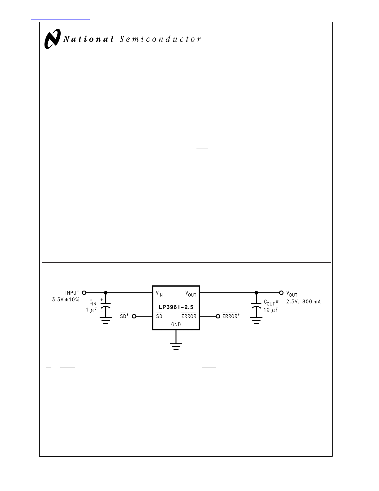
Typical Application Circuits
DS101129-1
#
Minimum output capacitance is 10 µF to ensure stability over full load current range. More capacitance provides superior dynamic performance and additional
stability margin.
*SD and ERROR pins must be pulled high through a 10kΩ pull-up resistor. Connect the ERROR pin to ground if this function is not used. See applications section for more information.
© 2000 National Semiconductor Corporation DS101129 www.national.com
Page 2
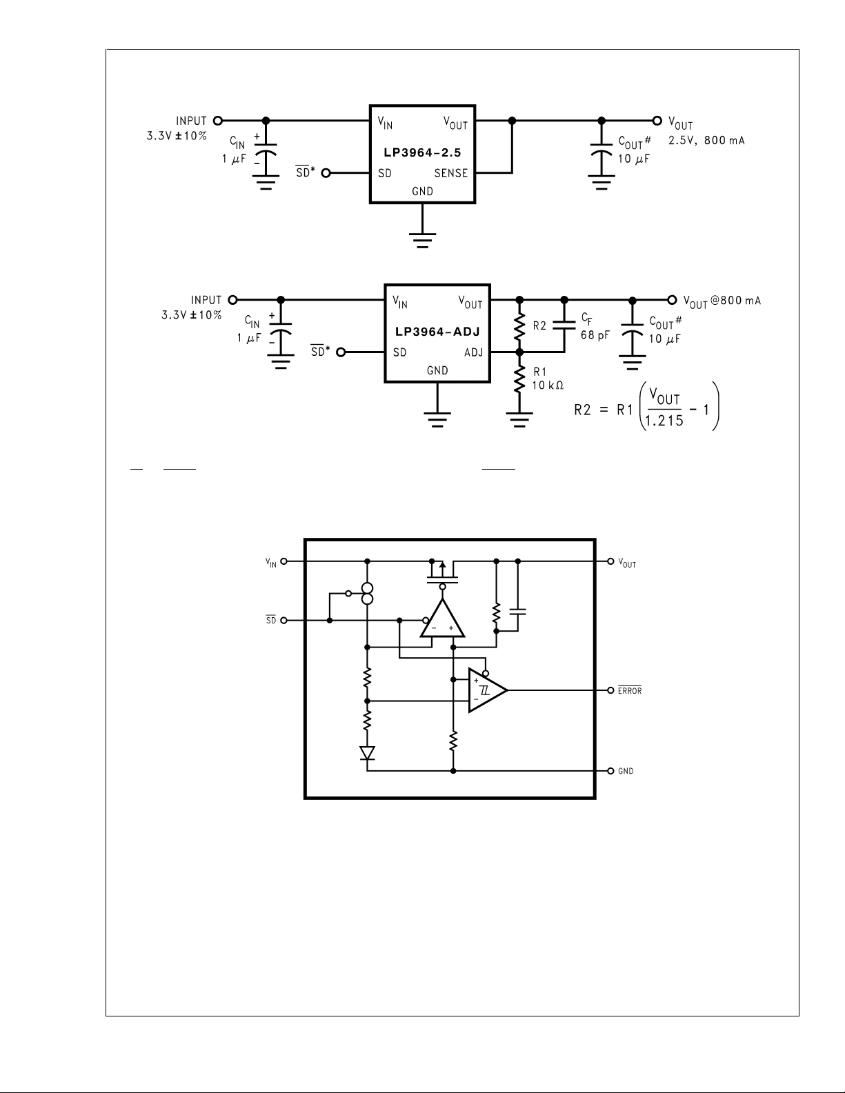
Typical Application Circuits (Continued)
LP3961/LP3964
#
Minimum output capacitance is 10 µF to ensure stability over full load current range. More capacitance provides superior dynamic performance and additional stability margin.
*SD and ERROR pins must be pulled high through a 10kΩ pull-up resistor. Connect the ERROR pin to ground if this function is not used. See applications section
for more information.
DS101129-2
Block Diagram LP3961
DS101129-3
www.national.com 2
Page 3
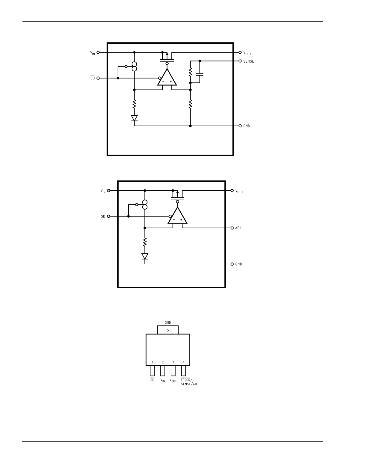
Block Diagram LP3964
Block Diagram LP3964-ADJ
LP3961/LP3964
DS101129-29
Connection Diagrams
DS101129-30
DS101129-4
Top View
SOT 223-5 Package
www.national.com3
Page 4
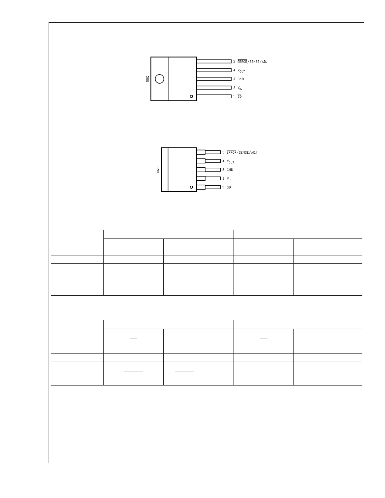
Connection Diagrams (Continued)
LP3961/LP3964
DS101129-5
Top View
TO220-5 Package
Bent, Staggered Leads
DS101129-6
Top View
TO263-5 Package
Pin Description for SOT223-5 Package
#
Pin
Name Function Name Function
1SD
2V
3V
IN
OUT
4 ERROR
5 GND Ground GND Ground
LP3961 LP3964
Shutdown SD Shutdown
Input Supply V
Output Voltage V
IN
OUT
ERROR Flag SENSE/ADJ Remote Sense Pin
Pin Description for TO220-5 and TO263-5 Packages
#
Pin
Name Function Name Function
1SD
2V
IN
3 GND Ground GND Ground
4V
OUT
5 ERROR
LP3961 LP3964
Shutdown SD Shutdown
Input Supply V
Output Voltage V
IN
OUT
ERROR Flag SENSE/ADJ Remote Sense Pin
Input Supply
Output Voltage
or output Adjust Pin
Input Supply
Output Voltage
or output Adjust Pin
www.national.com 4
Page 5
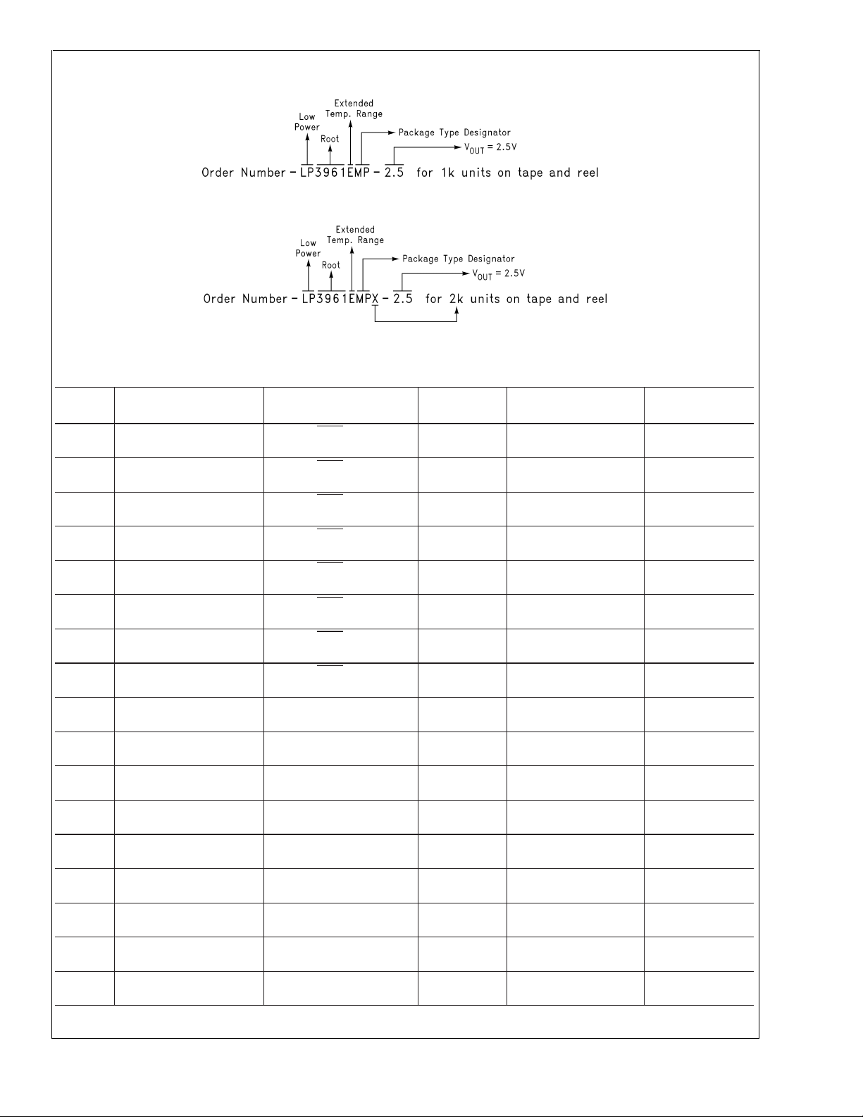
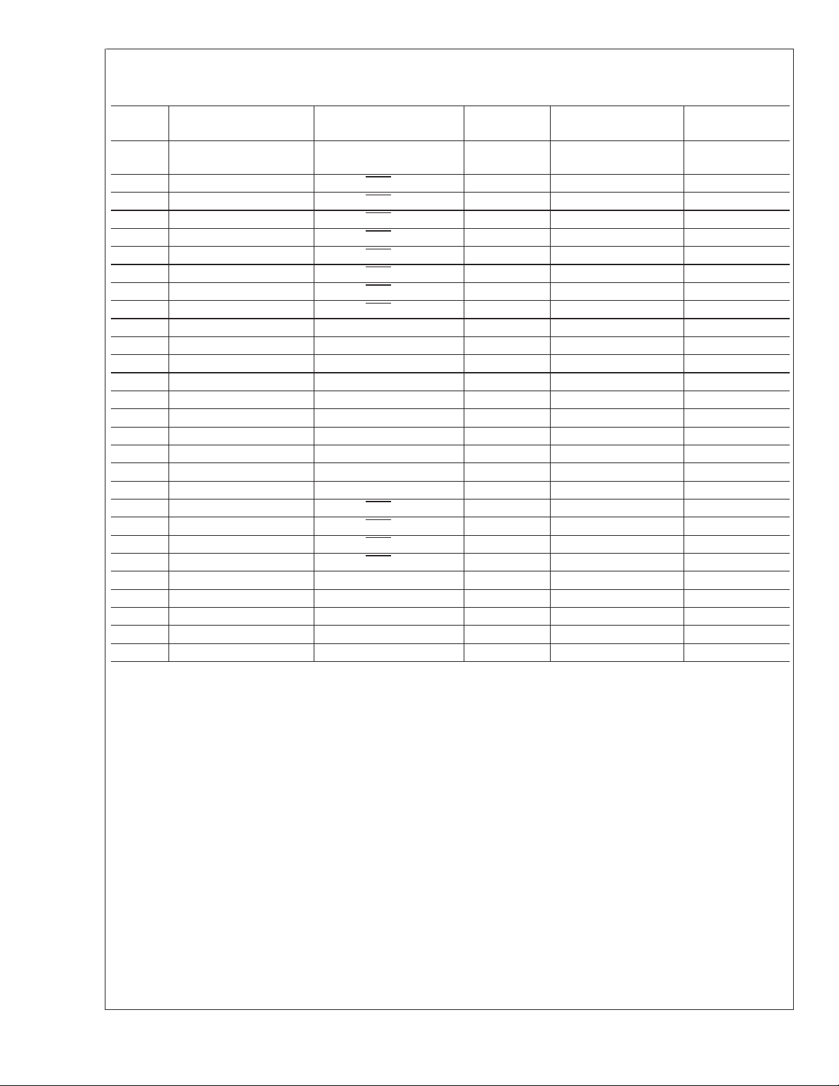
Ordering Information
Package Type Designator is ″MP″ for SOT223 package, ″T″ for TO220 package, and ″S″ for TO263 package.
TABLE 1. Package Marking and Ordering Information
LP3961/LP3964
DS101129-31
Output
Voltage
5.0 LP3961EMP-5.0 800mA, Error Flag
5.0 LP3961EMPX-5.0 800mA, Error Flag
3.3 LP3961EMP-3.3 800mA, Error Flag
3.3 LP3961EMPX-3.3 800mA, Error Flag
2.5 LP3961EMP-2.5 800mA, Error Flag
2.5 LP3961EMPX-2.5 800mA, Error Flag
1.8 LP3961EMP-1.8 800mA, Error Flag
1.8 LP3961EMPX-1.8 800mA, Error Flag
5.0 LP3964EMP-5.0 800mA, SENSE SOT223-5 LBUB 1000 units on
5.0 LP3964EMPX-5.0 800mA, SENSE SOT223-5 LBUB 2000 units on
3.3 LP3964EMP-3.3 800mA, SENSE SOT223-5 LBJB 1000 units on
3.3 LP3964EMPX-3.3 800mA, SENSE SOT223-5 LBJB 2000 units on
2.5 LP3964EMP-2.5 800mA, SENSE SOT223-5 LBHB 1000 units on
2.5 LP3964EMPX-2.5 800mA, SENSE SOT223-5 LBHB 2000 units on
1.8 LP3964EMP-1.8 800mA, SENSE SOT223-5 LBFB 1000 units on
1.8 LP3964EMPX-1.8 800mA, SENSE SOT223-5 LBFB 2000 units on
ADJ LP3964EMP-ADJ 800mA, ADJ SOT223-5 LBPB 1000 units on
Order Number Description
(Current, Option)
Package
Type
SOT223-5 LBSB 1000 units on
SOT223-5 LBSB 2000 units on
SOT223-5 LAZB 1000 units on
SOT223-5 LAZB 2000 units on
SOT223-5 LBBB 1000 units on
SOT223-5 LBBB 2000 units on
SOT223-5 LBAB 1000 units on
SOT223-5 LBAB 2000 units on
Package Marking Supplied As:
Tape and Reel
Tape and Reel
Tape and Reel
Tape and Reel
Tape and Reel
Tape and Reel
Tape and Reel
Tape and Reel
Tape and Reel
Tape and Reel
Tape and Reel
Tape and Reel
Tape and Reel
Tape and Reel
Tape and Reel
Tape and Reel
Tape and Reel
www.national.com5
Page 6
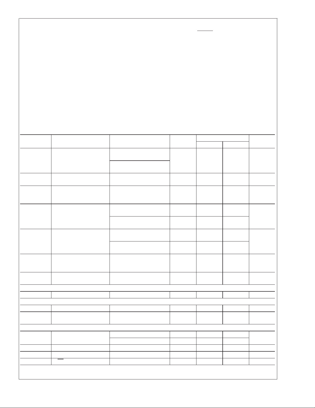
Ordering Information (Continued)
TABLE 1. Package Marking and Ordering Information (Continued)
Output
Voltage
LP3961/LP3964
ADJ LP3964EMPX-ADJ 800mA, ADJ SOT223-5 LBPB 2000 units on
5.0 LP3961ES-5.0 800mA, Error Flag
5.0 LP3961ESX-5.0 800mA, Error Flag
3.3 LP3961ES-3.3 800mA, Error Flag
3.3 LP3961ESX-3.3 800mA, Error Flag
2.5 LP3961ES-2.5 800mA, Error Flag
2.5 LP3961ESX-2.5 800mA, Error Flag
1.8 LP3961ES-1.8 800mA, Error Flag
1.8 LP3961ESX-1.8 800mA, Error Flag
5.0 LP3964ES-5.0 800mA, SENSE TO263-5 LP3964ES-5.0 Rail
5.0 LP3964ESX-5.0 800mA, SENSE TO263-5 LP3964ES-5.0 Tape and Reel
3.3 LP3964ES-3.3 800mA, SENSE TO263-5 LP3964ES-3.3 Rail
3.3 LP3964ESX-3.3 800mA, SENSE TO263-5 LP3964ES-3.3 Tape and Reel
2.5 LP3964ES-2.5 800mA, SENSE TO263-5 LP3964ES-2.5 Rail
2.5 LP3964ESX-2.5 800mA, SENSE TO263-5 LP3964ES-2.5 Tape and Reel
1.8 LP3964ES-1.8 800mA, SENSE TO263-5 LP3964ES-1.8 Rail
1.8 LP3964ESX-1.8 800mA, SENSE TO263-5 LP3964ES-1.8 Tape and Reel
ADJ LP3964ES-ADJ 800mA, ADJ TO263-5 LP3964ES-ADJ Rail
ADJ LP3964ESX-ADJ 800mA, ADJ TO263-5 LP3964ES-ADJ Tape and Reel
5.0 LP3961ET-5.0 800mA, Error Flag
3.3 LP3961ET-3.3 800mA, Error Flag
2.5 LP3961ET-2.5 800mA, Error Flag
1.8 LP3961ET-1.8 800mA, Error Flag
5.0 LP3964ET-5.0 800mA, SENSE TO220-5 LP3964ET-5.0 Rail
3.3 LP3964ET-3.3 800mA, SENSE TO220-5 LP3964ET-3.3 Rail
2.5 LP3964ET-2.5 800mA, SENSE TO220-5 LP3964ET-2.5 Rail
1.8 LP3964ET-1.8 800mA, SENSE TO220-5 LP3964ET-1.8 Rail
ADJ LP3964ET-ADJ 800mA, ADJ TO220-5 LP3964ET-ADJ Rail
Order Number Description
(Current, Option)
Package
Type
TO263-5 LP3961ES-5.0 Rail
TO263-5 LP3961ESX-5.0 Tape and Reel
TO263-5 LP3961ES-3.3 Rail
TO263-5 LP3961ES-3.3 Tape and Reel
TO263-5 LP3961ES-2.5 Rail
TO263-5 LP3961ES-2.5 Tape and Reel
TO263-5 LP3961ES-1.8 Rail
TO263-5 LP3961ES-1.8 Tape and Reel
TO220-5 LP3961ET-5.0 Rail
TO220-5 LP3961ET-3.3 Rail
TO220-5 LP3961ET-2.5 Rail
TO220-5 LP3961ET-1.8 Rail
Package Marking Supplied As:
Tape and Reel
www.national.com 6
Page 7
LP3961/LP3964
Absolute Maximum Ratings (Note 1)
If Military/Aerospace specified devices are required,
please contact the National Semiconductor Sales Office/
(Survival) Short Circuit Protected
I
OUT
Maximum Voltage for ERROR Pin
Maximum Voltage for SENSE Pin V
Distributors for availability and specifications.
Storage Temperature Range −65˚C to +150˚C
Lead Temperature
(Soldering, 5 sec.) 260˚C
ESD Rating (Note 3) 2 kV
Power Dissipation (Note 2) Internally Limited
Input Supply Voltage (Survival) −0.3V to +7.5V
Shutdown Input Voltage (Survival) −0.3V to V
+0.3V
IN
Operating Ratings
Input Supply Voltage (Operating) 2.5V to 7.0V
Shutdown Input Voltage
(Operating) −0.3V to V
Maximum Operating Current
(DC) 0.8A
Operating Junction Temp. Range −40˚C to +125˚C
Output Voltage (Survival), (Note
6), (Note 7) −0.3V to +7.5V
Electrical Characteristics
LP3961/LP3964
Limits in standard typeface are for TJ= 25˚C, and limits in boldface type apply over the full operating temperature
range. Unless otherwise specified: VIN=V
Symbol Parameter Conditions Typ(Note
Output Voltage
V
O
Tolerance
(Note 8)
∆V
OL
Output Voltage Line
Regulation (Note 8)
∆V
/
O
∆I
OUT
Output Voltage Load
Regulation
(Note 8)
V
-
IN
V
OUT
Dropout Voltage
(Note 10)
Ground Pin Current In
I
GND
Normal Operation
Mode
I
GND
Ground Pin Current In
Shutdown Mode
(Note 11)
I
O(PK)
Peak Output Current (Note 2) 1.5 1.2
SHORT CIRCUIT PROTECTION
I
SC
Short Circuit Current 2.8 A
OVER TEMPERATURE PROTECTION
Tsh(t) Shutdown Threshold 165 ˚C
Tsh(h) Thermal Shutdown
Hysteresis
SHUTDOWN INPUT
T
V
T
SDT
dOFF
dON
I
SD
Shutdown Threshold
Turn-off delay IL= 800 mA 20 µs
Turn-on delay IL= 800 mA 25 µs
SD Input Current VSD=V
+ 1V, IL= 10 mA, C
O(NOM)
=10µF, VSD=VIN-0.3V.
OUT
LP3961/4 (Note 5) Units
+1V<V
V
OUT
10 mA
3.135 ≤ V
V
+1V<V
OUT
4)
<
7.0V
IN
<
<
I
800 mA
L
≤ 7.0 for
IN
= 2.5V
V
OUT
<
7.0V, 0.02
IN
0
Min Max
-1.5
-3.0
0.06
<
<
I
10 mA
800 mA 0.02
L
0.08
I
=80mA 24 30
L
= 800 mA 240 300
I
L
=80mA 3 9
I
L
= 800 mA 4 14
I
L
≤ 0.2V 15 25
V
SD
1.1
10 ˚C
Output = High V
IN
VIN–0.3
Output = Low 0 0.2
IN
1nA
+1.5
+3.0
35
350
10
15
75
VIN+0.3V
+0.3V
OUT
+0.3V
IN
%
%
%
mV
mA
µA
A
V
www.national.com7
Page 8

Electrical Characteristics
LP3961/LP3964
Limits in standard typeface are for TJ= 25˚C, and limits in boldface type apply over the full operating temperature
range. Unless otherwise specified: VIN=V
Symbol Parameter Conditions Typ(Note
LP3961/LP3964
ERROR FLAG COMPARATOR
V
T
V
TH
V
EF(Sat)
Td Flag Reset Delay 1 µs
I
lk
I
max
AC PARAMETERS
PSRR Ripple Rejection
ρ
n(l/f
e
n
Note 1: Absolute maximum ratings indicate limits beyond which damage to the device may occur. Operating ratings indicate conditions for which the device is intended to be functional, but does notguaranteespecificperformancelimits.Forguaranteedspecificationsandtestconditions,see Electrical Charateristics.The guaranteed specifications apply only for the test conditions listed. Some performance characteristics may degrade when the device is not operated under the listed test
conditions.
Note 2: At elevated temperatures, devices must be derated based on package thermal resistance. The devices in TO220 package must be derated at θ
(with 0.5in
0.5in
Note 3: The human body model is a 100pF capacitor discharged through a 1.5kΩ resistor into each pin.
Note 4: Typical numbers are at 25˚C and represent the most likely parametric norm.
Note 5: Limits are 100% production tested at 25˚C. Limits over the operating temperature range are guaranteed through correlation using Statistical Quality Control
(SQC) methods. The limits are used to calculate National’s Average Outgoing Quality Level (AOQL).
Note 6: If used in a dual-supply system where the regulator load is returned to a negative supply, the LP396X output must be diode-clamped to ground.
Note 7: The output PMOS structure contains a diode between the V
if the voltage at the output terminal is forced to be higher than the voltage at the input terminal. This diode can typically withstand 200mA of DC current and 1Amp
of peak current.
Note 8: Output voltage line regulation is defined as the change in output voltage from the nominal value due to change in the input line voltage. Output voltage load
regulation is defined as the change in output voltage from the nominal value due to change in load current. The line and load regulation specification contains only
the typical number. However, the limits for line and load regulation are included in the output voltage tolerance specification.
Note 9: Error Flag threshold and hysteresis are specified as percentage of regulated output voltage.
Note 10: Dropout voltage is defined as the minimum input to output differential voltage at which the output drops 2% below the nominal value. Dropout voltage speci-
fication applies only to output voltages of 2.5V and above. For output voltages below 2.5V, the drop-out voltage is nothing but the input to output differential, since
the minimum input voltage is 2.5V.
Note 11: This specification has been tested for −40˚C ≤ T
2
2
, 1oz. copper area), junction-to-ambient. The devices in SOT223 package must be derated at θjA= 90˚C/W (with 0.5in2, 1oz. copper area), junction-to-ambient.
Threshold (Note 9) 10 516%
Threshold Hysteresis (Note 9) 5 28%
Error Flag Saturation I
Error Flag Pin Leakage
Current
Error Flag Pin Sink
Current
Output Noise Density f = 120Hz 0.8 µV
Output Noise Voltage
(rms)
, 1oz. copper area), junction-to-ambient (with no heat sink). The devices in the TO263 surface-mount package must be derated at θjA= 60˚C/W (with
(Continued)
+ 1V, IL= 10 mA, C
O(NOM)
=10µF, VSD=VIN-0.3V.
OUT
LP3961/4 (Note 5) Units
4)
= 100µA 0.02 0.1 V
sink
Min Max
1nA
V
= 0.5V (over
Error
1mA
temp.)
V
IN=VOUT
C
OUT
V
OUT
V
IN=VOUT
C
OUT
V
OUT
+ 1.5V
= 100uF
= 3.3V
+ 0.3V
= 100uF
= 3.3V
60
40
BW = 10Hz – 100kHz 150
BW = 300Hz – 300kHz 100
and V
IN
≤ 85˚C since the temperature rise of the device is negligible under shutdown conditions.
J
terminals. This diode is normally reverse biased. This diode will get forward biased
OUT
(rms)
= 50˚C/W
jA
dB
µV
www.national.com 8
Page 9

LP3961/LP3964
Typical Performance Characteristics Unless otherwise specified, V
C
=10µF, I
OUT
Drop-Out Voltage Vs Temperature for Different Load
Currents
Ground Pin Current Vs Input Voltage (VSD=VIN)
= 10mA, CIN=10µF, VSD=VIN, and TA= 25˚C.
OUT
DS101129-9
Drop-Out Voltage Vs Temperature for Different Output
Voltages (I
OUT
= 800mA)
Ground Pin Current Vs Input Voltage (VSD=100mV)
IN=VO(NOM)
+1V,V
DS101129-10
OUT
= 2.5V,
DS101129-11
Ground Current Vs Temperature (VSD=VIN)
DS101129-18
DS101129-15
Ground Current Vs Temperature (VSD=0V
DS101129-12
www.national.com9
Page 10

Typical Performance Characteristics Unless otherwise specified, V
C
OUT
=10µF, I
= 10mA, CIN=10µF, VSD=VIN, and TA= 25˚C. (Continued)
OUT
IN=VO(NOM)
+ 1V, V
OUT
= 2.5V,
Ground Pin Current Vs Shutdown Pin Voltage
LP3961/LP3964
Output Noise Density, V
OUT
= 2.5V
DS101129-16
Input Voltage Vs Output Voltage
Output Noise Density, V
OUT
=5V
DS101129-17
DS101129-13
DS101129-14
www.national.com 10
Page 11

Applications Information
Input Capacitor Selection
The LP3961 and LP3964 require a minimum input capacitance of 10µF between the input and ground pins to prevent
any impedance interactions with the supply. This capacitor
should be located very close to the V
can be of any type such as ceramic, tantalum, or aluminium.
Any good quality capacitor which has good tolerance over
temperature and frequency is recommended.
Output Capacitor Selection
The LP3961 and LP3964 require a minimum of 10µF capacitance between the output and ground pins for proper operation. LP3961 and LP3964 work best with Tantalum or Electrolytic capacitor. The output capacitor should have a good
tolerance over temperature, voltage, and frequency. Larger
capacitance provides better improved load dynamics and
noise performance. The output capacitor should be connected very close to the Vout pin.
Output Adjustment
An adjustable output device has output voltage range of
1.215V to 5.1V. To obtain a desired output voltage, the following equation can be used with R1 always a 10kΩ resistor.
For output stability, CFmust be between 68pF and 100pF.
Output Noise
Noise is specified in two waysSpot Noise or Output noise density is the RMS sum of all
noise sources, measured at the regulator output, at a specific frequency (measured with a 1Hz bandwidth). This type
of noise is usually plotted on a curve as a function of frequency.
Total output Noise or Broad-band noise is the RMS sum
of spot noise over a specified bandwidth, usually several decades of frequencies.
Attention should be paid to the units of measurement. Spot
noise is measured in units µV/
noise is measured in µV(rms).
The primary source of noise in low-dropout regulators is the
internal reference. In CMOS regulators, noise has a low fre-
√
Hz or nV/√Hz and total output
pin. This capacitor
IN
quency component and a high frequency component, which
depend strongly on the silicon area and quiescent current.
Noise can be reduced in two ways: by increasing the transistor area or by increasing the current drawn by the internal
reference. Increasing the area will decrease the chance of
fitting the die into a smaller package. Increasing the current
drawn by the internal reference increases the total supply
current (ground pin current). Using an optimized trade-off of
ground pin current and die size, LP3961/LP3964 achieves
low noise performance and low quiescent current operation.
The total output noise specification for LP3961/LP3964 is
presented in the Electrical Characteristics table. The Output
noise density at different frequencies is represented by a
curve under typical performance characteristics.
Short-Circuit Protection
The LP3961and LP3964 is short circuit protected and in the
event of a peak over-current condition, the short-circuit control loop will rapidly drive the output PMOS pass element off.
Once the power pass element shuts down, the control loop
will rapidly cycle the output on and off until the average
power dissipation causes the thermal shutdown circuit to respond to servo the on/off cycling to a lower frequency.
Please refer to the section on thermal information for power
dissipation calculations.
Error Flag Operation
The LP3961/LP3964 produces a logic low signal at the Error
Flag pin when the output drops out of regulation due to low
input voltage, current limiting, or thermal limiting. This flag
has a built in hysteresis. The timing diagram in
shows the relationship between the ERROR and the output
voltage. In this example, the input voltage is changed to
demonstrate the functionality of the Error Flag.
The internal Error flag comparator has an open drain output
stage. Hence, the ERROR pin should be pulled high through
a pull up resistor. Although the ERROR pin can sink current
of 1mA, this current is energy drain from the input supply.
Hence, the value of the pull up resistor should be in the
range of 100kΩ to 1MΩ. The ERROR pin must be con-
nected to ground if this function is not used. It should
also be noted that when the shutdown pin is pulled low, the
ERROR pin is forced to be invalid for reasons of saving
power in shutdown mode.
Figure 1
LP3961/LP3964
www.national.com11
Page 12

Applications Information (Continued)
LP3961/LP3964
Sense Pin
In applications where the regulator output is not very close to
the load, LP3964 can provide better remote load regulation
using the SENSE pin.
SENSE option. LP3961 regulates the voltage at the output
pin. Hence, the voltage at the remote load will be the regulator output voltage minus the drop across the trace resis-
Figure 2
depicts the advantage of the
FIGURE 1. Error Flag Operation
tance. For example, in the case of a 3.3V output, if the trace
resistance is 100mΩ, the voltage at the remote load will be
3.22V with 800mAmps of load current, I
regulates the voltage at the sense pin. Connecting the sense
pin to the remote load will provide regulation at the remote
load, as shown in
quired, the sense pin must be connected to the V
Figure 2
DS101129-7
. The LP3964
LOAD
. If the sense option pin is not re-
pin.
OUT
FIGURE 2. Improving remote load regulation using LP3964
Shutdown Operation
A CMOS Logic level signal at the shutdown ( SD) pin will
turn-off the regulator. Pin SD must be actively terminated
through a 10kΩ pull-up resistor for a proper operation. If this
www.national.com 12
DS101129-8
pin is driven from a source that actively pulls high and low
(such as a CMOS rail to rail comparator), the pull-up resistor
is not required. This pin must be tied to Vin if not used.
Page 13

Applications Information (Continued)
Dropout Voltage
The dropout voltage of a regulator is defined as the minimum
input-to-output differential required to stay within 2% of the
output voltage. The LP3961/LP3964 use an internal MOSFET with an Rds(on) of 240mΩ (typically). For CMOS LDOs,
the dropout voltage is the product of the load current and the
Rds(on) of the internal MOSFET.
Reverse Current Path
The internal MOSFET in LP3961and LP3964 has an inherent parasitic diode. During normal operation, the input voltage is higher than the output voltage and the parasitic diode
is reverse biased. However, if the output is pulled above the
input in an application, then current flows from the output to
the input as the parasitic diode gets forward biased. The output can be pulled above the input as long as the current in
the parasitic diode is limited to 200mA continuous and 1A
peak.
Maximum Output Current Capability
LP3961 and LP3964 can deliver a continuous current of
800mA over the full operating temperature range. A heatsink
may be required depending on the maximum power dissipation and maximum ambient temperature of the application.
Under all possible conditions, the junction temperature must
be within the range specified under operating conditions.
The total power dissipation of the device is given by:
P
=(VIN−V
D
where I
OUT)IOUT
is the operating ground current of the device
GND
(specified under Electrical Characteristics).
The maximum allowable temperature rise (T
on the maximum ambient temperature (T
cation, and the maximum allowable junction temperature(T
):
max
T
Rmax=TJmax−TAmax
The maximum allowable value for junction to ambient Thermal Resistance, θ
θ
JA=TRmax/PD
LP3961 and LP3964 are available in TO-220, TO-263, and
SOT-223 packages. The thermal resistance depends on
amount of copper area or heat sink, and on air flow. If the
maximum allowable value of θ
˚C/W for TO-220 package, ≥60 ˚C/W for TO-263 package,
and ≥ 140 ˚C/W for SOT-223 package, no heatsink is
needed since the package can dissipate enough heat to satisfy these requirements. If the value for allowable θ
below these limits, a heat sink is required.
+(VIN)I
GND
) depends
Rmax
) of the appli-
Amax
, can be calculated using the formula:
JA
calculated above is ≥ 60
JA
falls
JA
LP3961/LP3964
pends on method of attachment, insulator, etc. θ
between 1.5˚C/W to 2.5˚C/W. If the exact value is unknown,
2˚C/W can be assumed.
Heatsinking TO-263 and SOT-223 Packages
The TO-263 and SOT223 packages use the copper plane on
the PCB as a heatsink. The tab of these packages are soldered to the copper plane for heat sinking.
curve for the θ
of TO-263 package for different copper area
JA
Figure 3
sizes, using a typical PCB with 1 ounce copper and no solder
mask over the copper area for heat sinking.
DS101129-32
FIGURE 3. θJAvs Copper(1 Ounce) Area for TO-263
package
As shown in the figure, increasing the copper area beyond 1
square inch produces very little improvement. The minimum
value for θ
for the TO-263 packag mounted to a PCB is
JA
32˚C/W.
-
J
Figure 4
shows the maximum allowable power dissipation
for TO-263 packages for different ambient temperatures, assuming θ
is 35˚C/W and the maximum junction tempera-
JA
ture is 125˚C.
varies
CH
shows a
Heatsinking TO-220 Packages
The thermal resistance of a TO220 package can be reduced
by attaching it to a heat sink or a copper plane on a PC
board. If a copper plane is to be used, the values of θ
will
JA
be same as shown in next section for TO263 package.
The heatsink to be used in the application should have a
heatsink to ambient thermal resistance,
θ
HA≤θJA
In this equation, θ
tion to the surface of the heat sink and θ
sistance from the junction to the surface of the case. θ
about 3˚C/W for a TO220 package. The value for θ
− θCH− θJC.
CH
is the thermal resistance from the junc-
is the thermal re-
JC
JC
de-
CH
DS101129-33
FIGURE 4. Maximum power dissipation vs ambient
temperature for TO-263 package
Figure 5
shows a curve for the θJAof SOT-223 package for
different copper area sizes, using a typical PCB with 1 ounce
copper and no solder mask over the copper area for heat
is
sinking.
www.national.com13
Page 14

Applications Information (Continued)
LP3961/LP3964
DS101129-19
FIGURE 5. θJAvs Copper(1 Ounce) Area for SOT-223
package
The following figures show different layout scenarios for
SOT-223 package.
DS101129-22
FIGURE 8. SCENARIO C, θJA= 92˚C/W
DS101129-20
FIGURE 6. SCENARIO A, θJA= 148˚C/W
DS101129-21
FIGURE 7. SCENARIO B, θJA= 125˚C/W
DS101129-23
FIGURE 9. SCENARIO D, θJA= 83˚C/W
www.national.com 14
Page 15

Applications Information (Continued)
LP3961/LP3964
FIGURE 10. SCENARIO E, θJA= 77˚C/W
FIGURE 12. SCENARIO G, θJA= 113˚C/W
DS101129-24
DS101129-25
FIGURE 11. SCENARIO F, θJA= 75˚C/W
DS101129-26
www.national.com15
Page 16

Applications Information (Continued)
LP3961/LP3964
FIGURE 13. SCENARIO H, θJA= 79˚C/W
DS101129-27
www.national.com 16
Page 17

Applications Information (Continued)
LP3961/LP3964
FIGURE 14. SCENARIO I, θJA= 78.5˚C/W
DS101129-28
www.national.com17
Page 18

Physical Dimensions inches (millimeters) unless otherwise noted
LP3961/LP3964
TO220 5-lead, Molded, Stagger Bend Package (TO220-5)
NS Package Number T05D
For Order Numbers, refer to the “Ordering Information” section of this document.
www.national.com 18
Page 19

Physical Dimensions inches (millimeters) unless otherwise noted
LP3961/LP3964
TO263 5-Lead, Molded, Surface Mount Package (TO263-5)
NS Package Number TS5B
For Order Numbers, refer to the “Ordering Information” section of this document.
www.national.com19
Page 20

Physical Dimensions inches (millimeters) unless otherwise noted
SOT223, 5-Lead, Molded, Surface Mount Package (SOT223-5)
NS Package Number MA05C
For Order Numbers, refer to the “Ordering Information” section of this document.
LP3961/LP3964 800mA Fast Ultra Low Dropout Linear Regulators
LIFE SUPPORT POLICY
NATIONAL’S PRODUCTS ARE NOT AUTHORIZED FOR USE AS CRITICAL COMPONENTS IN LIFE SUPPORT
DEVICES OR SYSTEMS WITHOUT THE EXPRESS WRITTEN APPROVAL OF THE PRESIDENT AND GENERAL
COUNSEL OF NATIONAL SEMICONDUCTOR CORPORATION. As used herein:
1. Life support devices or systems are devices or
systems which, (a) are intended for surgical implant
into the body, or (b) support or sustain life, and
whose failure to perform when properly used in
accordance with instructions for use provided in the
labeling, can be reasonably expected to result in a
significant injury to the user.
National Semiconductor
Corporation
Americas
Tel: 1-800-272-9959
Fax: 1-800-737-7018
Email: support@nsc.com
www.national.com
National does not assume any responsibility for use of any circuitry described, no circuit patent licenses are implied and National reserves the right at any time without notice to change said circuitry and specifications.
National Semiconductor
Europe
Fax: +49 (0) 180-530 85 86
Email: europe.support@nsc.com
Deutsch Tel: +49 (0) 69 9508 6208
English Tel: +44 (0) 870 24 0 2171
Français Tel: +33 (0) 1 41 91 8790
2. A critical component is any component of a life
support device or system whose failure to perform
can be reasonably expected to cause the failure of
the life support device or system, or to affect its
safety or effectiveness.
National Semiconductor
Asia Pacific Customer
Response Group
Tel: 65-2544466
Fax: 65-2504466
Email: ap.support@nsc.com
National Semiconductor
Japan Ltd.
Tel: 81-3-5639-7560
Fax: 81-3-5639-7507
Page 21

Copyright © Each Manufacturing Company.
All Datasheets cannot be modified without permission.
This datasheet has been download from :
www.AllDataSheet.com
100% Free DataSheet Search Site.
Free Download.
No Register.
Fast Search System.
www.AllDataSheet.com
 Loading...