

LP3950
Color LED Driver with Audio Synchronizer
LP3950 Color LED Driver with Audio Synchronizer
February 2005
General Description
The LP3950 is a color LED driver with a built-in audio
synchronization feature for any analog audio input such as
polyphonic ring tones and MP3 music. LEDs can be synchronized to an audio signal with two methods - amplitude
and frequency. Also several fine tuning options are available
for differentiation purposes. The chip also has an unique
AGC (Automatic Gain Control) feature which tracks the input
signal level and automatically adjusts the gain to an optimal
value.
The LP3950 has a high efficiency magnetic DC/DC converter with programmable output voltage and switching frequency. The converter has high output current capability so it
is also able to drive flash LEDs in camera phone applications.
The LP3950 is similar to LP3933 and LP3936 in that the
color LEDs (or RGB LEDs) can also be programmed to
generate light patterns (programmable color, intensity, on/off
timing, slope and blinking cycle).
All functions are software controllable through a SPI or I
compatible interface but the device also supports one pin
control for enabling predefined (default) audio synchronization mode.
2
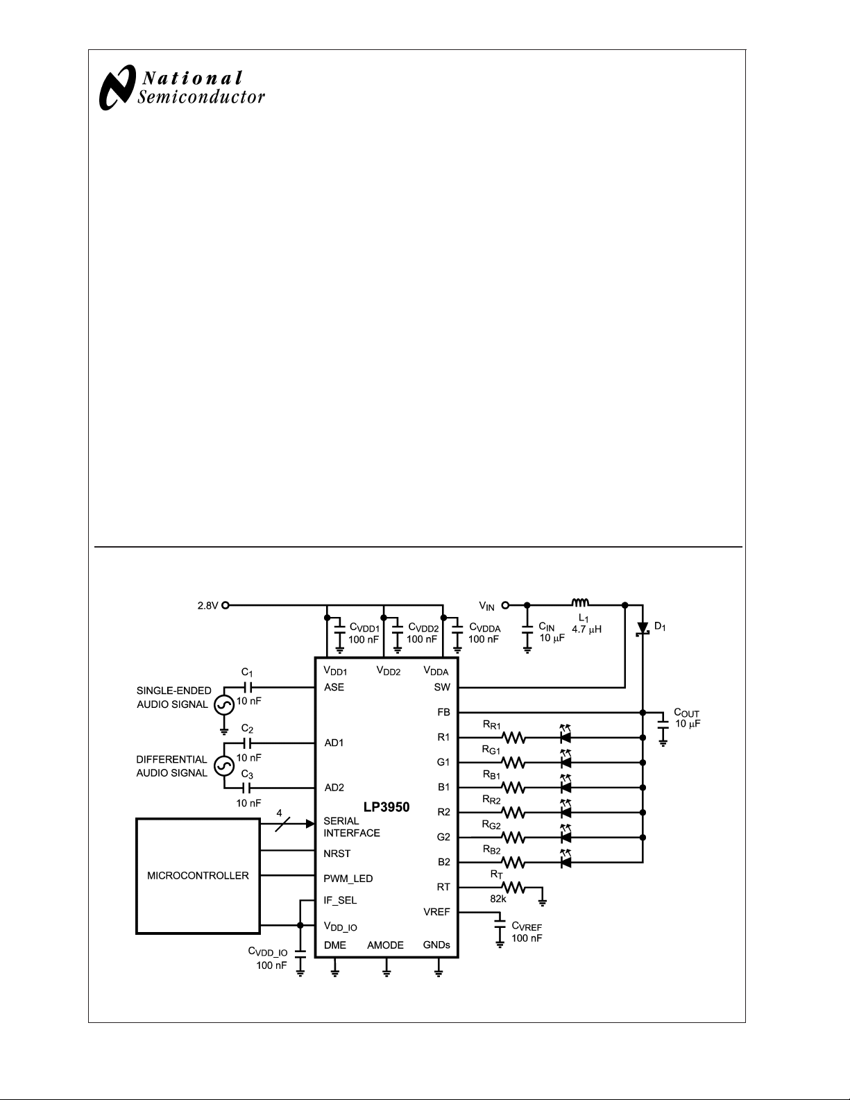
Typical Application
Features
n Audio synchronization for color LEDs with two modes:
Amplitude and Frequency
n Programmable frequency and amplitude response with
tracking speed control
n Automatic gain control or selectable gain for input signal
optimization
n RGB pattern generator similar to LP3933/LP3936
n Magnetic DC-DC boost converter with programmable
boost output voltage
n Selectable SPI or I
n One pin default enable for non-serial interface users.
One pin selector for synchronization mode
n Space efficient 32-pin thin CSP laminate package
2
C compatible interface
Applications
n Cellular phones
n MP3/CD/minidisc players
n Toys
C
20129301
© 2005 National Semiconductor Corporation DS201293 www.national.com
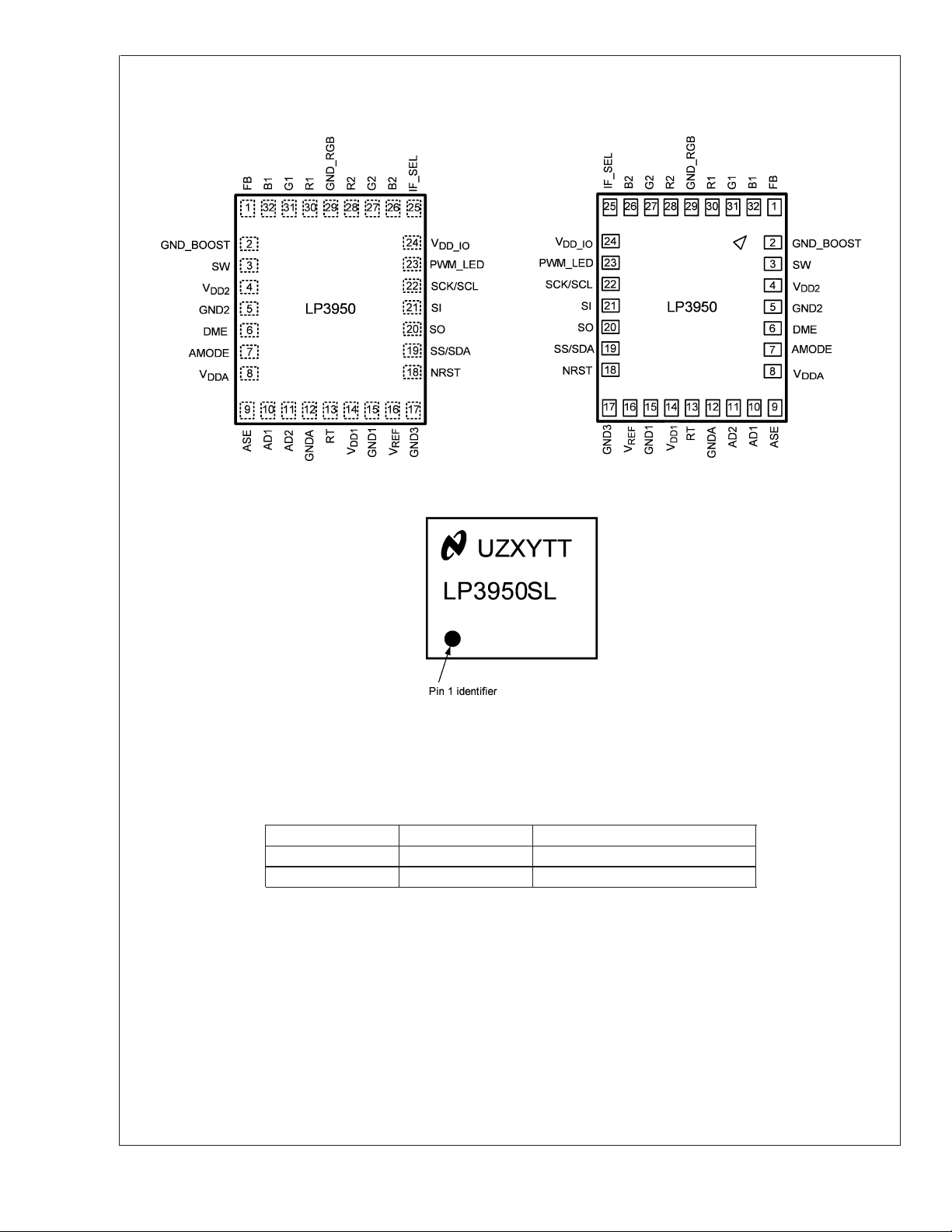
Connection Diagrams and Package Mark Information
LP3950
32-Lead Thin CSP Package, 4.5 x 5.5 x 0.8 mm, 0.5 mm Pitch
See NS Package Number SLD32A
Top View
20129302
20129304
Note: The actual physical placement of the package marking will vary from part to part. The package marking “XY” designates the date code. “UZ” and “TT” are NSC
internal codes for die manufacturing and assembly traceability. Both will vary considerably.
Bottom View
20129303
Package Mark — Top View
Ordering Information
Order Number Package Marking Supplied As
LP3950SL LP3950SL 1000 units, Tape-and-Reel
LP3950SLX LP3950SL 2500 units, Tape-and-Reel
www.national.com 2
Pin Description
Pin # Name Type Description
1 FB Input Boost converter feedback.
2 GND_BOOST Ground Power switch ground.
3 SW Output Open drain, boost converter power switch.
4V
DD2
5 GND2 Ground Ground return for V
6 DME Logic Input Default mode enable (internal pull down 1 MΩ).
7 AMODE Logic Input Audio mode selection (internal pull down 1 MΩ).
8V
DDA
9 ASE Input Analog audio input, single-ended.
10 AD1 Input Analog audio input, differential.
11 AD2 Input Analog audio input, differential.
12 GNDA Ground Ground for analog audio inputs.
13 RT Input Oscillator resistor.
14 V
DD1
15 GND1 Ground Ground.
16 V
REF
17 GND3 Ground Ground.
18 NRST Logic Input Low active reset input.
19 SS/SDA Logic I/O SPI slave select/ I
20 SO Logic Output SPI serial data output.
21 SI Logic Input SPI serial data input.
22 SCK/SCL Logic Input SPI/ I
23 PWM_LED Logic Input Direct PWM control for LEDs.
24 V
DDIO
25 IF_SEL Logic Input SPI/I
26 B2 Output Open drain output, blue LED2.
27 G2 Output Open drain output, green LED2.
28 R2 Output Open drain output, red LED2.
29 GND_RGB Ground RGB driver ground.
30 R1 Output Open drain output, red LED1.
31 G1 Output Open drain output, green LED1.
32 B1 Output Open drain output, blue LED1.
Power Supply voltage for internal digital circuits.
(internal digital).
DD2
Power Supply voltage for audio circuits.
Power Supply voltage for internal analog circuits.
Output Internal reference bypass capacitor.
2
C data line.
2
C clock.
Power Supply voltage for logic IO signals.
2
C select (IF_SEL=1inSPImode).
LP3950
www.national.com3

Absolute Maximum Ratings (Notes 1,
2)
LP3950
If Military/Aerospace specified devices are required,
please contact the National Semiconductor Sales Office/
Distributors for availability and specifications.
Maximum Lead Temperature 260˚C
(Reflow soldering, 3 times) (Note 7)
ESD Rating (Note 8)
Human Body Model: 2 kV
Machine Model: 200V
V (SW, FB, R1–2, G1–2, B1–2)
(Notes 3, 4) −0.3V to +7.2V
V
DD1,VDD2,VDDIO,VDDA
−0.3V to +6.0V
Voltage on ASE, AD1, AD2 −0.3V to
+0.3V with 6.0V max
V
DD1
Voltage on Logic Pins −0.3V to V
DD_IO
+0.3V with 6.0V max
I (R1, G1, B1, R2, G2, B2)
150 mA
(Note 5)
I(V
)10µA
REF
Continuous Power Dissipation
Internally Limited
Operating Ratings (Notes 1, 2)
V (SW, FB, R1–2, G1– 2, B1–2) 0V to 6.0V
V
DD1,VDD2,VDDA
V
DDIO
Voltage on ASE, AD1, AD2 0.1V to V
Recommended Load Current 0 mA to 300 mA
Junction Temperature (T
Ambient Temperature (T
(Note 9) −40˚C to +85˚C
(Note 4) 2.7V to 2.9V
1.65V to V
) Range −40˚C to +125˚C
J
) Range
A
(Note 6)
Junction Temperature (T
Storage Temperature Range −65˚C to +150˚C
) 125˚C
J-MAX
Thermal Properties
Junction-to-Ambient Thermal Resistance 72˚C/W
(θ
), SLD32A Package (Note 10)
JA
Electrical Characteristics (Notes 2, 11)
Limits in standard typeface are for TJ= +25˚C. Limits in boldface type apply over the operating ambient temperature range
(−40˚C ≤ T
C
VDD2=CVDDA=CVDDIO
≤ +85˚C). Unless otherwise noted, specifications apply to Figure 1 with: V
A
= 100 nF, C
OUT=CIN
= 10 µF, C
= 100 nF, L1= 4.7 µH and f
VREF
DD1=VDD2=VDDA
BOOST
Symbol Parameter Condition Min Typ Max Units
I
VDD
I
VDDIO
I
VDDA
Standby Supply Current
(V
DD1+VDD2+VDDA
current)
No-Load Supply Current
(V
DD1+VDD2+VDDA
current, boost
off)
Full Load Supply Current
(V
DD1+VDD2+VDDA
current, boost
on)
(Note 13)
V
Supply Current 1.0 MHz SCK Frequency
DDIO
Audio Circuitry Supply Current
NSTBY = L (register)
SCK, SS, SI, NRST = H
NSTBY = H (reg.)
EN_BOOST = L (reg.)
SCK, SS, SI, NRST = H
NSTBY = H (reg.)
EN_BOOST = H (reg.)
SCK, SS, SI, NRST = H
All Outputs Active
=50pFatSOPin
C
L
INPUT_SEL = [10] (register) 550 µA
(Note 14)
V
REF
Reference Voltage(Note 15) I
≤ 1.0 nA Only for Test
REF
1.230 V
Purpose
Note 1: Absolute Maximum Ratings indicate limits beyond which damage to the component may occur. Operating Ratings are conditions under which operation of
the device is guaranteed. Operating Ratings do not imply guaranteed performance limits. For guaranteed performance limits and associated test conditions, see the
Electrical Characteristics tables.
Note 2: All voltages are with respect to the potential at the GND pins (GND1–3, GND_BOOST, GND_RGB, GNDA).
Note 3: Battery/Charger voltage should be above 6.0V no more than 10% of the operational lifetime.
Note 4: Voltage tolerance of LP3950 above 6.0V relies on fact that V
not available (ON) at all conditions, National Semiconductor does not guarantee any parameters or reliability for this device. Also, V
at the same electric potential.
Note 5: The total load current of the boost converter should be limited to 300 mA.
Note 6: Internal thermal shutdown circuitry protects the device from permanent damage. Thermal shutdown engages at T
140˚C (typ.).
Note 7: For detailed package and soldering specifications and information, please refer to National Semiconductor Application Note 1125: Laminate CSP/FBGA.
Note 8: The Human body model is a 100 pF capacitor discharged through a 1.5 kΩ resistor into each pin. The machine model is a 200 pF capacitor discharged
directly into each pin. MIL-STD-883 3015.7
DD1,VDD2
and V
(2.8V) are available (ON) at all conditions. If V
DDA
= 160˚C (typ.) and disengages at TJ=
J
= 2.8V, C
= 2.0 MHz (Note 12).
1 5 µA
300 400 µA
850 µA
20 µA
DD1,VDD2
DD1,VDD2
and V
DD1
VDD1
and V
DDA
DD1,2
- 0.1V
DDA
must be
V
=
are
www.national.com 4

Electrical Characteristics (Notes 2, 11) (Continued)
Note 9: In applications where high power dissipation and/or poor package thermal resistance is present, the maximum ambient temperature may have to be
derated. Maximum ambient temperature (T
dissipation of the device in the application (P
following equation: T
Note 10: Junction-to-ambient thermal resistance is highly application and board-layout dependent. In applications where high maximum power dissipation exists,
special care must be paid to thermal dissipation issues in board design.
Note 11: Min and Max limits are guaranteed by design, test, or statistical analysis. Typical numbers are not guaranteed, but do represent the most likely norm.
Note 12: Low-ESR Surface-Mount Ceramic Capacitors are used in setting electrical characteristics.
Note 13: Audio block inactive.
Note 14: In single-ended and in differential mode one audio buffer only is active and I
Note 15: V
A-MAX=TJ-MAX-OP
pin (Bandgap reference output) is for internal use only. A capacitor should always be placed between V
REF
) is dependent on the maximum operating junction temperature (T
A-MAX
), and the junction-to ambient thermal resistance of the part/package in the application (θJA), as given by the
D-MAX
−(θJAxP
D-MAX
).
will be reduced by 90 µA (typ).
VDDA
= 125˚C), the maximum power
J-MAX-OP
and GND1.
REF
LP3950
www.national.com5
LP3950
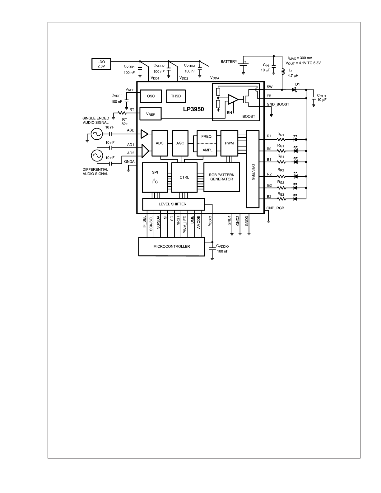
Block Diagram
20129305
FIGURE 1. LP3950 Block Diagram
Modes of Operation
RESET: In the RESET mode all the internal registers are reset to the default values. RESET is entered always if
input NRST is LOW or internal Power On Reset is active.
STANDBY: The STANDBY mode is entered if the register bit NSTBY is LOW and RESET is not active. This is the low
power consumption mode, when all the circuit functions are disabled. Registers can be written in this mode
and the control bits are effective immediately after start up.
STARTUP: INTERNAL STARTUP SEQUENCE powers up all the needed internal blocks (V
ensure the correct oscillator initialization, a 10 ms delay is generated by the internal state-machine. Thermal
shutdown (THSD) disables the chip operation and Startup mode is entered until no thermal shutdown event
is present.
BOOST STARTUP: Soft start for boost output is generated in the BOOST STARTUP mode. In this mode the boost output is
raised in PFM mode during the 10 ms delay generated by the state-machine. All RGB outputs are off during
the 10 ms delay to ensure smooth startup. The Boost startup is entered from Internal Startup Sequence if
EN_BOOST is HIGH or from Normal mode when EN_BOOST is written HIGH.
NORMAL: During the NORMAL mode the user controls the chip using the control registers. Registers can be written
in any sequence and any number of bits can be altered in a register within one write cycle . If the default
mode is selected, default control register values are used.
, oscillator, etc.). To
REF
www.national.com 6

Modes of Operation (Continued)
LP3950
20129306
Logic Interface Characteristics
(1.80V ≤ V
ambient temperature range (−40˚C ≤ T
Symbol Parameter Conditions Min Typ Max Units
LOGIC INPUTS SS, SI, SCK/SCL, PWM_LED, IF_SEL
V
IL
V
IH
I
I
f
SCL
LOGIC OUTPUT SO
V
OL
V
OH
I
L
LOGIC I/O SDA
V
OL
LOGIC INPUTS DME, AMODE (Internal pull down 1 MΩ)
V
IL
V
IH
DDIO
≤ V
V). Limits in standard typeface are for TJ= +25˚C. Limits in boldface type apply over the operating
DD1,2
≤ +85˚C).
A
Input Low Level 0.5 V
Input High Level V
− 0.5 V
DDIO
Logic Input Current −1.0 1.0 µA
Clock Frequency I2C Mode 400 kHz
SPI Mode 8 MHz
Output Low Level ISO= 3.0 mA 0.3 0.5 V
Output High Level ISO= −3.0 mA V
− 0.5 V
DDIO
− 0.3 V
DDIO
Output Leakage Current VSO= 2.8V 1.0 µA
Output Low Level I
= 3.0 mA 0.3 0.5 V
SDA
Input Low Level 0.5 V
Input High Level V
− 0.5 V
DDIO
www.national.com7

Logic Interface Characteristics (Continued)
(1.80V ≤ V
LP3950
ambient temperature range (−40˚C ≤ T
Symbol Parameter Conditions Min Typ Max Units
LOGIC INPUTS DME, AMODE (Internal pull down 1 MΩ)
I
I
DDIO
≤ V
V). Limits in standard typeface are for TJ= +25˚C. Limits in boldface type apply over the operating
DD1,2
≤ +85˚C).
A
Logic Input Current −1.0 6.0 µA
Logic Interface Characteristics, Low I/O Voltage
(1.65V ≤ V
Symbol Parameter Conditions Min Typ Max Units
LOGIC INPUTS SCL, PWM_LED, IF_SEL
V
IL
V
IH
I
I
f
SCL
LOGIC I/O SDA
V
OL
LOGIC INPUTS DME, AMODE (Internal pull down 1 MΩ)
V
IL
V
IH
I
I
<
1.80V) . I2C compatible interface only.
DDIO
Input Low Level 0.35 V
Input High Level V
− 0.35 V
DDIO
Logic Input Current −1.0 1.0 µA
Clock Frequency I2C Mode 200 kHz
Output Low Level I
= 3.0 mA 0.3 0.5 V
SDA
Input Low Level 0.35 V
Input High Level V
− 0.35 V
DDIO
Logic Input Current −1.0 6.0 µA
Logic Input NRST Characteristics
(1.65V ≤ V
Symbol Parameter Conditions Min Typ Max Units
V
IL
V
IH
I
I
t
NRST
DDIO
≤ V
DD1,2
V).
Input Low Level 0.5 V
Input High Level 1.3 V
Logic Input Current −1.0 1.0 µA
Reset Pulse Width Note: Guaranteed by
design
10 µs
Control Interface
The LP3950 supports three different interface modes:
1) SPI interface (4 wire, serial)
2
2) I
C compatible interface (2 wire, serial)
3) Direct enable (2 wire, enable lines)
IF_SEL Interface Pin Configuration Comment
HIGH SPI SCK
SI
SO
SS
2
LOW I
C Compatible SCL
SDA
SI
SO
(clock)
(data in)
(data out)
(chip select)
(clock)
(data in/out)
2
address)
(I
(NC)
User can define the serial interface by the IF_SEL pin. The
following table shows the pin configuration for both interface
modes. Note that the pin configurations will be based on the
status of the IF_SEL pin.
Use pull up resistor for SCL.
Use pull up resistor for SDA.
SI HIGH→address is 51’h;
SI LOW→address is 50’h;
Unused pin SO can be left unconnected.
SPI Interface
The transmission consists of 16-bit write and read cycles.
One cycle consists of seven address bits, one read/write
(R/W) bit and eight data bits. R/W bit high state defines a
write cycle and low defines a read cycle. SO output is
normally in high-impedance state and it is active only during
www.national.com 8
when data is sent out during a read cycle. A pull-up or
pull-down resistor may be needed for SO line if a floating
logic signal can cause unintended current consumption in
the circuitry.
The address and data are transmitted Most Significant Byte
(MSB) first. The Slave Select signal (SS) must be low during
the cycle transmission. SS resets the interface when high

SPI Interface (Continued)
and it has to be taken high between successive cycles. Data
FIGURE 2. SPI Write Cycle
LP3950
is clocked in on the rising edge of the SCK clock signal, while
data is clocked out on the falling edge of SCK.
20129307
FIGURE 3. SPI Read Cycle
FIGURE 4. SPI Timing Diagram
20129308
20129309
www.national.com9
LP3950
SPI Timing Parameters
V
DD1=VDD2=VDDA
Symbol Parameter
= 2.70V to 2.90V, V
= 1.80V to V
DDIO
V
DD1,2
Min Max
Limit
1 Cycle Time 80 ns
2 Enable Lead Time 40 ns
3 Enable Lag Time 40 ns
4 Clock Low Time 40 ns
5 Clock High Time 40 ns
6 Data Setup Time 0 ns
7 Data Hold Time 20 ns
8 Data Access Time 27 ns
9 Output Disable Time 27 ns
10 Output Data Valid 37 ns
11 Output Data Hold Time 0 ns
12 SS Inactive Time 15 ns
Note: Data guaranteed by design.
Units
I2C Compatible Interface
I2C SIGNALS
2
C compatible mode, the LP3950 pin SCL is used for the
In I
2
C clock and the SDA pin is used for the I2C data. Both
I
these signals need a pull-up resistor according to I
fication. The values of the pull-up resistors are determined
A
by the capacitance of the bus (typ.
specifications are shown in Table I
1.8k). Signal timing
2
C Timing Parameters .
Unused pin SO can be left unconnected and pin SI must be
2
C START AND STOP CONDITIONS
I
START and STOP bits classify the beginning and the end of
2
C session. START condition is defined as SDA signal
the I
transition from HIGH to LOW while SCL line is HIGH. STOP
condition is defined as the SDA transition from LOW to HIGH
while SCL is HIGH. The I
2
C master always generates
2
C speci-
FIGURE 5. I2C Signals: Data Validity
connected to V
rate is 400 kbit/s (V
interface can be used down to 1.65 V
or GND (address selector). Maximum bit
DDIO
DDIO
1.80V to V
V). I2C compatible
DD1,2
with maximum bit
DDIO
rate of 200 kbit/s.
2
I
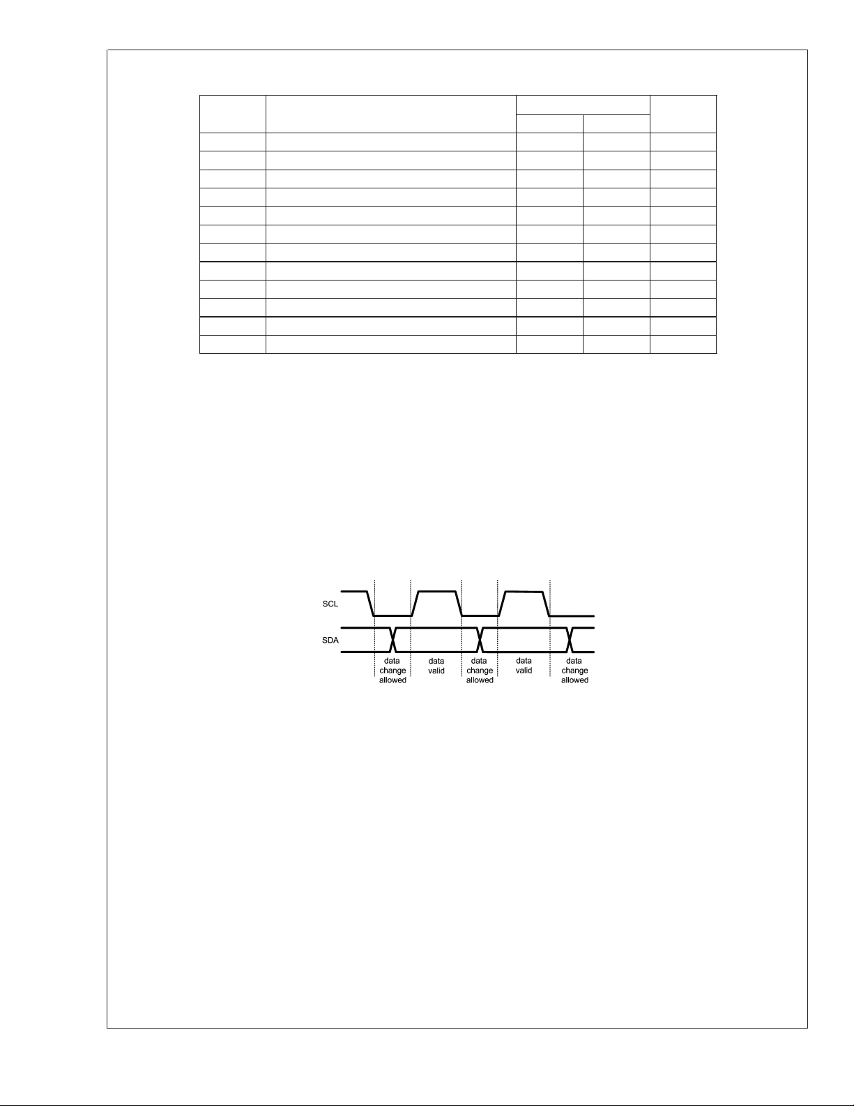
C DATA VALIDITY
The data on the SDA line must be stable during the HIGH
period of the clock signal (SCL). In other words, state of the
data line can only be changed when CLK is LOW.
20129310
2
START and STOP bits. The I
after START condition and free after STOP condition. During
data transmission, the I
C bus is considered to be busy
2
C master can generate repeated
START conditions. First START and repeated START conditions are equivalent, function-wise.
www.national.com 10

I2C Compatible Interface (Continued)
FIGURE 6. Start and Stop Conditions
TRANSFERRING DATA
Every byte put on the SDA line must be eight bits long, with
the most significant bit (MSB) being transferred first. Each
byte of data has to be followed by an acknowledge bit. The
acknowledge related clock pulse is generated by the master.
The transmitter releases the SDA line (HIGH) during the
acknowledge clock pulse. The receiver must pull down the
SDA line during the 9th clock pulse, signifying an acknowledge. A receiver which has been addressed must generate
an acknowledge after each byte has been received.
20129311
2
After the START condition, the I
C master sends a chip
address. This address is seven bits long followed by an
eighth bit which is a data direction bit (R/W). The LP3950
address is 50’h or 51’h. The selection of the address is done
by connecting SI pin to V
(51 hex) or GND (50 hex). For
DDIO
the eighth bit, a “0” indicates a WRITE and a “1” indicates a
READ. The second byte selects the register to which the
data will be written. The third byte contains data to write to
the selected register.
LP3950
FIGURE 7. I2C Chip Address
w = write (SDA = “0”)
r = read (SDA = “1”)
ack = acknowledge (SDA pulled down by either master or slave)
rs = repeated start
id = chip address, 50’h or 51’h for LP3950.
FIGURE 8. I2C Write Cycle
When a READ function is to be accomplished, a WRITE
function must precede the READ function, as shown in
Figure 9 .
20129312
20129313
www.national.com11

I2C Compatible Interface (Continued)
LP3950
20129314
FIGURE 9. I2C Read Cycle
20129341
FIGURE 10. I2C Timing Diagram
2
C Timing Parameters
I
(V
DD1=VDD2=VDDA
= 2.70V to 2.90V, V
= 1.65V to V
DDIO
DD1,2
V)
Symbol Parameter Limit Units
Min Max
1 Hold Time (repeated) START Condition 0.6 µs
2 Clock Low Time (1.65V ≤ V
2 Clock Low Time (1.80V ≤ V
3 Clock High Time (1.65V ≤ V
3 Clock High Time (1.80V ≤ V
<
1.80V) 3.2 µs
DDIO
DDIO
DDIO
DDIO
≤ V
V) 1.3 µs
DD1,2
<
1.80V) 1200 ns
≤ V
V) 600 ns
DD1,2
4 Setup Time for a Repeated START Condition 600 ns
5 Data Hold Time (data output, delay generated by LP3950) 300 900 ns
5 Data Hold Time (data input) 0 900 ns
6 Data Setup Time 100 ns
7 Rise Time of SDA and SCL 20+0.1C
8 Fall Time of SDA and SCL 15+0.1C
b
b
300 ns
300 ns
9 Set-up Time for STOP condition 600 ns
10 Bus Free Time between a STOP and a START Condition 1.3 µs
C
b
Capacitive Load Parameter for Each Bus Line.
10 200 ns
Load of One Picofarad Corresponds to One Nanosecond.
NOTE: Data guaranteed by design
www.national.com 12

Magnetic Boost DC/DC Converter
The boost DC/DC converter generates a 4.1V–5.3V output voltage to drive LEDs from a single Li-Ion battery (3.0V to 4.5V). The
output voltage is controlled with an eight-bit register in nine steps. The converter is a magnetic switching PWM mode DC/DC
converter with a current limit. The converter has three options for switching frequency, 1.0 MHz, 1.67 MHz and 2.0 MHz (default),
when the timing resistor RT is 82 kΩ.
The LP3950 boost converter uses an unique pulse-skipping elimination method to stabilize the noise spectrum. Even with light
load or no load a minimum length current pulse is fed to the inductor. An internal active load is used to remove the excess charge
from the output capacitor when needed (Note 16). The boost converter should be disabled when there is no load to avoid idle
current consumption.
The topology of the magnetic boost converter is called CPM control, current programmed mode, where the inductor current is
measured and controlled with the feedback. The output voltage control changes the resistor divider in the feedback loop.
Figure 11 shows the boost topology with the protection circuitry. Four different protection schemes are implemented:
1. Over voltage protection, limits the maximum output voltage
— Keeps the output below breakdown voltage
— Prevents boost operation if the battery voltage is much higher than desired output
2. Over current protection, limits the maximum inductor current
— Voltage over switching NMOS is monitored; too high voltages turn the switch off
3. Feedback (FB) protection for no connection
4. Duty cycle limit function, done with digital control
Note 16: When the battery voltage is close to the output voltage, the output voltage may rise slightly over programmed value if the load on output is small and
pulse-skipping elimination is active.
LP3950
20129315
FIGURE 11. Boost Converter Functional Block Diagram
Magnetic Boost DC/DC Converter Electrical Characteristics
Limits in standard typeface are for TJ= +25˚C. Limits in boldface type apply over the operating ambient temperature range
(−40˚C ≤ T
C
VDD2=CVDDA=CVDDIO
≤ +85˚C). Unless otherwise noted, specifications apply to Figure 1 with: V
A
= 100 nF, C
OUT=CIN
= 10 µF, C
= 100 nF, L1= 4.7 µH and f
VREF
DD1=VDD2=VDDA
BOOST
Symbol Parameter Conditions Min Typ Max Units
I
LOAD
V
OUT
Load Current 3.0V ≤ VIN≤ 4.5V
= 5.0V
V
OUT
Output Voltage Accuracy
(FB Pin)
Output Voltage
(FB Pin)
1.0 mA ≤ I
3.0V ≤ V
V
OUT
1.0 mA ≤ I
3.0V
LOAD
≤ 4.5V
IN
= 5.0V (target value), autoload OFF
LOAD
<
<
V
5.0V + V
IN
0 300 mA
≤ 300 mA
−5 +5 %
≤ 300 mA
(SCHOTTKY),
autoload OFF
1.0 mA ≤ I
>
5V+V
V
IN
LOAD
(SCHOTTKY)
≤ 300 mA
VIN–V
= 2.8V, C
VDD1
=
= 2.0 MHz (Note 12).
5.0 V
(SCHOTTKY)
www.national.com13
V

Magnetic Boost DC/DC Converter Electrical Characteristics (Continued)
Limits in standard typeface are for TJ= +25˚C. Limits in boldface type apply over the operating ambient temperature range
LP3950
(−40˚C ≤ T
C
VDD2=CVDDA=CVDDIO
≤ +85˚C). Unless otherwise noted, specifications apply to Figure 1 with: V
A
= 100 nF, C
OUT=CIN
= 10 µF, C
= 100 nF, L1= 4.7 µH and f
VREF
DD1=VDD2=VDDA
= 2.0 MHz (Note 12).
BOOST
= 2.8V, C
VDD1
Symbol Parameter Conditions Min Typ Max Units
RDS
f
PWF
Switch ON Resistance V
ON
PWM Mode Switching
Frequency
Frequency Accuracy 2.7 ≤ VDD
= 2.8V, ISW= 0.5A 0.4 0.7 Ω
DD1,2
RT=82kΩ
freq_sel[2:0] = 1XX
≤ 2.9 −6
1,2
2.0 MHz
±
3+6
RT=82kΩ −9 +9
t
PULSE
Switch Pulse Minimum
No Load 25 ns
Width
t
STARTUP
I
CL_OUT
Startup Time 15 ms
SW Pin Current Limit 700 800 900
500 1000
Boost Standby Mode
User can set the boost converter to STANDBY mode by writing the register bit EN_BOOST low when there is no load to avoid
idle current consumption. When EN_BOOST is written high, the converter starts in PFM (Pulse Frequency Modulation) mode for
10 ms and then goes to PWM (Pulse Width Modulation ) mode. All RGB outputs are off during the 10 ms delay.
Boost Output Voltage Control
User can control the boost output voltage by eight-bit boost output voltage register according to the following table.
=
%
mA
BOOST[7:0]
Register 0D’h
Binary Hex
0000 0000 00 4.10
0000 0001 01 4.25
0000 0011 03 4.40
0000 0111 07 4.55
BOOST Output
Voltage
(typical)
BOOST[7:0]
Register 0D’h
Binary Hex
BOOST Output
Voltage
(typical)
0001 1111 1F 4.85
0011 1111 3F 5.00 Default
0111 1111 7F 5.15
1111 1111 FF 5.30
0000 1111 0 F 4.70
Boost Frequency Control
The register ‘boost frequency’ has address 0C’h. The default value after reset is 07’h. ‘x’ means don’t care.
FREQ_SEL[2:0] Frequency
1xx 2.00 MHz
01x 1.67 MHz
FREQ_SEL[2:0] Frequency
001 1.00 MHz
www.national.com 14

LP3950
Boost Converter Typical Performance Characteristics V
otherwise stated.
Boost Converter Efficiency Boost Frequency vs RT Resistor
20129316 20129320
Battery Current vs Voltage Battery Current vs Voltage
= 3.6V, V
IN
= 5.0V if not
OUT
20129317 20129321
Boost Typical Waveforms at 100 mA Load Boost Startup with No Load
20129318
20129322
www.national.com15

Boost Converter Typical Performance Characteristics V
otherwise stated. (Continued)
LP3950
Boost Line Regulation Boost Load Transient Response, 50 mA to 100 mA
20129319 20129323
= 3.6V, V
IN
= 5.0V if not
OUT
RGB LED Pattern Generator
The LP3950 RGB outputs can be controlled either with audio
synchronization or with RGB pattern generator.
The pattern generator of LP3950 drives three independently
controlled LED outputs (for example, R1, G1 and B1). The
functionality is similar compared to RGB functionality of
LP3936 and LP3933.
The output of RGB pattern generator can be selected to
drive RGB1 (R1-G1-B1), RGB2 (R2-G2-B2) or RGB1 and
RGB2 (R1&R2 – G1&G2 – B1&B2) outputs.
Programmable Pattern Mode
User has control over the following parameters separately
for each LED:
ON and OFF (start and stop time in blinking cycle)
•
DUTY (PWM brightness control)
•
SLOPE (dimming slope)
•
ENABLE (output enable control)
•
The main blinking cycle is controlled with three-bit CYCLE
control (0.25 / 0.5 / 1.0 / 2.0 / 4.0s).
In the normal PWM mode the R, G and B switches are
controlled in 3 phases (one phase per driver). During each
phase the peak current set by an external ballast resistor is
driven through the LED for the time defined by DUTY setting
(0 µs to 50 µs). As a time averaged current this means
0% to 33% of the peak current. The PWM period is 150 µs
and the pulse frequency is 6.67 kHz in normal mode.
20129325
FIGURE 13. Normal Mode PWM Waveforms at Different
Duty Settings
20129324
FIGURE 12. RGB PWM Operating Principle
RGB_START is the master control for the whole RGB function. The internal PWM and blinking control can be disabled
by setting the RGB_PWM control LOW. In this case the
individual enable controls can be used to switch outputs on
and off. PWM_EN input can be used for external hardware
PWM control.
www.national.com 16
In the FLASH mode all the outputs are controlled in one
phase and the PWM period is 50 µs. The time averaged
FLASH mode current is three times the normal mode current
at the same DUTY value.

Programmable Pattern Mode
(Continued)
20129326
FIGURE 14. Example Blinking Waveforms
RGB Driver Characteristics
(R1, G1, B1, R2, G2, B2 outputs). Limits in standard typeface are for TJ= +25˚C. Limits in boldface type apply over the operating ambient temperature range (−40˚C ≤ T
Symbol Parameter Conditions Min Typ Max Units
R
DS-ON
I
LEAKAGE
t
SMAX
t
SMIN
t
SRES
t
START/STOP
ON Resistance 3.5 6.0 Ω
Off State Leakage Current VFB= 5.0V, LED driver off 0.03 1.0 µA
Maximum Slope Period At Maximum Duty Setting 0.93 s
Minimum Slope Period At Maximum Duty Setting 31 ms
Slope Resolution At Maximum Duty Setting 62 ms
Start/Stop Resolution Cycle 1.0s 1/16 s
Duty Duty Step Size 1/16
t
BLINK
D
D
D
D
f
PWMF
f
PWM
CYCF
CYC
RESF
RES
Blinking Cycle Accuracy −6
Duty Cycle Range EN_FLASH = 1 0 99.6 %
Duty Cycle Range EN_FLASH = 0 0 33.2 %
Duty Resolution EN_FLASH = 1 (4-bit) 6.64 %
Duty Resolution EN_FLASH = 0 (4-bit) 2.21 %
PWM Frequency EN_FLASH = 1 20 kHz
PWM Frequency EN_FLASH = 0 6.67 kHz
≤ +85˚C).
A
±
3+6 %
LP3950
RGB LED PWM Control (Note 17)
RDUTY[3:0]
GDUTY[3:0]
BDUTY[3:0]
RSLOPE[3:0]
GSLOPE[3:0]
BSLOPE[3:0]
RON[3:0]
GON[3:0]
BON[3:0]
DUTY sets the brightness of the LED by adjusting the duty cycle of the PWM driver. The minimum DUTY
cycle is 0% [0000] and the maximum in the flash mode is
determined by the external resistor, LED forward voltage drop and the boost voltage. In the normal mode
the maximum duty cycle is 33%.
SLOPE sets the turn-on and turn-off slopes. Fastest slope is set by [0000] and slowest by [1111]. SLOPE
changes the duty cycle at constant, programmable rate. For each slope setting the maximum slope time
appears at maximum DUTY setting. When DUTY is reduced, the slope time decreases proportionally. For
example, in case of maximum DUTY, the sloping time can be adjusted from 31 ms [0000] to 930 ms
[1111]. For DUTY [0111] the sloping time is 14 ms [0000] to 434 ms [1111]. The blinking cycle has no
effect on SLOPE.
ON sets the beginning time of the turn-on slope. The on-time is relative to the selected blinking cycle
length. On-setting N (N = 0–15) sets the on-time to N/16 * cycle length.
A
100% [1111]. The peak pulse current is
www.national.com17

RGB LED PWM Control (Note 17) (Continued)
LP3950
ROFF[3:0]
GOFF[3:0]
BOFF[3:0]
ROFF[3:0]
GOFF[3:0]
BOFF[3:0]
CYCLE[2:0] CYCLE sets the blinking cycle: [000] for 0.25s, [001] for 0.5s, [010] for 1.0s, [011] for 2.0s. and [1XX] for
RSW1
GSW1
BSW1
RSW2
GSW2
BSW2
RGB_START Master Switch for both RGB drivers:
RGB_PWM RGB_PWM = 0→RSW, GWS and BSW control directly the RGB outputs (on/off control only)
EN_FLASH Flash mode enable control for RGB1 and RGB2. In the flash mode (EN_FLASH = 1) RGB outputs are
R1_PWM
G1_PWM
B1_PWM
R2_PWM
G2_PWM
B2_PWM
OFF sets the beginning time of the turn-off slope. Off-time is relative to blinking cycle length in the same
way as on-time.
If ON=0,OFF=0and RGB_PWM = 1, then RGB outputs are continuously on (no blinking), the DUTY
setting controls the brightness and the SLOPE control is ignored.
If ON and OFF are the same, but not 0, RGB outputs are turned off.
4.0s CYCLE effects to all RGB LEDs.
Enable for R1 switch
Enable for G1 switch
Enable for B1 switch
Enable for R2 switch
Enable for G2 switch
Enable for B2 switch
RGB_START = 0→RGB OFF
RGB_START = 1→RGB ON, starts the new cycle fromt=0
RGB_PWM = 1→Normal PWM RGB functionality (duty, slope, on/off times, cycle)
PWM controlled simultaneously, not in 3-phase system as in the normal mode.
xx_PWM = 0→External PWM control from PWM_LED pin is disabled
xx_PWM = 1→External PWM control from PWM_LED pin is enabled
Internal PWM control (DUTY) can be used independently of external PWM control. External PWM has
the same effect on all enabled outputs.
PWM_LED input can be used as a direct on/off or PWM
brightness control for selected RGB outputs. For example it
can trigger the flash using a flash signal from the camera. If
PWM_LED input is not used, it must be tied to V
DDIO
.
Note 17: The LP3933 shares the same pattern generator. Application Note
AN-1291, “Driving RGB LEDs Using LP3933 Lighting Management System”
contains a thorough description of the RGB driver functionality including
programming examples.
www.national.com 18

Audio Synchronization
The LEDs connected to the RGB outputs can be synchronized to incoming audio signal with Audio Synchronization
feature. Audio Synchronization has two modes. Amplitude
mode synchronizes LEDs based on the peak amplitude of
the input signal. In the amplitude mode the user can select
one of three amplitude mapping options. The frequency
mode synchronizes the LEDs based on bass, middle and
treble amplitudes (= low pass, band pass and high pass
filters). The user can select between two different responses
of frequency for best audio-visual user experience. Both of
the modes provide a control for speed of the mapping with
four different speed configurations. Programmable gain and
AGC (Automatic Gain Control) function are also available for
adjustment of the optimum audio signal mapping. The Audio
Synchronization functionality is described more closely below.
INPUT SIGNAL TYPE
The LP3950 support four types of analog audio input signals
for audio synchronization
1. Single ended audio
2. Differential audio
3. Stereo
4. Single ended and differential audio.
Figure 15 shows how to wire the LP3950 audio inputs case
by case (NC = Not Connected).
LP3950
USING A DIGITAL PWM AUDIO SIGNAL AS AN AUDIO SYNCHRONIZATION SOURCE
If the input signal is a PWM signal, use a first or second
order low pass filter to convert the digital PWM audio signal
into an analog waveform. There are two parameters that
need to be known to get the filter to work successfully:
frequency of the PWM signal and the voltage level of the
PWM signal. Suggested cut-off frequency (-3dB) should be
around 2 kHz to 4 kHz and the stop-band attenuation at
sampling frequency should be around -48dB or better. Use a
resistor divider to reduce the digital signal amplitude to meet
the specification of the analog audio input. Because a loworder low-pass filter attenuates the high-frequency components from audio signal, MODE_CONTROL=[01] selection is
recommended when frequency synchronization mode is enabled. Figure 23 shows an example of a second order
RC-filter for 29 kHz PWM signal with 3.3V amplitude. Active
filters, such as a Sallen-Key filter, may also be applied. An
active filter gives better stop-band attenuation and cut-off
frequency can be higher than for a RC-filter.
To make sure that the filter rolls off sufficiently quickly, connect your filter circuit to the audio input(s), turn on the audio
synchronization feature, set manual gain to maximum, apply
the PWM signal to the filter input and keep an eye on LEDs.
If they are blinking without an audio signal (modulation), a
sharper roll-off after the cut-off frequency, more stop-band
attenuation, or smaller amplitude of the PWM signal is
required.
Schematic Diagram
20129327
FIGURE 15. Wiring Diagram for LP3950 Audio Inputs
www.national.com19

Audio Synchronization (Continued)
LP3950
INPUT BUFFERING
Figure 16 describes the LP3950 audio input buffering structure in high level. The electric parameters of the buffers are
described in Table Audio Synchronization Characteristics.
Operational amplifiers for both buffers are rail-to-rail input
opamps. The single ended buffer is simply a voltage follower.
DC level of the input signal is generated by a resistor divider.
The differential amplifier is a basic differential-to-singleended converter.
Schematic Diagram
AUDIO SYNCHRONIZATION SIGNAL PATH
LP3950 audio synchronization is mainly done digitally and it
consists of following signal path blocks (see Figure 17)
Input buffers
•
Multiplexer
•
AD converter
•
DC remover
•
Automatic gain control (AGC) / programmable gain
•
3 band digital filter
•
Peak detector
•
Look-up tables (LUT)
•
Mode selector
•
Integrators
•
PWM generator
•
20129331
FIGURE 16. Audio Input Buffer Structure
Functional Block Diagram
FIGURE 17. Signal Path Block Diagram
The digitized input signal has a DC component that is removed by the digital DC REMOVER (-3 dB
automatic GAIN CONTROL adjusts the input signal to suitable range automatically. User can disable AGC and the gain
can be set manually with PROGRAMMABLE GAIN. The
LP3950 has two audio synchronization modes: amplitude
and frequency. For amplitude based synchronization the
PEAK DETECTION method is used. For frequency based
A
@
400 Hz). The
20129332
synchronization the three-way crossover FILTER separates
high pass, low pass and band pass signals. For both modes,
a predefined lookup table (LUT) is used to match the audio
visual effect. The MODE SELECTOR selects the synchronization mode. Reaction speed can be selected using INTE-
GRATOR speed variables. Finally PWM GENERATOR sets
the driver FETs duty cycles.
www.national.com 20

Audio Synchronization (Continued)
Audio Synchronization Characteristics
Symbol Parameter Conditions Min Typ Max Units
Zin Input Impedance of AD1, AD2,
ASE pins
A
IN_SINGLE
Audio Input Level Range
(peak-to-peak), Single Ended
Audio
A
IN_DIFF
Audio Input Level Range
(peak-to-peak), Differential
Audio
f
3dB
Crossover Frequencies (−3 dB)
Narrow Frequency Response Low Pass
Band Pass
High Pass
Wide Frequency Response Low Pass
Band Pass
High Pass
CONTROL OF AUDIO SYNCHRONIZATION
The following table describes the controls required for audio
synchronization. Note that these controls are functional
when using serial interface (I
2
C or SPI) for device control.
Also LP3950 audio synchronization functionality is illustrated
in Figure 18.
Audio Synchronization Control
EN_SYNC Audio synchronization enabled. Set EN_SYNC=1toenable audio synchronization or 0
to disable.
SYNC_MODE Synchronization mode selector. Set SYNC_MODE = 0 for amplitude synchronization. Set
SYNC_MODE = 1 for frequency synchronization.
MODE_CTRL[1:0] See below: Mode control
EN_AGC Automatic gain control. Set EN_AGC=1toenable automatic control or 0 to disable.
When EN_AGC is disabled, the audio input signal gain value is defined by GAIN_SEL.
GAIN_SEL[2:0] Input signal gain control. Gain has a range from 0 dB to 21 dB with 3 dB steps:
[000] ... 0 dB [011] ... 9 dB [110] ... 18 dB
[001] ... 3 dB [100] ... 12 dB [111] ... 21 dB
[010] ... 6 dB [101] ... 15 dB
INPUT_SEL[1:0] [00] ... Single ended input signal, ASE.
[01] ... Differential input signal, AD1 and AD2.
[10] ... Stereo input or single ended and differential input signal.
Note: Sum of input signals divided by 2.
[11] ... No input
Please see Figure 15 for wiring.
SPEED_CTRL[1:0] Control for speed of the mapping. Sets the reaction speed (or "sampling rate") for the
audio input signal:
[00] ... FASTEST [01] ... FAST [10] ... MEDIUM
[11] ... SLOW
In the amplitude mode f
= 3.8 Hz, in the frequency mode f
MAX
200 500 kΩ
0.1 V
0.1 V
−0.1 V
DDA
−0.1 V
DDA
0.5
1.0 and 1.5
2.0
1.0
2.0 and 3.0
4.0
= 7.6 Hz.
MAX
LP3950
kHz
www.national.com21

Audio Synchronization (Continued)
LP3950
FIGURE 18. LP3950 Audio Synchronization Functionality
20129328
MODE CONTROL IN THE FREQUENCY MODE
During the frequency mode (SYNC_MODE = 1) the user can
select between two filter options by MODE_CTRL[1:0] as
shown below (Figure 19). User can select the filters based
on the music type and light effect requirements. Filter options: Left figure, wide frequency response;
MODE_CTRL[1:0] is set to [00], [10] or [11]. Right figure,
narrow frequency response: MODE_CTRL[1:0] set to [01].
Signal passed through the lowpass filter is used to control
the duty cycle of red LEDs (R1 and/or R2 PWM outputs), the
signal passed through the bandpass filter is used to control
green LEDs (G1 and/or G2 PWM outputs) and high pass
signal controls blue LEDs (B1 and/or B2 PWM outputs).
Finally, the user can select the desired mapping speed by
SPEED_CTRL[1:0]. Of course, the user can connect any
color LED to any output in his/her own application (i.e. the
red output does not need to drive a red LED). Maximum duty
A
cycle is
100% as in the Flash mode (not 33% as in the
normal mode of the pattern generator, which is described in
Table RGB LED PWM Control ).
20129333 20129334
FIGURE 19. Cross-over Frequencies. Left: Wide Frequency Response. Right: Narrow Frequency Response
www.national.com 22

Audio Synchronization (Continued)
MODE CONTROL IN THE AMPLITUDE MODE
During the amplitude synchronization mode (SYNC_MODE
= 0) the user can select between three different amplitude
mappings by using MODE_CTRL[1:0] select. These three
mapping options give different light responses as shown in
Figure 20. Again, the user can select the desired mapping
speed by SPEED_CTRL[1:0]. Maximum duty cycle is
A
100%. If MODE_CTRL[1:0] = 11 and SYNC_MODE = 0,
audio synchronization is inactive.
LP3950
MODE_CTRL[1:0] = [00] = MODE0
MODE_CTRL[1:0] = [01] = MODE1
20129338
20129339
FIGURE 20. Amplitude Synchronization Mapping Options
MODE CONTROL IN THE DEFAULT MODE
One of the main benefits of LP3950 is the default mode,
which enables user to build applications without I
2
CorSPI
control. The LP3950 is set to the default mode when DME
pin is high. DME pin high –state forces registers NSTBY and
EN_SYNC to the high [1] state so that the start-up sequence
get started (see start-up sequence on Section Modes of
Operation ). Function of LP3950 in the default mode of
operation is controlled by AMODE pin. If AMODE is pulled
low the LP3950 is in the amplitude synchronization mode. If
the AMODE pin is pulled high the LP3950 is in the frequency
MODE_CTRL[1:0] = [10] = MODE2
20129340
Note 18: This figure is for illustrating purpose only and does not necessarily
represent the accurate function of the circuit.
synchronization mode. In the default mode default control
register values are used, see Table LP3950 Control Register
Names and Default Values. Please refer to Figure 22 on
Typical Applications section at the end of this document for
wiring.
RGB OUTPUT SELECTOR
The usage of RGB outputs (RGB1 and RGB2) can be selected with RGB_SEL[1:0] control bits. Audio synchronization and RGB pattern generator output can be connected to
RGB ports as shown in the following table.
www.national.com23

Audio Synchronization (Continued)
LP3950
RGB_SEL[0] RGB_SEL[1] RGB1 Output Control RGB2 Output Control
0 0 Pattern Generator Pattern Generator
1 0 Audio Sync Pattern Generator
0 1 Pattern Generator Audio Sync
1 1 Audio Sync Audio Sync
RGB Output Control
www.national.com 24

Recommended External Components
OUTPUT CAPACITOR, C
The output capacitor C
the output ripple voltage. In general, the higher the value of
, the lower the output ripple magnitude. Multilayer ce-
C
OUT
ramic capacitors with low ESR (Equivalent Series Resistance) are the best choice. At the lighter loads, the low ESR
ceramics offer a much lower V
ESR tantalums of the same value. At the higher loads, the
ceramics offer a slightly lower V
the tantalums of the same value. However, the dv/dt of the
ripple with the ceramics is much lower that the tantal-
V
OUT
ums under all load conditions. Capacitor voltage rating must
be sufficient, 10V is recommended.
Some ceramic capacitors, especially those in small
packages, exhibit a strong capacitance reduction with
the increased applied voltage. The capacitance value
can fall to below half of the nominal capacitance. Too
low output capacitance can make the boost converter
unstable.
INPUT CAPACITOR, C
The input capacitor CINdirectly affects the magnitude of the
input ripple voltage and to a lesser degree the V
higher value C
will give a lower VINripple. Capacitor volt-
IN
age rating must be sufficient, 10V is recommended.
OUT
directly affects the magnitude of
OUT
ripple than the higher
OUT
ripple magnitude than
OUT
IN
OUT
ripple. A
A
rent (
1.0A). Schottky diodes with a low forward drop and
fast switching speeds are ideal for increasing efficiency in
portable applications. Choose a reverse breakdown of the
schottky diode larger than the output voltage. Do not use
ordinary rectifier diodes, since slow switching speeds and
long recovery times cause the efficiency and the load regulation to suffer.
INDUCTOR, L
1
LP3950’s high switching frequency enables the use of a
small surface mount inductor. A 4.7 µH shielded inductor is
suggested for 2.0 MHz switching frequency. Values below
2.2 µH should not be used at 2.0 MHz. At lower switching
frequencies 4.7 µH inductors should always be used. The
inductor should have a saturation current rating higher than
the peak current it will experience during circuit operation
A
1.0A). Less than 300 mΩ ESR is suggested for high
(
efficiency. Open core inductors cause flux linkage with circuit
components and, thus, may interfere with the normal operation of the circuit. This should be avoided. For high efficiency,
choose an inductor with a high frequency core material such
as ferrite to reduce the core losses. To minimize radiated
noise, use a toroid, pot core or shielded core inductor. The
inductor should be connected to the SW pin as close to the
IC as possible. Examples of suitable inductors are TDK type
VLF4012AT- 4R7M1R1 and Coilcraft type MSS4020472MLD.
LP3950
OUTPUT DIODE, D
1
A Schottky diode should be used for the output diode. To
maintain high efficiency the average current rating of the
schottky diode should be larger than the peak inductor cur-
List of Recommended External Components
Symbol Symbol Explanation Value Unit Type
C
C
C
C
C
C
C
R
R
C
L
D
VDD1
VDD2
OUT
IN
VDDIO
VDDA
1,2,3
T
SO
VREF
1
1
V
Bypass Capacitor 100 nF Ceramic, X5R
DD1
V
Bypass Capacitor 100 nF Ceramic, X5R
DD2
Output Capacitor from FB to GND 10±10% µF Ceramic, X5R
Input Capacitor from Battery Voltage to GND 10±10% µF Ceramic, X5R
V
Bypass Capacitor 100 nF Ceramic, X5R
DD_IO
V
Bypass Capacitor 100 nF Ceramic, X5R
DDA
Audio Input Capacitors 10 nF Ceramic, X5R
Oscillator Frequency Bias Resistor 82 kΩ 1% (Note 19)
SO Output Pull-up Resistor 100 kΩ
Reference Voltage Capacitor, between V
and GND 100 nF Ceramic, X5R
REF
Boost Converter Inductor 4.7 µH Shielded, Low ESR, I
Rectifying Diode, V
@
Maxload 0.3 V Schottky Diode
F
RGB LED
User DefinedRed, Green, Blue or White LEDs
R
RX,RGX,RBX
Note 19: Resistor RT tolerance change will change the timing accuracy of RGB block. Also the boost converter switching frequency will be affected.
Current Limit Resistors
SAT
A
1.0A
PCB Design Guidelines
Printed circuit board layout is critical to low noise operation
and good performance of the LP3950. Bypass capacitors
should be close to the V
Special attention must be given to the routing of the switching loops. Lengths of these loops should be minimized. It is
essential to place the input capacitor, the output capacitor,
pins of the integrated circuit.
DD
the inductor and the schottky diode very close to the integrated circuit and use wide routings for those components.
Sensitive components should be placed far from those components with high pulsating current. A ground plane is recommended.
The power switch loop (the switch is on) has the greatest
affect on noise generation. The loop is formed by the input
www.national.com25

PCB Design Guidelines (Continued)
LP3950
capacitor, the inductor, the SW pin, the GND_BOOST pin
and the ground plane, as shown by the dashed line in Figure
21. The other switching loop, the rectifier loop, is formed by
the input capacitor, the inductor, the diode, the output capacitor and the ground plane, as shown by the dotted line.
Arrange the components so that the switching current loops
curl in the same direction (see arrows in Figure 21). See also
Application Note AN 1149, Layout Guidelines for Switching
Mode Power Supplies.
FIGURE 21. The Current Loops
20129342
www.national.com 26

Typical Applications
LP3950
FIGURE 22. The LP3950 Set to the Default Mode
20129335
www.national.com27

Typical Applications (Continued)
LP3950
NC = Not Connected
Here, a second order RC-filter is used on the ASE input to convert a PWM signal to an analog waveform.
FIGURE 23. Typical Application of LP3950 When the SPI Interface Is Used
www.national.com 28
20129336

Typical Applications (Continued)
LP3950
20129343
There may be cases where the audio input signal going into the LP3950 is too weak for audio synchronization. This figure
presents a single-supply inverting amplifier connected to the ASE input for audio signal amplification. The amplification is +20 dB,
which is well enough for 20 mV
divider using R
and R4is implemented to bias the amplifier so the input signal is within the input common-mode voltage range
3
of the amplifier. The capacitor C
signal source. The values of R
the LMV321 output signal is centered around mid-supply, that is V
audio signal. Because the amplifier (LMV321) is operating in single supply voltage, a voltage
p-p
is placed between the inverting input and resistor R1to block the DC signal going into the audio
4
and C4affect the cutoff frequency, fc= 1/(2*Pi*R1*C4), in this case it is around 160 Hz. As a result,
1
/2. The output can swing to both rails, maximizing the
DD
signal-to-noise ratio in a low voltage system
FIGURE 24. Backlight and Keypad LEDs Controlled by the Pattern Generator - Funlight LEDs Controlled by Audio
Synchronization
www.national.com29

LP3950
0
BSW2
0
GSW2
0
RSW2
0
BSW1
0
ROFF[0]
0
ROFF[1]
0
ROFF[2]
0
ROFF[3]
0
GOFF[0]
0
GOFF[1]
0
GOFF[2]
0
GOFF[3]
0
BOFF[0]
0
BOFF[1]
0
BOFF[2]
0
BOFF[3]
0
RDUTY[0]
GDUTY[0]
0
RDUTY[1]
GDUTY[1]
0
RDUTY[2]
GDUTY[2]
0
RDUTY[3]
GDUTY[3]
0
BDUTY[0]
0
BDUTY[1]
0
BDUTY[2]
0
BDUTY[3]
0
B2_PWM
0
G2_PWM
0
R2_PWM
0
B1_PWM
0
1
RGB_SEL[0]
1
0
RGB_SEL[1]
1
0
AUTOLOAD_EN
0
1
1
BOOST[0]
FREQ_SEL[0]
1
1
BOOST[1]
FREQ_SEL[1]
1
1
BOOST[2]
1
BOOST[3]
0
1
INPUT_SEL[0]
SPEED_CTRL[0]
1
0
INPUT_SEL[0]
SPEED_CTRL[1]
0
1
EN_SYNC
MODE_CTRL[0]
1
0
EN_AGC
MODE_CTRL[1]
LP3950 Control Register Names and Default Values
SETUP D7 D6 D5 D4 D3 D2 D1 D0
0
GSW1
0
RSW1
0
RGB START
0
0
RON[0]
0
RON[1]
0
RON[2]
0
0
GON[0]
0
GON[1]
0
GON[2]
0
0
BON[0]
0
BON[1]
0
BON[2]
0
0
RSLOPE[0]
GSLOPE[0]
0
RSLOPE[1]
GSLOPE[1]
0
RSLOPE[2]
GSLOPE[2]
0
RSLOPE[3]
GSLOPE[3]
DUTY CYCLE
0
BSLOPE[0]
0
BSLOPE[1]
0
BSLOPE[2]
0
BSLOPE[3]
DUTY CYCLE
0
G1_PWM
0
R1_PWM
0
CYCLE[0]
0
DUTY CYCLE
0
EN_FLASH
0
EN_BOOST
0
NSTBY
0
1
0
BOOST[4]
0
BOOST[5]
0
BOOST[6]
0
0
SYNC_MODE
1
1
GAIN_SEL[0]
0
0
GAIN_SEL[1]
0
1
GAIN_SEL[2]
CONTROL 1
CONTROL 2
05 GREEN SLOPE &
06 BLUE SLOPE &
00 RGB CONTROL RGB PWM
01 RED ON/OFF RON[3]
02 GREEN ON/OFF GON[3]
03 BLUE ON/OFF BON[3]
(HEX)
ADDR
www.national.com 30
04 RED SLOPE &
07 CYCLE PWM CYCLE[1]
0B ENABLES CYCLE[2]
0C BOOST FREQUENCY FREQ_SEL[2]
0D BOOST OUTPUT VOLTAGE BOOST[7]
2A AUDIO SYNC
2B AUDIO SYNC

Physical Dimensions inches (millimeters) unless otherwise noted
32-Lead Thin CSP Package, 4.5 x 5.5 x 0.8 mm, 0.5 mm Pitch
NS Package Number SLD32A
LP3950 Color LED Driver with Audio Synchronizer
National does not assume any responsibility for use of any circuitry described, no circuit patent licenses are implied and National reserves
the right at any time without notice to change said circuitry and specifications.
For the most current product information visit us at www.national.com.
LIFE SUPPORT POLICY
NATIONAL’S PRODUCTS ARE NOT AUTHORIZED FOR USE AS CRITICAL COMPONENTS IN LIFE SUPPORT DEVICES OR SYSTEMS
WITHOUT THE EXPRESS WRITTEN APPROVAL OF THE PRESIDENT AND GENERAL COUNSEL OF NATIONAL SEMICONDUCTOR
CORPORATION. As used herein:
1. Life support devices or systems are devices or systems
which, (a) are intended for surgical implant into the body, or
(b) support or sustain life, and whose failure to perform when
properly used in accordance with instructions for use
2. A critical component is any component of a life support
device or system whose failure to perform can be reasonably
expected to cause the failure of the life support device or
system, or to affect its safety or effectiveness.
provided in the labeling, can be reasonably expected to result
in a significant injury to the user.
BANNED SUBSTANCE COMPLIANCE
National Semiconductor manufactures products and uses packing materials that meet the provisions of the Customer Products
Stewardship Specification (CSP-9-111C2) and the Banned Substances and Materials of Interest Specification (CSP-9-111S2) and contain
no ‘‘Banned Substances’’ as defined in CSP-9-111S2.
National Semiconductor
Americas Customer
Support Center
Email: new.feedback@nsc.com
Tel: 1-800-272-9959
www.national.com
National Semiconductor
Europe Customer Support Center
Fax: +49 (0) 180-530 85 86
Email: europe.support@nsc.com
Deutsch Tel: +49 (0) 69 9508 6208
English Tel: +44 (0) 870 24 0 2171
Français Tel: +33 (0) 1 41 91 8790
National Semiconductor
Asia Pacific Customer
Support Center
Email: ap.support@nsc.com
National Semiconductor
Japan Customer Support Center
Fax: 81-3-5639-7507
Email: jpn.feedback@nsc.com
Tel: 81-3-5639-7560
 Loading...