

Page 1

LP3945/LP3946
Battery Charge Management System
LP3945/LP3946 Battery Charge Management System
October 2003
General Description
The LP3945 and LP3946 are complete charge management
systems that safely charge and maintain a Li-Ion battery or a
four-cell Ni-MH (LP3945 only) battery pack. The LP3945
offers the flexibility of programming charge current, battery
regulation voltage (4.1V/4.2V), battery type (Li-Ion/Ni-MH),
and End Of Charge (EOC) termination through the use of I
interface. On the LP3946, these parameters are programmed at the factory per customer specification.
The pass transistor, charge current sensing resistor and
charge current setting resistors are all integrated inside the
LP3945 and LP3946. This eliminates the use of external
components and significantly reduces design time and board
space.
The LP3945 and LP3946 operate in four modes: prequalification, constant current, constant voltage and maintenance modes. The LP3945 features Ni-MH charging mode
as well. The charger has under-voltage and over-voltage
protection as well as an internal 5.6 hr timer to prevent
overcharging the battery. There are two open drain outputs
for status indication.An internal amplifier readily converts the
charge current into a voltage. Also, the charger can operate
in an LDO mode providing up to 1 Amp to the load.
2
Features
n Integrated pass transistor
n Does not require external charge current setting or
sensing resistors
2
n I
C interface (LP3945 only) — programmable charge
current, EOC current and battery regulation voltage
C
n Near-depleted battery preconditioning
n Built-in 5.6 hour timer
n Under voltage and over voltage lockout on adaptor
n Charge status indicators
n Charge current monitor analog output
n LDO mode operation can source 1 amp
n Continuous over current/temperature protection
Key Specifications
n 1% charger voltage accuracy over 0˚C ≤ TJ≤ 85˚C
n 4.5V to 6.0V input voltage range
n LLP package power dissipation: 2.7W at T
Applications
n Cellular phones
n PDAs
n Digital cameras
n USB powered devices
n Programmable current sources
= 25˚C
A
Typical Application Circuit
20066502
20066501
© 2003 National Semiconductor Corporation DS200665 www.national.com
Page 2
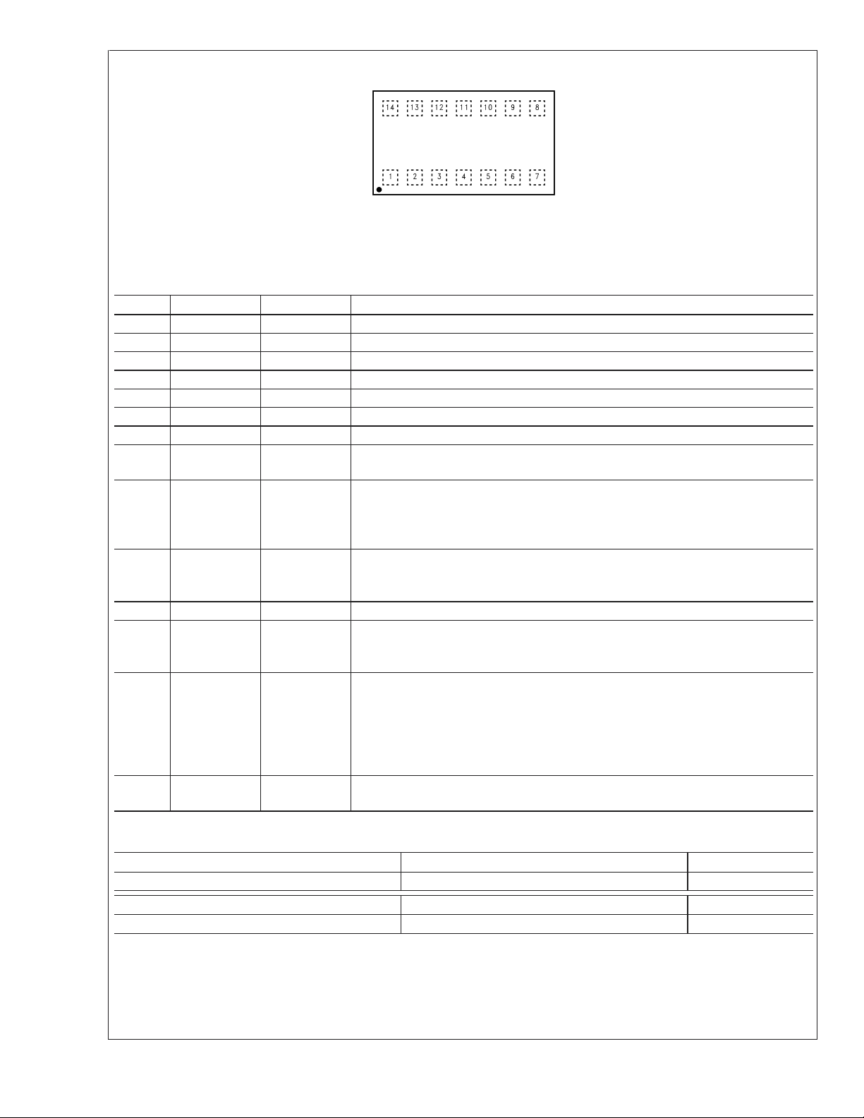
LP3945/LP3946 LLP14 Package Drawing
LP3945/LP3946
(TOP VIEW)
20066503
See NS Package Number LDA14A
LP3945/LP3946 Pin Description
Pin # LP3945 LP3946 Description
1 EN EN Charger Enable Input. Internally pulled high to CHG-IN pin.
2 SCL GND Serial Interface Clock Input for LP3945. Ground in LP3946.
3 SDA GND Serial Interface DATA Input/Output for LP3945. Ground in LP3946.
4 BATT BATT Battery supply input terminal. Must have 10 µF ceramic capacitor to GND.
5V
6VB
BG
SENSE
7 GND GND Digital Ground
8 Diff-Amp Diff-Amp Charge current monitoring differential amplifier output. Voltage output representation
9 BIPB BIPB Battery in Place Bar. Input signal to indicate presence/absence of the battery.
10 EOC EOC Active Low Open Drain Output to drive Green LED. Active when wall adaptor is
11 GND GND Analog Ground
12 CHG CHG Active Low Open Drain Output to drive Red LED. Active when wall adaptor is
13 StopModeEN StopModeEN For normal operation, this pin must be left floating. Pulling this pin to ground will
14 CHG-IN CHG-IN Charger input from a regulated, current limited power source. Must havea1µF
V
VB
BG
SENSE
Bandgap Voltage Reference (1.225V). Factory test point. Must be left floating.
Battery Voltage Sense connected to the + terminal of the battery.
of the charge current.
Internally pulled high to CHG-IN. Pulled low by the Battery ID resistor. Absence of
the ID resistor (BIPB signal high) indicates no battery. Pulling BIPB pin high sets the
device to LDO mode.
connected and battery is fully charged. Regardless of the battery chemistry, this
signal is available whenever a battery is attached.
connected and battery is being charged. Regardless of the battery chemistry, this
signal is available whenever a battery is attached.
bypass the 5.6 Hrs safety timer in constant current mode. See "StopModeEN PIN"
Section for more detail.
WARNING! Disabling the timer is not a recommended operating condition
since it disables the safety timer function. User must provide protection
against continuously charging a defective battery.
ceramic capacitor to GND.
Ordering Information
LP3945 supplied as 1000 units Tape and Reel LP3945 supplied as 4500 units Tape and Reel Package Marking
LP3945ILD LP3945ILDX L00011B
LP3946 supplied as 1000 units Tape and Reel LP3946 supplied as 4500 units Tape and Reel Package Marking
LP3946ILD LP3946ILDX L00030B
The LP3946 has default values of I
Semiconductor Sales Office.
www.national.com 2
=500mA, V
CHG
=4.1V and EOC=0.1C. For other default options, please contact National
BATT
Page 3
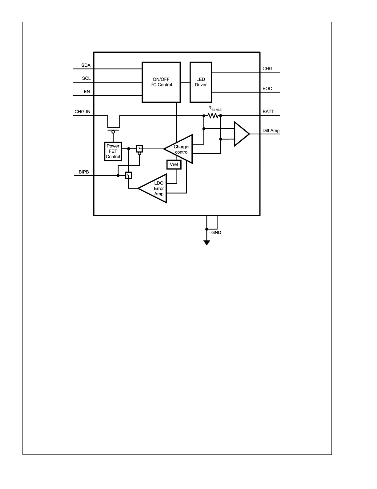
Block Diagram
LP3945/LP3946
LP3945 Functional Block Diagram
20066530
www.national.com3
Page 4
Absolute Maximum Ratings (Notes 1,
2)
If Military/Aerospace specified devices are required,
ESD (Note 4)
Human Body Model
Machine Model
please contact the National Semiconductor Sales Office/
Distributors for availability and specifications.
LP3945/LP3946
CHG-IN −0.3V to +6.5V
BATT, VB
CHG, EN, BIPB, StopModeEN −0.3V to +6V
Junction Temperature 150˚C
Storage Temperature −65˚C to +150˚C
Power Dissipation (Note 3) 1.76W
, SDA, SCL, EOC,
SENSE
Operating Ratings (Notes 1, 2)
CHG-IN 3.0V to 6.0V
EN, BIPB, StopModeEN 0V to (V
Junction Temperature, T
Operating Temperature, T
Thermal Resistance, θ
Maximum Power Dissipation
(TA= 85˚C, (Note 5) ) 1.08W
Electrical Characteristics
Unless otherwise noted, V
mal type apply for T
= −40˚C to +85˚C. (Notes 6, 7, 8)
T
J
= 25˚C. Limits appearing in boldface type apply over the entire junction temperature range for operation,
J
Symbol Parameter Conditions Typical
V
SUPPLY
CC
V
CHG-IN
I
BATT
V
OK−TSHD
V
UVLO−TSHD
V
OVLO−TSHD
Input Voltage Range 4.5 6
Operating Range Battery Connected 4.5 6
Battery Leakage Current
Adapter OK Trip Point (CHG-IN)
Under Voltage Lock-out Trip
Point
Over Voltage Lock-out Trip Point
Thermal Shutdown Temperature
Thermal Shutdown Hysteresis 20 ˚C
BATTERY CHARGER — Li ION MODE (MODE = LOW)
Fast Charge Current Range 500 950 mA
I
CHG
Fast Charge Current Accuracy −10 +10 %
Programmable Charging Current
Step
I
PRE-CHG
I
EOC
Pre-Charge Current V
End Of Charge Current Accuracy For I
Battery Regulation Voltage
(For 4.1V Cell) (Default State)
V
BATT
Battery Regulation Voltage
(For 4.2V Cell)
V
CHG-Q
Full Charge Qualification
Threshold
CHG-IN
= 5V, V
BATT
= 4V, C
V
CHG-IN
= 1µF, C
CHG-IN
≤ 4V 2 20 µA
EOC = Low, adaptor connected,
V
= 4.1V
BATT
V
CHG-IN-VBATT
V
CHG-IN-VBATT
V
V
V
V
(Rising) 4.15 3.8 4.5 V
CHG-IN
(Falling) 3.95 3.6 4.3 V
CHG-IN
(Rising) 5.9
CHG-IN
(Falling) 5.7
CHG-IN
(Note 7)
=2V 50 65 mA
BATT
= 0.1C, 0.15C or 0.2C +20 −20 %
EOC
T
= 0˚C to +85˚C
J
I
CHARGE
T
I
CHARGE
T
I
CHARGE
T
I
CHARGE
V
= 10 mA, Mode = Low
= −40˚C to +85˚C
J
= 10 mA, Mode = Low
= 0˚C to +85˚C
J
= 10 mA, Mode = Low
= −40˚C to +85˚C
J
= 10 mA, Mode = Low
Rising, Transition from
BATT
Pre-Charge to Full Current
= 10µF. Typical values and limits appearing in nor-
BATT
(Rising) 60 mV
(Falling) 50 mV
200V
+0.3V)
CHG-IN
J
A
JA
Min Max
−40˚C to +125˚C
−40˚C to +85˚C
Limit
37˚C/W
Units
50 150 µA
160 ˚C
50 mA
4.1 4.059 4.141
4.1 4.038 4.162
4.2 4.158 4.242
4.2 4.137 4.263
3.0 V
2kV
V
V
V
www.national.com 4
Page 5
Electrical Characteristics (Continued)
Unless otherwise noted, V
mal type apply for T
= −40˚C to +85˚C. (Notes 6, 7, 8)
T
J
= 25˚C. Limits appearing in boldface type apply over the entire junction temperature range for operation,
J
Symbol Parameter Conditions Typical
BATTERY CHARGER — Li ION MODE (MODE = LOW)
Restart Threshold Voltage
V
BAT-RST
(For 4.1V Cell)
Restart Threshold Voltage
(For 4.2V Cell)
Internal Current Sense
R
SENSE
Resistance
Internal Current Sense Resistor
Load Current
ICHG
t
EOC
MON
Diff-Amp Output
Time to EOC State
BATTERY CHARGER — NI-MH MODE (MODE = HIGH, LP3945 ONLY)
V
BATT-MAX
Battery Over Voltage Protection
LDO MODE (BIPB=HIGH)
V
OUT
Output Voltage Regulation
LOGIC LEVELS
V
IL
V
IH
I
IL
Low Level Input Voltage EN 0.4 V
High Level Input Voltage EN 2.0 V
Enable Pin Input Current
CHG-IN
= 5V, V
= 4V, C
BATT
V
BATT
EOC, to Pre-Qualification State
V
BATT
EOC, to Pre-Qualification State
= 1µF, C
CHG-IN
BATT
Falling, Transition from
Falling, Transition from
= 10µF. Typical values and limits appearing in nor-
3.9 3.77 4.02
4.00 3.86 4.12
(Note 7) 120 mΩ
(Note 7) 1.2 A
= 50 mA 0.583
I
CHG
= 500 mA 1.333
CHG
I
= 950 mA 2.090
CHG
0˚C to +85˚C (Note 7) 5.625 4.78 6.42
−40˚C to +85˚C (Note 7) 5.625 4.5 6.75
(Charging Current Decreases to
0 mA when V
Voltage), V
=50mA 4.10
I
LOAD
I
=950mA 4.06
LOAD
BATT
CHG-IN
is above this
= 5.6V
5.4 5.292 5.508 V
EN = LOW −10 +10
EN = HIGH −5 +5
Limit
Min Max
LP3945/LP3946
Units
V
VI
Hrs
V
µA
Electrical Characteristics, I2C Interface (LP3945 Only)
Unless otherwise noted, V
Limits appearing in boldface type apply over the entire junction temperature range for operation, T
6, 7, 8)
Symbol Parameter Conditions Typical
V
V
V
V
F
t
HOLD
IL
IH
OL
HYS
CLK
Low Level Input Voltage SDA & SCL 0.4 0.3 V
High Level Input Voltage SDA & SCL 0.7 V
Low Level Output Voltage SDA & SCL 0 0.2 V
Schmitt Trigger Input Hysteresis SDA & SCL 0.1 V
Clock Frequency 400 kHz
Hold Time Repeated START
Condition
t
CLK-LP
t
CLK-HP
t
SU
CLK Low Period (Note 7) 1.3 µs
CLK High Period (Note 7) 0.6 µs
Set-up Time Repeated START
Condition
t
DATA-HOLD
t
DATA-SU
t
SU
Data Hold Time (Note 7) 300 ns
Data Set-up Time (Note 7) 100 ns
Set-up Time for STOP Condition (Note 7) 0.6 µs
CHG-IN
= 5V, V
= 4V. Typical values and limits appearing in normal type apply for TJ= 25˚C.
BATT
(Note 7)
(Note 7)
= −40˚C to +85˚C. (Notes
J
Limit
Min Max
DDVDD
DD
+0.5 V
Units
DD
DD
0.6 µs
0.6 µs
www.national.com5
V
V
V
Page 6

Electrical Characteristics, I2C Interface (LP3945 Only) (Continued)
Unless otherwise noted, V
Limits appearing in boldface type apply over the entire junction temperature range for operation, T
6, 7, 8)
Symbol Parameter Conditions Typical
LP3945/LP3946
t
TRANS
Maximum Pulse Width of Spikes
that must be Suppressed by the
Input Filter of both DATA & CLK
signals.
Note 1: Absolute Maximum Ratings are limits beyond which damage to the device may occur. Operating Ratings are conditions under which operation of the device
is guaranteed. Operating Ratings do not imply guaranteed performance limits. For guaranteed performance limits and associated test conditions, see the Electrical
Characteristics tables.
Note 2: All voltages are with respect to the potential at the GND pin.
Note 3: The Absolute Maximum power dissipation depends on the ambient temperature and can be calculated using the formula
P=(T
where T
J
Absolute Maximum Ratings results from substituting the Absolute Maximum junction temperature, 150˚C, for T
be dissipated safely at ambient temperature below 85˚C. Less power can be dissipated safely at ambient temperatures above 85˚C. The Absolute Maximum power
dissipation can be increased by 27 mW for each degree below 85˚C, and it must be de-rated by 27 mW for each degree above 85˚C.
Note 4: The human-body model is 100 pF discharged through 1.5 kΩ. The machine model is 0Ω in series with 220pF
Note 5: Like the Absolute Maximum power dissipation, the maximum power dissipation for operation depends on the ambient temperature. The 1.08W rating
appearing under Operating Ratings results from substituting the maximum junction temperature for operation, 125˚C, for T
(1) above. More power can be dissipated at ambient temperatures below 85˚C. Less power can be dissipated at ambient temperatures above 85˚C. The maximum
power dissipation for operation can be increased by 27 mW for each degree below 85˚C, and it must be de-rated by 27 mW for each degree above 85˚C.
Note 6: All limits are guaranteed. All electrical characteristics having room-temperature limits are tested during production with T
guaranteed by correlating the electrical characteristics to process and temperature variations and applying statistical process control.
Note 7: Guaranteed by design.
Note 8: LP3945 and LP3946 are not intended as a Li-Ion battery protection device, battery used in this application should have an adequate internal protection.
)/θJA, (1)
J—TA
is the junction temperature, TAis the ambient temperature, and θJAis the junction-to-ambient thermal resistance. The 1.76W rating appearing under
CHG-IN
= 5V, V
= 4V. Typical values and limits appearing in normal type apply for TJ= 25˚C.
BATT
= −40˚C to +85˚C. (Notes
J
Limit
Min Max
(Note 7)
50 ns
, 85˚C for TA, and 37˚C/W for θJA. More power can
J
, 85˚C for TA, and 37˚C/W for θJAinto
J
= 25˚C. All hot and cold limits are
J
Units
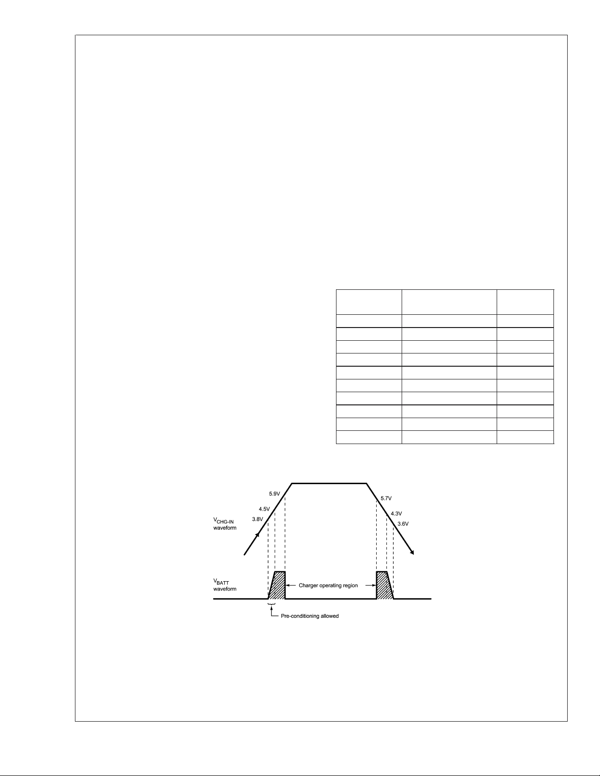
The end of charge current threshold default setting is at 0.1C, this threshold can be set to 0.15 or 0.2 by the controller (see bit chart for detail).
Li-Ion Charging Profile
www.national.com 6
20066504
Page 7

LP3945/LP3946
Typical Performance Characteristics Unless otherwise specified, T
4.1V Termination Voltage vs Temperature 500mA vs Temperature
20066531 20066532
950mA vs Temperature I
CHG
= 25˚C, V
A
vs Diff Amp
CHG-IN
= 5V.
20066533
20066534
www.national.com7
Page 8
Application Notes
LP3945 CHARGER OPERATION
The LP3945 is a complete battery charger with I
Charge cycle is initiated with wall adaptor insertion. If the
LP3945/LP3946
wall adaptor voltage appearing on the CHG-IN pin meets
under-voltage (V
UVLO-TSHD
the Adaptor OK signal is detected, then pre-conditioning
process begins (see Figure 1). In pre-qualification cycle, a
safe current level, less than 65 mA, is pumped into the
battery while the voltage across the battery terminals is
measured. Once this voltage exceeds 3.0V, the controller
will initiate constant current fast charge cycle. During this
cycle, the 5.6 hr safety timer is started and charge current is
increased to I
. The default value for I
CHG
manufacturing to 500 mA but it is user programmable from
500 mA to 950 mA in 50 mA step. The programmed current
is determined by battery type and manufacturers’ recommendation.
If safety timer times out during constant current cycle, charging will be terminated if StopModeEN pin is pulled high. If it
is pulled low, device will proceed to operate in maintenance
mode and have to be interrupted externally. This is not a
recommended mode of operation. Disabling the 5.6hr timer
can potentially expose the battery to prolong charge cycle
and damage the battery. If StopModeEN feature is used,
user must protect the battery from exposure to prolong
charge cycle.
As the battery is charged during constant current mode, the
voltage across pack terminal increases until it reaches 4.1V
(or 4.2V). As soon as pack terminal exceeds 4.1V (or 4.2V),
controller starts operating in constant voltage mode by applying regulated V
BATT
During this cycle, charge current, I
crease with time and when it drops below 0.1C (by default),
the EOC signal is activated indicating successful completion
of the charge cycle. The "C" term in 0.1C is the programmed
. For example, 0.1C of 700mA is 70mA, and 0.2C of
I
CHG
700mA is 140mA. EOC current can be programmed to 0.1C,
0.15C, or 0.2C. The default value is 0.1C. After completing
the full charge cycle, controller will start maintenance cycle
), over-voltage (V
OVLO-TSHD
CHG
voltage across the battery terminal.
, continues to de-
CHG
2
C interface.
), and
is set during
where battery pack voltage is monitored continuously. If
during the maintenance cycle, pack voltage drops below
3.9V, charge cycle will be initiated providing that the wall
adaptor is plugged in and is alive.
Ni-MH charge mode (LP3945 only), which is a constant
voltage mode charging, can be selected by setting the
“mode” bit to HIGH via the I
The LP3945 with I
2
C programming allows maximum flexibil-
2
C interface.
ity in selecting charge current, battery regulation voltage
(4.1V or 4.2V), EOC current and battery type (Li Ion or
Ni-MH). The LP3945 operates in default mode during power
up. See the “I
2
C Interface” section for more detail.
LP3946 CHARGER OPERATION
The LP3946 is a simpler version of the LP3945. It does not
have any I
2
C interface, thus the device operates on default
setting. The values in BOLD in Table 1 are the default
settings. Default settings can be set at the factory to customer’s specifications. For other options, please contact a National Semiconductor sales office.
The LP3946 charges only Li Ion type battery.
TABLE 1. LP3946 Performance Options
Battery Voltage
Regulation (V)
End of Charge Current
Threshold (mA)
Charge
Current (mA)
4.1 0.1C 500
4.2 0.15C 550
0.20C 600
650
700
750
800
850
900
950
FIGURE 1. Charger Power Up and Power Down Waveform
www.national.com 8
20066510
Page 9
Application Notes (Continued)
LP3945/LP3946
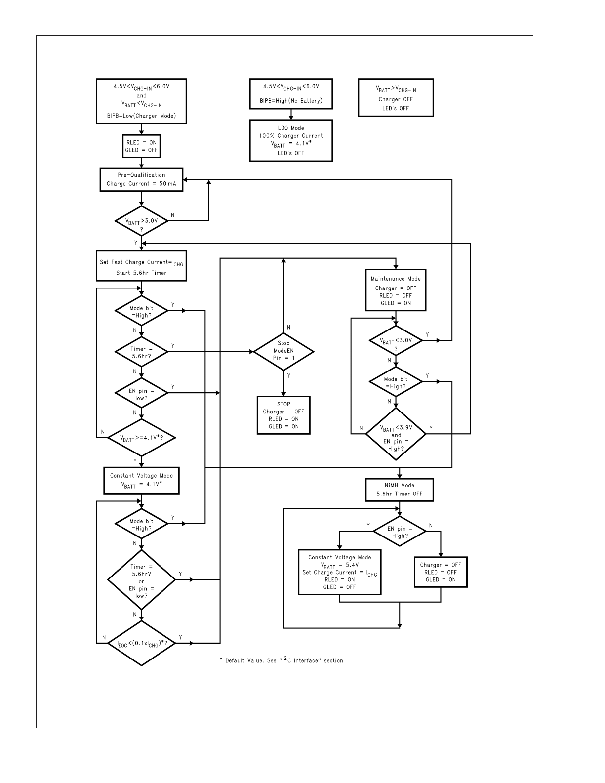
FIGURE 2. LP3945 Charger Flow Chart
20066511
www.national.com9
Page 10
Application Notes (Continued)
LP3945/LP3946
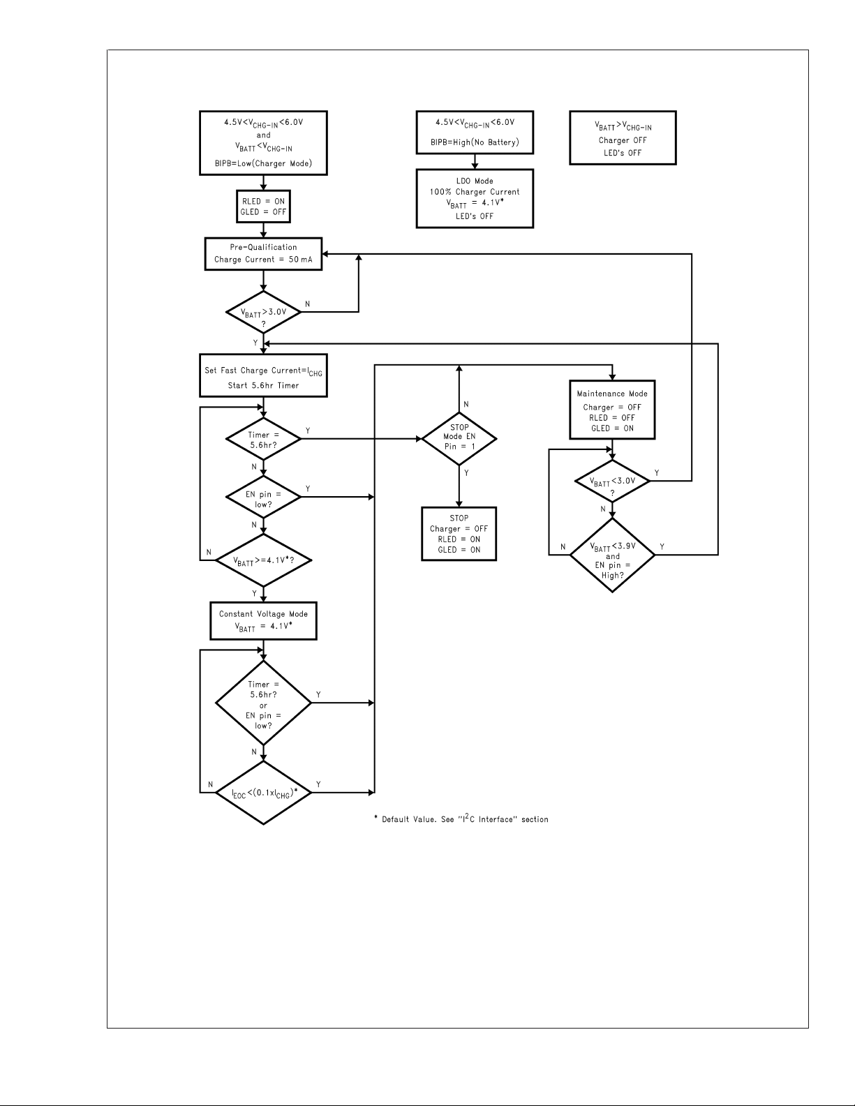
FIGURE 3. LP3946 Charger Flow Chart
www.national.com 10
20066512
Page 11

Application Notes (Continued)
CHARGE CURRENT SELECTION
The LP3945 and LP3946 are designed to provide a charge
current ranging from 500 mA to 950 mA, in 50 mA resolution,
to support batteries with different capacity ratings. No external resistor is required to set the charge current in the
LP3945 and LP3946. This entirely eliminates design time,
external component board space and stability issue.
The LP3945 uses the I
current while the LP3946 has a pre-programmed charge
current.
BATTERY VOLTAGE SELECTION
The battery voltage regulation is set to 4.1V during the
manufacturing. The 4.2V option can be selected on LP3945
via the I
2
C interface or set at the factory for LP3946.
The Ni-MH charge mode is only available in LP3945.
END OF CHARGE (EOC) CURRENT SELECTION
The EOC thresholds can be programmed to 0.1C, 0.15C and
0.2C in the LP3945. The default value is 0.1C, which provides the highest energy storage, but at the expense of
longer charging time. On the other hand, 0.2C takes the
least amount of charging time, but yields the least energy
2
C interface to program the charge
storage. The LP3946 has 0.1C as pre-programmed EOC
threshold. 0.15C and 0.2C options are available upon request.
No EOC function is available during Ni-MH charge cycle.
User must provide a reliable method for charge termination.
CHARGE CURRENT SENSE DIFFERENTIAL AMPLIFIER
The charge current is monitored across the internal 120 mΩ
current sense resistor. The differential amplifier provides the
analog representation of the charge current. Charge current
can be calculated using the following equation:
Where voltage at Diff Amp output (V
charge current (I
) is in amps.
CHG
) is in volt, and
DIFF
Monitoring the Diff Amp output during constant voltage cycle
can provide an accurate indication of the battery charge
status and the time remaining to EOC. This feature is particularly useful during Ni-MH charge cycle. The current
sense circuit is operational in the LDO mode as well. It can
be used to monitor the system current consumption during
testing.
LP3945/LP3946
FIGURE 4. Charge Current Monitoring Circuit (Diff-Amp)
LED CHARGE STATUS INDICATORS
The LP3945 and LP3946 are equipped with two open drain
outputs to drive a green LED and a red LED. These two
LEDs work together in combinations to indicate charge status or fault conditions. Table 2 shows all the conditions.
20066514
TABLE 2. LED Indicator Summary
Charger Status RED
LED
GREEN
LED
Charger Off OFF OFF
Charging Li Ion Battery* ON OFF
Maintenance Mode OFF ON
Charging Li Ion Battery after
OFF ON
Passing Maintenance Mode
Charging Ni-MH in Constant
ON OFF
Voltage Mode
EN Pin = LOW OFF ON
LDO Mode OFF OFF
5.6 Hr Safety Timer Flag ON ON
*Charging Li Ion battery for the first time after V
CHG-IN
insertion.
www.national.com11
Page 12
Application Notes (Continued)
BIPB PIN
BIPB pin is used to select between charger mode and LDO
mode. It is pulled HIGH internally to the CHG-IN pin, which is
the LDO mode. To select charger mode, this pin must be
LP3945/LP3946
connected to ground directly or pulled to ground via the
battery pack ID resistor. In the latter case, BIPB pin pulled
LOW confirms battery connection. Alternatively, this pin can
be pulled to LOW by the system micro-controller for added
flexibility.
LDO MODE
The charger is in the LDO mode when the BIPB pin is left
open or HIGH. This mode of operation is used primarily
during system level testing of the handset to eliminate the
need for battery insertion. CAUTION: battery may be damaged if device is operating in LDO mode with battery connected.
The internal power FET provides up to 1.2 amp of current at
BATT pin in this mode. The LDO output is set to 4.1V. When
operating at higher output currents, care must be taken not
to exceed the package power dissipation rating. See “Thermal Performance of LLP Package” section for more detail.
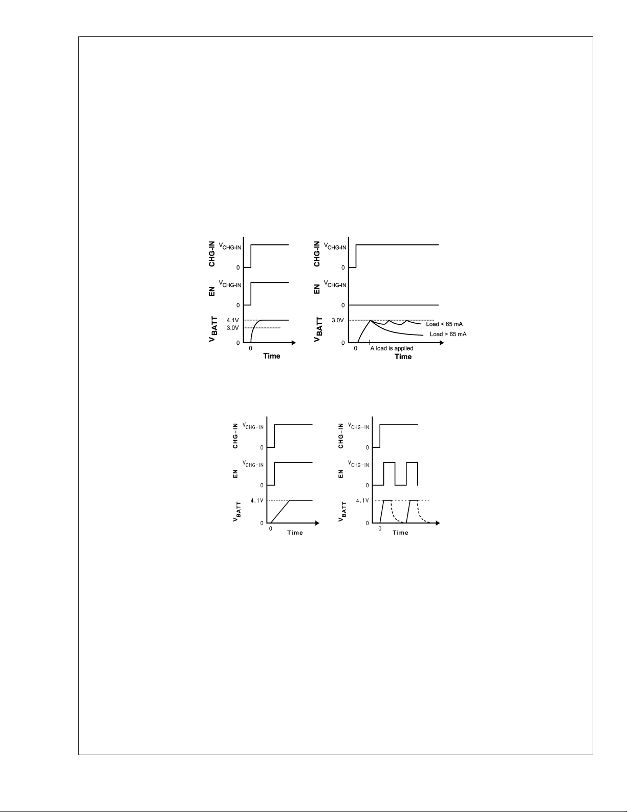
EN PIN
The Enable pin is used to enable/disable the charger, in both
charger mode and LDO mode, see Figure 5 and Figure 6.
The Enable pin is internally pulled HIGH to the CHG-IN pin.
When the charger is disabled, it draws less than 4 µA of
current.
FIGURE 5. Power Up Timing Diagram in Charger Mode (BIPB = LOW)
FIGURE 6. Power Up Timing Diagram in LDO Mode (BIPB = HIGH)
5.6 HR SAFETY TIMER IN CHARGER MODE
Both LP3945 and LP3946 have built-in 5.6 hr back up safety
timer to prevent over-charging a Li Ion battery. The 5.6 hr
timer starts counting when the charger enters constant current mode. It will turn the charger off when the 5.6 hr timer is
up while the charger is still in constant current mode. In this
case, both LEDs will turn on, indicating a fault condition.
In order for the 5.6 hr safety timer to function in the LP3945,
pin 13 should be left floating. CAUTION: disabling the back
up safety timer could create unsafe charging conditions. If
disabled, user must provide external protection to prevent
overcharging the battery.
20066515
20066516
StopModeEN PIN
To provide the flexibility of using an external back up timer,
StopModeEN allows “bypassing” of the 5.6 hr safety timer. It
is achieved by pulling pin 13 on the LP3945 to LOW. As
indicated in the LP3945 Flow Chart, this feature works only
in constant current mode with a Li Ion battery. Therefore, if a
Li Ion battery is in constant current mode and the 5.6 hr timer
times out, instead of the charger being turned off, it proceeds
to maintenance mode.
This is not a recommended mode of operation. Disabling the
5.6 hr timer can potentially expose the battery to prolong
charge cycle and damage the battery. If StopModeEn feature
is used, user must protect the battery from exposure to
prolong charge cycle. For normal operation, pin 13 should be
left floating.
www.national.com 12
Page 13

2
C INTERFACE (LP3945 ONLY)
Application Notes (Continued)
NI-MH MODE (LP3945 ONLY)
Programming the “mode” bit to HIGH sets the LP3945 to
Ni-MH mode and charges the battery in constant voltage
mode until the battery voltage reaches 5.4V. Since each cell
of the Ni-MH is 1.25V when fully charged, the LP3945 can
only charge exactly four cells. Charging is terminated by the
system micro-controller timer by monitoring the charge cur-
I
2
C interface is used in the LP3945 to program various
I
parameters as shown in Table 3. The LP3945 operates on
default settings during power up. Once programmed, the
LP3945 retains the register data as long as the battery
voltage is above 2.85V. Table 4 shows the charge current
and EOC current programming code.
2
Figures 7, 8 display I
C read/write format.
rent. The system micro-controller reads the charge current
value from the Diff Amp output. Charge current in Ni MH can
be programed as in Li Ion mode, from 950 mA to 500 mA in
50 mA step. The 5.6 hr timer is disabled in Ni-MH mode.
TABLE 3. LP3945 Serial Port Communication Address Code 7h'45
LP3945 Control and Data Codes
Addrs Register 7 6 5 4 3 2 1 0
8'h00 Charger
Register −1
8'h01 Charger
Register −2
Numbers in parentheses indicate default setting. “0” bit is set to low state, and “1” bit is set to high state. R/O — Read Only. All other bits are Read and Write.
Mode
(0) = Li-Ion
1 = Ni-MH
Batt Voltage
(0) = 4.1V
1 = 4.2V
EOC
(Green LED)
R/O
Charger
Current
Code 3
(0)
Charging
(Red LED)
R/O
Charger
Current
Code 2
(0)
EOC Sel −1
(0)
Charger
Current
Code 1
(0)
EOC Sel −0
(1)
Charger
Current
Code 0
(0)
LP3945/LP3946
TABLE 4. Charger Current and EOC Current Programming Code
Data Code
Charger Current Selection
SET
(mA)
Code I
Data Code
End of Charge Current
Selection Code
4h'00 500
4h'01 550 2h’1 0.1C
4h'02 600 2h’2 0.15C
4h'03 650 2h’3 0.2C
4h'04 700
4h'05 750
4h'06 800
4h'07 850
4h'08 900
4h'09 950
w = write (sda = “0”)
r = read (sda = “1”)
ack = acknowledge (sda pulled down by either master or slave)
rs = repeated start
FIGURE 7. LP3945 (Slave) Register Write
20066517
www.national.com13
Page 14

Application Notes (Continued)
LP3945/LP3946
w = write (sda = “0”)
r = read (sda = “1”)
ack = acknowledge (sda pulled down by either master or slave)
rs = repeated start
FIGURE 8. LP3945 (Slave) Register Read
THERMAL PERFORMANCE OF LLP PACKAGE
The LP3945 and LP3946 are monolithic devices with integrated pass transistors. To enhance the power dissipation
performance, the Leadless Lead frame Package, or LLP, is
used. The LLP package is designed for improved thermal
performance because of the exposed die attach pad at the
bottom center of the package. It brings advantage to thermal
performance by creating a very direct path for thermal dissipation. Compared to the traditional leaded packages where
the die attach pad is embedded inside the mold compound,
the LLP reduces a layer of thermal path.
The thermal advantage of the LLP package is fully realized
only when the exposed die attach pad is soldered down to a
thermal land on the PCB board and thermal vias are planted
underneath the thermal land. Based on a LLP thermal measurement, junction to ambient thermal resistance (θ
JA
) can
be improved by as much as two times if a LLP is soldered on
the board with thermal land and thermal vias than if not.
An example of how to calculate for LLP thermal performance
is shown below:
20066518
power dissipation for operation can be increased by 27 mW
for each degree below 70˚C, and it must be de-rated by 27
mW for each degree above 70˚C.
LAYOUT CONSIDERATION
The LP3945 and LP3946 have exposed die attach pad
located at the bottom center of the LLP package. It is imperative to create a thermal land on the PCB board when
designing a PCB layout for the LLP package. The thermal
land helps to conduct heat away from the die, and the land
should be the same dimension as the exposed pad on the
bottom of the LLP (1:1 ratio). In addition, thermal vias should
be added inside the thermal land to conduct more heat away
from the surface of the PCB to the ground plane. Typical
pitch and outer diameter for these thermal vias are 1.27 mm
and 0.33 mm respectively. Typical copper via barrel plating is
1 oz. although thicker copper may be used to improve thermal performance. The LP3945 and LP3946 bottom pad is
connected to ground. Therefore, the thermal land and vias
on the PCB board need to be connected to ground.
For more information on board layout techniques, refer to
Application Note 1187 “Leadless Leadframe Package
(LLP)”. The application note also discuss package handling,
solder stencil, and assembly.
By substituting 37˚C/W for θJA, 125˚C for TJand 70˚C for TA,
the maximum power dissipation allowed from the chip is
1.48W at T
= 70˚C. If V
A
is being charged, then 740 mA of I
is at 5.0V and a 3.0V battery
CHG-IN
can safely charge the
CHG
battery. More power can be safely dissipated at ambient
temperatures below 70˚C. Less power can be safely dissipated at ambient temperatures above 70˚C. The maximum
www.national.com 14
LP3945 AND LP3946 EVALUATION BOARDS
The LP3945 and LP3946 evaluation boards and instruction
manuals are available for order on National’s website
(www.national.com). The LP3945 evaluation board has on-
2
C interface capability for more flexibility. Please visit
board I
National’s website for more detail.
Page 15

Physical Dimensions inches (millimeters) unless otherwise noted
LP3945/LP3946 Battery Charge Management System
NS Package Number LDA14A
LIFE SUPPORT POLICY
NATIONAL’S PRODUCTS ARE NOT AUTHORIZED FOR USE AS CRITICAL COMPONENTS IN LIFE SUPPORT
DEVICES OR SYSTEMS WITHOUT THE EXPRESS WRITTEN APPROVAL OF THE PRESIDENT AND GENERAL
COUNSEL OF NATIONAL SEMICONDUCTOR CORPORATION. As used herein:
1. Life support devices or systems are devices or
systems which, (a) are intended for surgical implant
into the body, or (b) support or sustain life, and
whose failure to perform when properly used in
accordance with instructions for use provided in the
2. A critical component is any component of a life
support device or system whose failure to perform
can be reasonably expected to cause the failure of
the life support device or system, or to affect its
safety or effectiveness.
labeling, can be reasonably expected to result in a
significant injury to the user.
National Semiconductor
Americas Customer
Support Center
Email: new.feedback@nsc.com
Tel: 1-800-272-9959
www.national.com
National Semiconductor
Europe Customer Support Center
Fax: +49 (0) 180-530 85 86
Email: europe.support@nsc.com
Deutsch Tel: +49 (0) 69 9508 6208
English Tel: +44 (0) 870 24 0 2171
Français Tel: +33 (0) 1 41 91 8790
National Semiconductor
Asia Pacific Customer
Support Center
Email: ap.support@nsc.com
National Semiconductor
Japan Customer Support Center
Fax: 81-3-5639-7507
Email: jpn.feedback@nsc.com
Tel: 81-3-5639-7560
National does not assume any responsibility for use of any circuitry described, no circuit patent licenses are implied and National reserves the right at any time without notice to change said circuitry and specifications.
 Loading...