


LP3944
RGB/White/Blue 8-LED Fun Light Driver
LP3944 RGB/White/Blue 8-LED Fun Light Driver
November 2003
General Description
LP3944 is an integrated device capable of independently
driving 8 LEDs. This device also contains an internal precision oscillator that provides all the necessary timing required
for driving each LED. Two prescaler registers along with two
PWM registers provide a versatile duty cycle control. The
LP3944 contains the ability to dim LEDs in SMBUS/I
applications where it is required to cut down on bus traffic.
Traditionally, to dim LEDs using a serial shift register such as
74LS594/5 would require a large amount of traffic to be on
the serial bus. LP3944 instead requires only the setup of the
frequency and duty cycle for each output pin. From then on,
only a single command from the host is required to turn each
individual open drain output ON, OFF, or to cycle a programmed frequency and duty cycle. Maximum output sink
current is 25 mA per pin and 200 mA per package. Any ports
not used for controlling the LEDs can be used for general
purpose input/output expansion.
2
Typical Application Circuit
Features
n Internal power-on reset
n Active low reset
n Internal precision oscillator
n Variable dim rates (from 6.25 ms to 1.6s;
160 Hz– 0.625 Hz)
C
Key Specifications
n 8 LED driver (multiple programmable states — on, off,
input, and dimming at a specified rate)
n 8 Open drain outputs capable of driving up to 25 mA per
LED
Applications
n Customized flashing LED lights for cellular phones
n Portable Applications
n Digital Cameras
n Indicator Lamps
n General purpose I/O expander
n Toys
20085301
© 2003 National Semiconductor Corporation DS200853 www.national.com
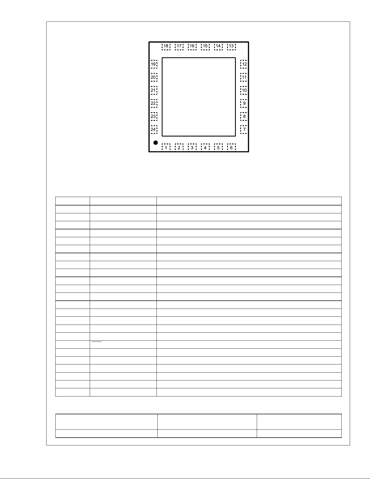
LP3944 Pin Out
LP3944
(Top View)
See NS Package Number SQA24A
LP3944 Pin Description
Pin # Name Description
1 LED0 Output of LED0 Driver
2 LED1 Output of LED1 Driver
3 LED2 Output of LED2 Driver
4 LED3 Output of LED3 Driver
5 LED4 Output of LED4 Driver
6 LED5 Output of LED5 Driver
7 LED6 Output of LED6 Driver
8 LED7 Output of LED7 Driver
9 GND Ground
10 NC No Connect
11 NC No Connect
12 NC No Connect
13 NC No Connect
14 NC No Connect
15 NC No Connect
16 NC No Connect
17 NC No Connect
18 RST
19 SCL Clock Line for I
20 SDA Serial Data Line for I
21 V
22 A0 Address Input 0
23 A1 Address Input 1
24 A2 Address Input 2
DD
Active Low Reset Input
Power Supply
2
C Interface
2
C Interface
20085302
Ordering Information
LP3944, Supplied as 1000 Units, Tape and
Reel
LP3944ISQ LP3944ISQX
www.national.com 2
LP3944, Supplied as 4500 Units, Tape
and Reel
Package Marking
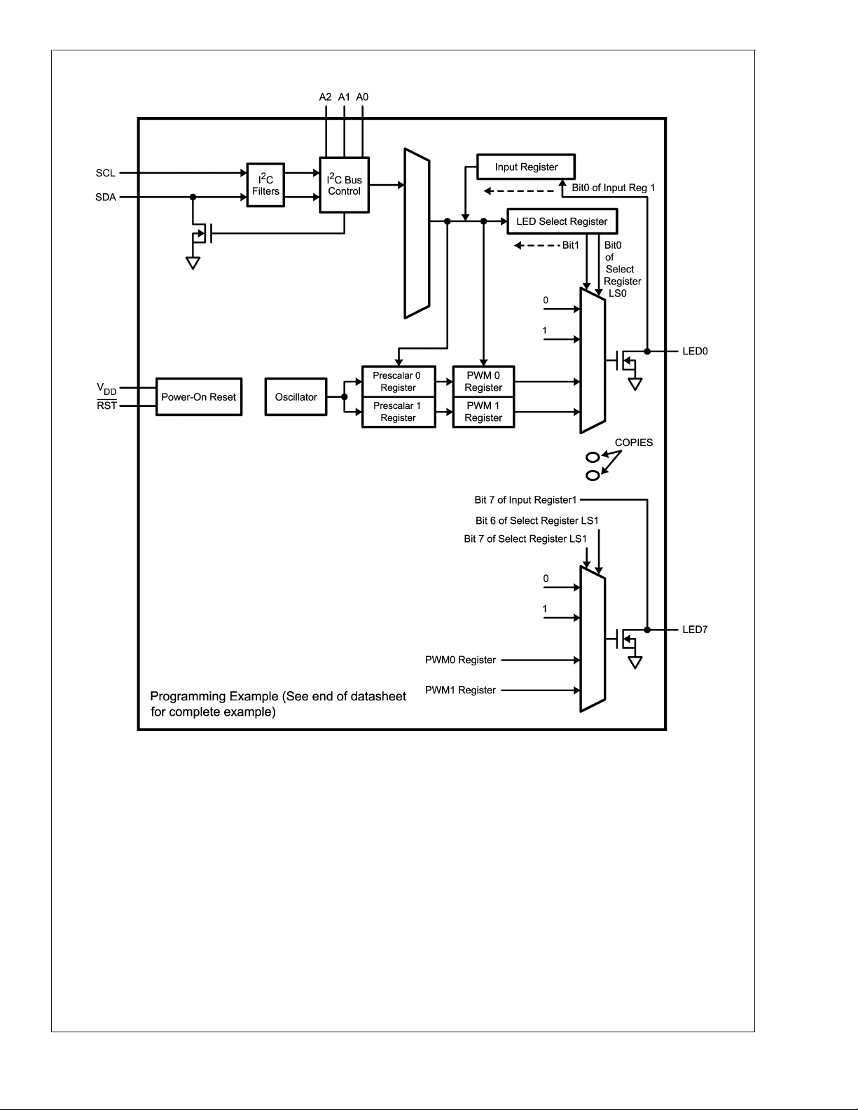
Architectural Block Diagram
LP3944
For Explanation of LP3944 Operation, Please Refer to “Theory of Operation” in Application Notes.
20085303
www.national.com3
Absolute Maximum Ratings (Notes 2,
1)
LP3944
If Military/Aerospace specified devices are required,
Human Body Model 2 kV
Machine Model 150V
Charge Device Model 1 kV
please contact the National Semiconductor Sales Office/
Distributors for availability and specifications.
V
DD
−0.5V to 6V
A0, A1, A2, SCL, SDA, RST
(Collectively called digital pins)
Voltage on LED pins V
−0.5V to 6V
SS
Junction Temperature 150˚C
Storage Temperature −65˚C to 150˚C
Power Dissipation (Note 3) 1.76W
6V
Operating Ratings (Notes 1, 2)
V
DD
Junction Temperature −40˚C to +125˚C
Operating Ambient Temperature −40˚C to +85˚C
Thermal Resistance (θ
LLP24 (Note 3) 37˚C/W
Power Dissipation 1.08W
)
JA
ESD (Note 4)
Electrical Characteristics
Unless otherwise noted, VDD= 5.5V. Typical values and limits appearing in normal type apply for TJ= 25˚C. Limits appearing
in boldface type apply over the entire junction temperature range for operation, T
Symbol Parameter Conditions Typical
POWER SUPPLY
V
DD
I
Q
Supply Voltage 5 2.3 5.5 V
Supply Current No Load 350 550
Standby 2.0 5
∆I
Q
Additional Standby Current VDD= 5.5V, every LED pin
at 4.3V
V
POR
t
w
Power-On Reset Voltage 1.8 1.96 V
Reset Pulse Width 10 ns
LED
V
IL
V
IH
I
OL
LOW Level Input Voltage −0.5 0.8 V
HIGH Level Input Voltage 2.0 5.5 V
Low Level Output Current
VOL= 0.4V, VDD= 2.3V
(Note 6)
VOL= 0.4V, VDD= 3.0V 12
V
= 0.4V, VDD= 5.0V 15
OL
V
= 0.7V, VDD= 2.3V 15
OL
V
= 0.7V, VDD= 3.0V 20
OL
V
= 0.7V, VDD= 5.0V 25
OL
I
LEAK
C
I/O
Input Leakage Current VDD= 3.6, VIN=0VorV
DD
Input/Output Capacitance (Note 7) 2.6 5 pF
ALL DIGITAL PINS (EXCEPT SCL AND SDA PINS)
V
IL
V
IH
I
LEAK
C
IN
2
I
C INTERFACE (SCL AND SDA PINS)
V
IL
V
IH
V
OL
I
OL
F
CLK
t
HOLD
LOW Level Input Voltage −0.5 0.8 V
HIGH Level Input Voltage 2.0 5.5 V
Input Leakage Current −1 1 µA
Input Capacitance VIN= 0V (Note 7) 2.3 5 pF
LOW Level Input Voltage -0.5 0.3V
HIGH Level Input Voltage 0.7V
LOW Level Output Voltage 0 0.2V
LOW Level Output Current VOL= 0.4V 6.5 3 mA
Clock Frequency (Note 7) 400 kHz
Hold Time Repeated START
(Note 7)
Condition
= −40˚C to +125˚C. (Note 5)
J
Limit
Min Max
9
−1 1 µA
DD
0.6 µs
2 mA
DD
5.5 V
DD
2.3V to 5.5V
Units
µA
mA
V
V
www.national.com 4

Electrical Characteristics (Continued)
Unless otherwise noted, VDD= 5.5V. Typical values and limits appearing in normal type apply for TJ= 25˚C. Limits appearing
in boldface type apply over the entire junction temperature range for operation, T
Symbol Parameter Conditions Typical
2
I
C INTERFACE (SCL AND SDA PINS)
t
CLK-LP
t
CLK-HP
t
SU
CLK Low Period (Note 7) 1.3 µs
CLK High Period (Note 7) 0.6 µs
Set-Up Time Repeated
(Note 7)
START Condition
t
DATA-HOLD
t
DATA-SU
t
SU
Data Hold Time (Note 7) 300 ns
Data Set-Up Time (Note 7) 100 ns
Set-Up Time for STOP
(Note 7)
Condition
t
TRANS
Maximum Pulse Width of
(Note 7)
Spikes that Must Be
Suppressed by the Input
Filter of Both DATA & CLK
Signals
Note 1: Absolute Maximum Ratings are limits beyond which damage to the device may occur. Operating Ratings are conditions under which operation of the device
is guaranteed. Operating Ratings do not imply guaranteed performance limits. For guaranteed performance limits and associated test conditions, see the Electrical
Characteristics tables.
Note 2: All voltages are with respect to the potential at the GND pin.
Note 3: The Absolute Maximum power dissipation depends on the ambient temperature and can be calculated using the formula
P=(T
where T
J
Absolute Maximum Ratings results from substituting the Absolute Maximum junction temperature, 150˚C, for T
be dissipated safely at ambient temperature below 85˚C. Less power can be dissipated safely at ambient temperatures above 85˚C. The Absolute Maximum power
dissipation can be increased by 27 mW for each degree below 85˚C, and it must be de-rated by 27 mW for each degree above 85˚C. For Operating Ratings
maximum power dissipation, T
Note 4: The human-body model is 100 pF discharged through 1.5 kΩ. The machine model is 0Ω in series with 220 pF.
Note 5: Limits are guaranteed. All electrical characteristics having room-temperature limits are tested during production with T
guaranteed by correlating the electrical characteristics to process and temperature variations and applying statistical process control.
Note 6: Each LED pin should not exceed 25 mA and the package should not exceed a total of 200 mA.
Note 7: Guaranteed by design.
)/θJA, (1)
J—TA
is the junction temperature, TAis the ambient temperature, and θJAis the junction-to-ambient thermal resistance. The 1.76W rating appearing under
= 125˚C and TA= 85˚C
J
= −40˚C to +125˚C. (Note 5)
J
Limit
Min Max
Units
0.6 µs
0.6 µs
50 ns
, 85˚C for TA, and 37˚C/W for θJA. More power can
J
= 25˚C. All hot and cold limits are
J
LP3944
Typical Performance Characteristics
Frequency vs. Temp
= −40˚C to +85˚C),
(T
A
= 2.3V to 3.0V
V
DD
20085317
www.national.com5

Application Notes
LP3944
THEORY OF OPERATION
The LP3944 takes incoming data and feed them into several
registers that control the frequency and the duty cycle of the
LEDs. Two prescaler registers and two PWM registers provide two individual rates to dim or blink the LEDs (for more
information on these registers, refer to Table 1. LP3944
REGISTER TABLE). The baseband controller/
microprocessor can program each LED to be in one of four
states —on, off, DIM0 rate or DIM1 rate. One read-only
registers provide status on all 8 LEDs. The LP3944 can be
used to drive RGB LEDs and/or single-color LEDs to create
a colorful, entertaining, and informative setting. This is particularly suitable for accessory functions in cellular phones
and toys. Any LED pins not used to drive LED can be used
for General Purpose Parallel Input/Output (GPIO) expansion.
The LP3944 is equipped with Power-On Reset that holds the
chip in a reset state until V
Once V
is achieved, the LP3944 comes out of reset and
POR
reaches V
DD
during power up.
POR
initializes itself to the default state.
To bring the LP3944 into reset, hold the RST pin LOW for a
period of TW. This will put the chip to its default state. The
LP3944 can only be programmed after RST signal is HIGH
again.
2
I
C DATA VALIDITY
The data on SDA line must be stable during the HIGH period
of the clock signal (SCL). In other words, state of the data
line can only be changed when CLK is LOW.
20085306
FIGURE 1. I2C Data Validity
2
C START AND STOP CONDITIONS
I
START and STOP bits classify the beginning and the end of
2
C session. START condition is defined as SDA signal
the I
transitioning from HIGH to LOW while SCL line is HIGH.
STOP condition is defined as the SDA transitioning from
LOW to HIGH while SCL is HIGH. The I
2
C master always
FIGURE 2. I2C START and STOP Conditions
TRANSFERRING DATA
Every byte put on the SDA line must be eight bits long with
the most significant bit (MSB) being transferred first. The
number of bytes that can be transmitted per transfer is
unrestricted. Each byte of data has to be followed by an
acknowledge bit. The acknowledge related clock pulse is
generated by the master. The transmitter releases the SDA
line (HIGH) during the acknowledge clock pulse. The receiver must pull down the SDA line during the 9th clock
pulse, signifying an acknowledge.A receiver which has been
addressed must generate an acknowledge after each byte
has been received.
2
generates START and STOP bits. The I
to be busy after START condition and free after STOP condition. During data transmission, I
C bus is considered
2
C master can generate
repeated START conditions. First START and repeated
START conditions are equivalent, function-wise.
20085307
After the START condition, a chip address is sent by the I
2
master. This address is seven bits long followed by an eighth
bit which is a data direction bit (R/W). The LP3944 hardwires
bits 7 to 4 and leaves bits 3 to 1 selectable, as shown in
Figure 3. For the eighth bit, a “0” indicates a WRITE and a
“1” indicates a READ. The LP3944 supports only a WRITE
during chip addressing. The second byte selects the register
to which the data will be written. The third byte contains data
to write to the selected register.
C
www.national.com 6

Application Notes (Continued)
LP3944
20085308
FIGURE 3. Chip Address Byte
w = write (SDA = “0”)
r = read (SDA = “1”)
ack = acknowledge (SDA pulled down by either master or slave)
rs = repeated start
xx=60to67
FIGURE 4. LP3944 Register Write
However, if a READ function is to be accomplished, a
WRITE function must precede the READ function, as shown
in Figure 5.
w = write (SDA = “0”)
r = read (SDA = “1”)
ack = acknowledge (SDA pulled down by either master or slave)
rs = repeated start
xx=60to67
20085309
20085310
FIGURE 5. LP3944 Register Read
www.national.com7

Application Notes (Continued)
LP3944
AUTO INCREMENT
Auto increment is a special feature supported by the LP3944
to eliminate repeated chip and register addressing when
data are to be written to or read from registers in sequential
order. The auto increment bit is inside the register address
byte, as shown in Figure 6. Auto increment is enabled when
this bit is programmed to “1” and disabled when it is programmed to “0”.
20085311
FIGURE 6. Register Address Byte
In the READ mode, when auto increment is enabled, I
2
master could receive any number of bytes from LP3944
without selecting chip address and register address again.
Every time the I
increment the register address and the next data register will
be read. When I
2
C master reads a register, the LP3944 will
2
C master reaches the last register (09H
register), the register address will roll over to 00H.
In the WRITE mode, when auto increment is enabled, the
LP3944 will increment the register address every time I
2
master writes to register. When the last register (09H register) is reached, the register address will roll over to 02H,
FIGURE 7. Programming with Auto Increment Disabled (in WRITE Mode)
C
because the first two registers in LP3944 are read-only
registers. It is possible to write to these two registers, and the
LP3944 will acknowledge, but the data will be ignored.
In the LP3944, registers 0x01, 0x08 and 0x09 are not functional. However, it is still necessary to read from 0x01 and to
write to 0x08 and 0x09 in Auto Increment mode. They cannot
be skipped.
2
C
If auto increment is disabled, and the I
change register address, it will continue to write data into the
C master does not
same register.
20085312
FIGURE 8. Programming with Auto Increment Enabled (in WRITE Mode)
www.national.com 8
20085313

Application Notes (Continued)
TABLE 1. LP3944 REGISTER TABLE
Address (Hex) Register Name Read/Write Register Function
0x00 Input 1 Read Only LED0–7 Input Register
0x01 Register 1 Read Only None
0x02 PSC0 R/W Frequency Prescaler 0
0x03 PWM0 R/W PWM Register 0
0x04 PSC1 R/W Frequency Prescaler 1
0x05 PWM1 R/W PWM Register 1
0x06 LS0 R/W LED0–3 Selector
0x07 LS1 R/W LED4–7 Selector
0x08 Register 8 R/W None
0x09 Register 9 R/W None
Note: Registers 1, 8 and 9 are empty and non-functional registers. Register 1 is read-only, with all bits hard-wired to zero. Registers 8 and 9 can be written and read,
but the content does ot have any effect on the operation of the LP3944.
BINARY FOMAT FOR INPUT REGISTERS (READ ONLY)— ADDRESS 0x00 and 0x01
Address 0x00
Bit# 76543210
Default value XXXXXXXX
LED7 LED6 LED5 LED4 LED3 LED2 LED1 LED0
X = don’t care
LP3944
BINARY FORMAT FOR FREQUENCY PRESCALER AND PWM REGISTERS — ADDRESS 0x02 to 0x05
Address 0x02 (PSC0)
Bit# 76543210
Default value 00000000
PSC0 register is used to program the period of DIM0.
DIM0 = (PSC0+1)/160
The maximum period is 1.6s when PSC0 = 255.
Address 0x03 (PWM0)
Bit# 76543210
Default value 10000000
PWM0 register determines the duty cycle of DIM0. The LED outputs are LOW (LED on) when the count is less than the value in PWM0 and HIGH (LED off) when
it is greater. If PWM0 is programmed with 0x00, LED output is always HIGH (LED off).
The duty cycle of DIM0 is: PWM0/256
Default value is 50% duty cycle.
Address 0x04 (PSC1)
Bit# 76543210
Default value 00000000
PSC1 register is used to program the period of DIM1.
DIM1 = (PSC1 + 1)/160
The maximum period is 1.6s when PSC1 = 255.
www.national.com9

Application Notes (Continued)
LP3944
Bit# 76543210
Default value 10000000
PWM1 register determines the duty cycle of DIM1. The LED outputs are LOW (LED on) when the count is less than the value in PWM1 and HIGH (LED off) when
it is greater. If PWM1 is programmed with 0x00, LED output is always HIGH (LED off).
The duty cycle of DIM1 is: PWM1/256
Default value is 50% duty cycle.
BINARY FORMAT FOR SELECTOR REGISTERS — ADDRESS 0x06 to 0x07
Bit# 76543210
Default value 00000000
B1 B0 B1 B0 B1 B0 B1 B0
LED3 LED2 LED1 LED0
Bit# 76543210
Default value 00000000
B1 B0 B1 B0 B1 B0 B1 B0
LED7 LED6 LED5 LED4
Address 0x05 (PWM1)
Address 0x06 (LS0)
Address 0x07 (LS1)
LED States With Respect To Values in "B1" and "B0"
B1 B0 Function
0 0 Output Hi-Z
(LED off)
0 1 Output LOW
(LED on)
1 0 Output dims
(DIM0 rate)
1 1 Output dims
(DIM1 rate)
Programming Example:
Dim LEDs 0 to 7 at 1 Hz at 25% duty cycle
Step 1: Set PSC0 to achieve DIM0 of 1s
Step 2: Set PWM0 duty cycle to 25%
Step 3: Set PSC1 to achieve DIM1 of 0.2s
Step 4: Set LEDs 0 to 7 to point to DIM0
Step Description Register Name Set to (Hex)
1 Set DIM0 = 1s
PSC0 0x09F
1 = (PSC0 + 1)/160
PSC0 = 159
2 Set duty cycle to 25%
PWM0 0x40
Duty Cycle = PWM0/256
PWM0 = 64
3 Set DIM1 = 0.2s
PSC1 0x1F
0.2 = (PSC1 + 1)/160
PSC1 = 31
4 LEDs0to7
LS0, LS1 LS0 = 0xAA
Output = DIM0
LS1 = 0xAA
www.national.com 10

Application Notes (Continued)
REDUCING I
In many applications, the LEDs and the LP3944 share the
same V
When the LEDs are off, the LED pins are at a lower potential
WHEN LEDS ARE OFF
Q
, as shown in Section Typical Application Circuit.
DD
FIGURE 9. Methods to Reduce IQWhen LEDs Are Off
Application Circuit
than V
, causing extra supply current (∆IQ). To minimize
DD
this current, consider keeping the LED pins at a voltage
equal to or greater than V
.
DD
20085314
LP3944
20085315
www.national.com11

Physical Dimensions inches (millimeters) unless otherwise noted
NOTES: UNLESS OTHERWISE SPECIFIED
1. FOR LEAD FINISH THICKNESS AND COMPOSITION. SEE “SOLDER INFORMATION” IN THE PACKAGING SECTION
LP3944 RGB/White/Blue 8-LED Fun Light Driver
OF THE NATIONAL SEMICONDUCTOR WEB PAGE (www. national.com).
2. NO JEDEC REGISTRATION AS OF MARCH 2003.
Order Number LP3944ISQ or LP3944ISQX
NS Package Number SQA24C
LIFE SUPPORT POLICY
NATIONAL’S PRODUCTS ARE NOT AUTHORIZED FOR USE AS CRITICAL COMPONENTS IN LIFE SUPPORT
DEVICES OR SYSTEMS WITHOUT THE EXPRESS WRITTEN APPROVAL OF THE PRESIDENT AND GENERAL
COUNSEL OF NATIONAL SEMICONDUCTOR CORPORATION. As used herein:
1. Life support devices or systems are devices or
systems which, (a) are intended for surgical implant
into the body, or (b) support or sustain life, and
whose failure to perform when properly used in
accordance with instructions for use provided in the
2. A critical component is any component of a life
support device or system whose failure to perform
can be reasonably expected to cause the failure of
the life support device or system, or to affect its
safety or effectiveness.
labeling, can be reasonably expected to result in a
significant injury to the user.
BANNED SUBSTANCE COMPLIANCE
National Semiconductor certifies that the products and packing materials meet the provisions of the Customer Products
Stewardship Specification (CSP-9-111C2) and the Banned Substances and Materials of Interest Specification
(CSP-9-111S2) and contain no ‘‘Banned Substances’’ as defined in CSP-9-111S2.
National Semiconductor
Americas Customer
Support Center
Email: new.feedback@nsc.com
Tel: 1-800-272-9959
www.national.com
National does not assume any responsibility for use of any circuitry described, no circuit patent licenses are implied and National reserves the right at any time without notice to change said circuitry and specifications.
National Semiconductor
Europe Customer Support Center
Fax: +49 (0) 180-530 85 86
Email: europe.support@nsc.com
Deutsch Tel: +49 (0) 69 9508 6208
English Tel: +44 (0) 870 24 0 2171
Français Tel: +33 (0) 1 41 91 8790
National Semiconductor
Asia Pacific Customer
Support Center
Email: ap.support@nsc.com
National Semiconductor
Japan Customer Support Center
Fax: 81-3-5639-7507
Email: jpn.feedback@nsc.com
Tel: 81-3-5639-7560
 Loading...