

查询LP3939供应商
LP3939
Power Amplifier Driver for Dual Band CDMA Handsets
LP3939 Power Amplifier Driver for Dual Band CDMA Handsets
November 2003
General Description
Designed specifically for Qualcomm’s MSM3xxx and
MSM5xxx series, the LP3939 is an integrated device that
provides interface to the baseband processor to powerswitch two independent power amplifiers in dual band applications. By integrating the discrete components necessary
to achieve the same functions, the LP3939 drastically reduces board space and component cost.
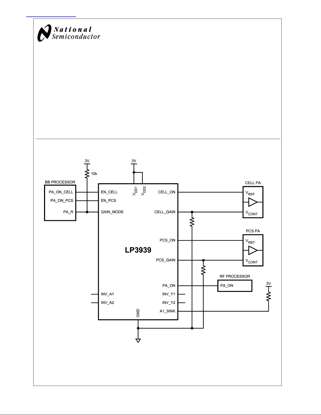
LP3939 Application Circuit
Features
n Power-switch for dual band CDMA power amplifier
Key Specifications
n 0.002 µA Quiescent Current (typ)
n LLP16 Package
Applications
n Dual-band CDMA phones with MSM3xxx or MSM5xxx
platform
Note: This application circuit shows the connection interface to a typical Skyworks PA. Connections to other PA vendors may vary slightly.
© 2003 National Semiconductor Corporation DS200831 www.national.com
20083101
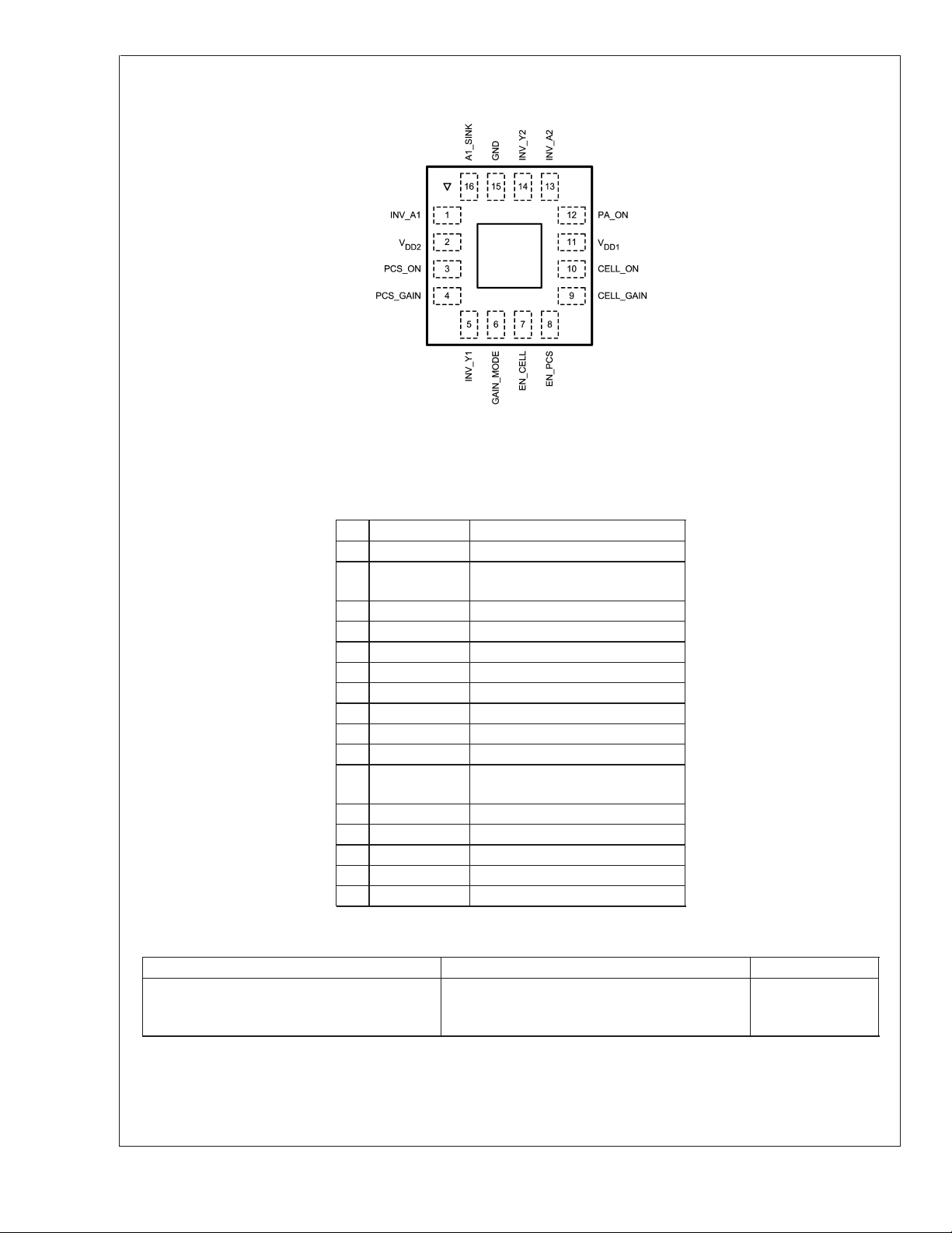
Connection Diagram
LP3939
(LLP16: NSC Marketing Drawing LQA16A)
Pin Description
Top View
20083102
See NS Package Number LQA16A
Pin Name Functional Description
1 INV_A1 Input
2V
DD2
Supply. V
DD1
and V
DD2
must be
tied together externally.
3 PCS_ON Output, open drain
4 PCS_GAIN Output, open drain
5 INV_Y1 Output
6 GAIN_MODE Input
7 EN_CELL Input
8 EN_PCS Input
9 CELL_GAIN Output, open drain
10 CELL_ON Output, open drain
11 V
DD1
Supply. V
DD1
and V
DD2
must be
tied together externally.
12 PA_ON Output
13 INV_A2 Input
14 INV_Y2 Output, open drain
15 GND GND
16 A1_SINK Output, open drain
Ordering Information
LP3939 Supplied as 1k Units, Tape and Reel LP3939 Supplied as 4.5k Units, Tape and Reel Package Marking
LP3939ILQ LP3939ILQX National Logo
Note:
U-wafer fab code
Z-assembly plant code
XY-date code
TT-die run traceability
www.national.com 2
UZXYTT
LP3939
LP3939
Absolute Maximum Ratings (Notes 1,
2)
If Military/Aerospace specified devices are required,
please contact the National Semiconductor Sales Office/
Storage Temperature −65˚C to +150˚C
ESD (Note 4):
Human Body Model 2 kV
Machine Model 200V
Distributors for availability and specifications.
V
DD1,VDD2
EN_CELL, EN_PCS,
GAIN_MODE, INV_A1,
INV_A2, PA_ON, INV_Y1,
CELL_ON, CELL_GAIN,
PCS_ON, PCS_GAIN, INV_Y2
and A1_SINK −0.3V to (V
GND to GND SLUG
Junction Temperature 150˚C
−0.3V to +6.0V
+ 0.3V)
DD
±
0.3V
Operating Ratings (Notes 1, 2)
V
DD1,VDD2
Junction Temperature −40˚C to +125˚C
Operating Temperature −40˚C to +85˚C
Thermal Resistance
θ
(LLP16)
JA
Maximum Power Dissipation
(Note 5) 1.38W
Maximum Power Dissipation
(Note 3) 2.0W
DC Electrical Characteristics
Unless otherwise noted, V
DD1=VDD2
pearing in boldface type apply over the entire junction temperature range for operation, −40˚C to +85˚C. (Note 6)
Symbol Parameter Conditions Typ
I
IN
I
Q
I
LEAKAGE
R
DS-ON
V
IH
V
IL
V
OH
V
OL
Input Current All Input Pins 0.05 5 µA
Quiescent Current All inputs tied to VDDor ground.
Output Leakage Current CELL_ON, PCS_ON
MOSFET’s ON Resistance P-Ch, VDD=3V
Logic High Input 1.8V ≤ V
Logic Low Input 1.8V ≤ VDD≤ 3.5V
Logic High Output PA_ON, INV_Y1,
Logic Low Output PA_ON, INV_Y1, I
= 3V. Typical values and limits appearing in normal type apply for TJ= 25˚C. Limits ap-
Limit
Min Max
No load at the outputs.
0.002 5 µA
CELL_GAIN, PCS_GAIN
A1_SINK 5
CELL_ON, PCS_ON
275 500
CELL_GAIN, PCS_GAIN
DD
=2V
430 650
P-Ch, V
CELL_ON, PCS_ON
CELL_GAIN, PCS_GAIN
<
2.5V
DD
EN_CELL, EN_PCS, INV_A1,
1.4
GAIN_MODE, INV_A2
2.5V ≤ V
EN_CELL, EN_PCS, INV_A1,
DD
≤ 3.5V
2.0
GAIN_MODE, INV_A2
EN_CELL, EN_PCS, INV_A1,
GAIN_MODE, INV_A2
I
SOURCE
=1mA
INV_Y2,
I
SOURCE
=1mA
INV_Y2, A1_SINK
=1mA
I
SINK
=1mA 80 200
SINK
2.93 2.8
2.74 2.5
16 55
1.8V to 5.5V
39.8˚C/W
Units
10
mΩ
0.4 V
mV
µA
V
V
www.national.com3

AC Electrical Characteristics
Unless otherwise noted, V
LP3939
25˚C. Limits appearing in boldface type apply over the entire junction temperature range for operation, −40˚C to +85˚C.
DD1=VDD2
(Note 7)
Symbol Parameter Conditions Typ
t
PLH
Propagations Delay
Low to High
t
PHL
Propagations Delay
High to Low
t
RISE
T
FALL
Note 1: Absolute Maximum Ratings are limits beyond which damage to the device may occur. Operating Ratings are conditions under which operation of the device
is guaranteed. Operating Ratings do not imply guaranteed performance limits. For guaranteed performance limits and associated test conditions, see the Electrical
Characteristics tables.
Note 2: All voltages are with respect to the potential at the GND pin.
Note 3: The Absolute Maximum power dissipation depends on the ambient temperature and can be calculated using the formula:
Rise Time PA_ON 15 120
Fall Time PA_ON 15 120
= 3V, C
= 50 pF. Typical values and limits appearing in normal type apply for TJ=
LOAD
Limit
Min Max
EN_CELL to PA_ON or
EN_PCS to PA_ON
10 80 ns
EN_CELL to CELL_ON or
EN_PCS to PCS_ON
= 100Ω
R
PD
7 56 ns
GAIN_MODE to CELL_GAIN
or GAIN_MODE to PCS_GAIN
= 100Ω
R
PD
7 56 ns
INV_A1 to INV_Y1 10 80 ns
INV_A2 to INV_Y2 25 200 ns
EN_CELL to PA_ON or
EN_PCS to PA_ON
10 80 ns
EN_CELL to CELL_ON or
EN_PCS to PCS_ON
= 100Ω
R
PD
25 200 ns
GAIN_MODE to CELL_GAIN
or GAIN_MODE to PCS_GAIN
= 100Ω
R
PD
20 160 ns
INV_A1 to INV_Y1 10 80 ns
INV_A1 to A1_SINK
R
=10kΩ
PU
5 40 ns
INV_A2 to INV_Y2 5 40 ns
INV_Y1 20 160
INV_Y1 20 160
Units
nsINV_Y2 50 400
nsINV_Y2 10 80
where TJis the junction temperature, TAis the ambient temperature, and θJAis the junction-to-ambient temperature. The 2.0W rating appearing under Absolute
Maximum Ratings results from substituting the Absolute Maximum junction temperature, 150˚C for T
dissipated safely at ambient temperatures below 70˚C. Less power can be dissipated safely at ambient temperatures above 70˚C. The Absolute Maximum power
dissipation can be increased by 25 mW for each degree below 70˚C, and it must be derated by 25 mW for each degree above 70˚C.
Note 4: The human body model is 100 pF discharged through a 1.5 kΩ resistor into each pin. The machine model is a 200 pF capacitor discharged directly into
each pin.
Note 5: Like the Absolute Maximum power dissipation, the maximum power dissipation depends on the ambient temperature. The 1.38W rating appearing under
Absolute Maximum Ratings results from substituting the Maximum junction temperature, 125˚C for T
dissipated safely at ambient temperatures below 70˚C. Less power can be dissipated safely at ambient temperatures above 70˚C. The Absolute Maximum power
dissipation can be increased by 25 mW for each degree below 70˚C, and it must be derated by 25 mW for each degree above 70˚C.
Note 6: All limits are guaranteed by testing or statistical analysis.
Note 7: All AC parameters are guaranteed by design, not production tested.
www.national.com 4
, 70˚C for TAand 39.8˚C/W for θJA. More power can be
J
, 70˚C for TAand 39.8˚C/W for θJA. More power can be
J

LP3939 Block Diagram
LP3939
Truth Tables
TABLE 1. PA Enables
INPUTS OUTPUTS
EN_CELL EN_PCS CELL_ON PCS_ON PA_ON
000 00
101 01
010 11
1 1 Not Valid
Note: Measured with a 10 kΩ pull down resistor on CELL_ON and PCS_ON.
20083104
www.national.com5

Truth Tables (Continued)
LP3939
INPUTS OUTPUTS
GAIN_MODE EN_CELL EN_PCS CELL_GAIN PCS_GAIN
0000 0
0101 0
1100 0
0010 1
1010 0
X 1 1 Not Valid
Note: Measured with a 10 kΩ pull down resistor on CELL_GAIN and PCS_GAIN.
TABLE 3. Current Sink Control
INPUTS OUTPUTS
INV_A1 INV_Y1 A1_SINK
01 0
10 1
INV_A2 INV_Y2
01
10
Note: Measured with a 10 kΩ pull up resistor on A1_SINK.
TABLE 2. PA Gain Mode
www.national.com 6

Physical Dimensions inches (millimeters) unless otherwise noted
LP3939 Power Amplifier Driver for Dual Band CDMA Handsets
NOTES: UNLESS OTHERWISE SPECIFIED
1. STANDARD LEAD FINISH TO BE 5.08 MICROMETERS MINIMUM LEAD/TIN (SOLDER) ON COPPER.
2. NO JEDEC REGISTRATION AS OF APRIL 2000.
16-Lead Plastic Quad Package
Order Number LP3939ILQ or LP3939ILQX
NS Package Number LQA16A
LIFE SUPPORT POLICY
NATIONAL’S PRODUCTS ARE NOT AUTHORIZED FOR USE AS CRITICAL COMPONENTS IN LIFE SUPPORT
DEVICES OR SYSTEMS WITHOUT THE EXPRESS WRITTEN APPROVAL OF THE PRESIDENT AND GENERAL
COUNSEL OF NATIONAL SEMICONDUCTOR CORPORATION. As used herein:
1. Life support devices or systems are devices or
systems which, (a) are intended for surgical implant
into the body, or (b) support or sustain life, and
whose failure to perform when properly used in
accordance with instructions for use provided in the
2. A critical component is any component of a life
support device or system whose failure to perform
can be reasonably expected to cause the failure of
the life support device or system, or to affect its
safety or effectiveness.
labeling, can be reasonably expected to result in a
significant injury to the user.
BANNED SUBSTANCE COMPLIANCE
National Semiconductor certifies that the products and packing materials meet the provisions of the Customer Products
Stewardship Specification (CSP-9-111C2) and the Banned Substances and Materials of Interest Specification
(CSP-9-111S2) and contain no ‘‘Banned Substances’’ as defined in CSP-9-111S2.
National Semiconductor
Americas Customer
Support Center
Email: new.feedback@nsc.com
Tel: 1-800-272-9959
www.national.com
National does not assume any responsibility for use of any circuitry described, no circuit patent licenses are implied and National reserves the right at any time without notice to change said circuitry and specifications.
National Semiconductor
Europe Customer Support Center
Fax: +49 (0) 180-530 85 86
Email: europe.support@nsc.com
Deutsch Tel: +49 (0) 69 9508 6208
English Tel: +44 (0) 870 24 0 2171
Français Tel: +33 (0) 1 41 91 8790
National Semiconductor
Asia Pacific Customer
Support Center
Email: ap.support@nsc.com
National Semiconductor
Japan Customer Support Center
Fax: 81-3-5639-7507
Email: jpn.feedback@nsc.com
Tel: 81-3-5639-7560

Copyright © Each Manufacturing Company.
All Datasheets cannot be modified without permission.
This datasheet has been download from :
www.AllDataSheet.com
100% Free DataSheet Search Site.
Free Download.
No Register.
Fast Search System.
www.AllDataSheet.com
 Loading...