

LP3881
0.8A Fast-Response Ultra Low Dropout Linear
Regulators
LP3881 0.8A Fast-Response Ultra Low Dropout Linear Regulators
August 2003
General Description
The LP3881 is a high current, fast response regulator which
can maintain output voltage regulation with minimum input to
output voltage drop. Fabricated on a CMOS process, the
device operates from two input voltages: Vbias provides
voltage to drive the gate of the N-MOS power transistor,
while Vin is the input voltage which supplies power to the
load. The use of an external bias rail allows the part to
operate from ultra low Vin voltages. Unlike bipolar regulators, the CMOS architecture consumes extremely low quiescent current at any output load current. The use of an
N-MOS power transistor results in wide bandwidth, yet minimum external capacitance is required to maintain loop stability.
The fast transient response of these devices makes them
suitable for use in powering DSP, Microcontroller Core voltages and Switch Mode Power Supply post regulators. The
parts are available in TO-220 and TO-263 packages.
@
Dropout Voltage: 75 mV (typ)
Ground Pin Current: 3 mA (typ) at full load.
Shutdown Current: 60 nA (typ) when S/D pin is low.
Precision Output Voltage: 1.5% room temperature accu-
racy.
0.8A load current.
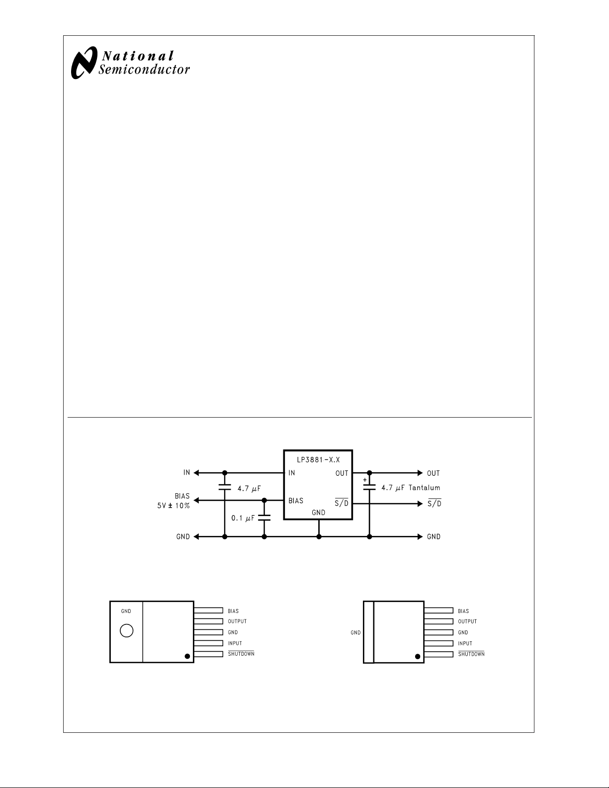
Typical Application Circuit
Features
n Ultra low dropout voltage (75 mV@0.8A typ)
n Low ground pin current
n Load regulation of 0.04%/A
n 60 nA typical quiescent current in shutdown
n 1.5% output accuracy (25˚C)
n TO-220, TO-263 packages
n Over temperature/over current protection
n −40˚C to +125˚C junction temperature range
Applications
n DSP Power Supplies
n Server Core and I/O Supplies
n PC Add-in-Cards
n Local Regulators in Set-Top Boxes
n Microcontroller Power Supplies
n High Efficiency Power Supplies
n SMPS Post-Regulators
At least 4.7 µF of input and output capacitance is required for stability.
20063001
Connection Diagrams
TO-220, Top View
© 2003 National Semiconductor Corporation DS200630 www.national.com
20063002
TO-263, Top View
20063003
Ordering Information
LP3881
Order Number Package Type Package Drawing Supplied As
LP3881ES-1.2 TO263-5 TS5B Rail
LP3881ESX-1.2 TO263-5 TS5B Tape and Reel
LP3881ET-1.2 TO220-5 T05D Rail
LP3881ES-1.5 TO263-5 TS5B Rail
LP3881ESX-1.5 TO263-5 TS5B Tape and Reel
LP3881ET-1.5 TO220-5 T05D Rail
LP3881ES-1.8 TO263-5 TS5B Rail
LP3881ESX-1.8 TO263-5 TS5B Tape and Reel
LP3881ET-1.8 TO220-5 T05D Rail
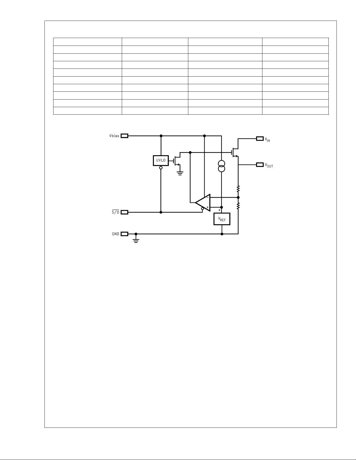
Block Diagram
20063024
www.national.com 2
LP3881
Absolute Maximum Ratings (Note 1)
If Military/Aerospace specified devices are required,
please contact the National Semiconductor Sales Office/
Distributors for availability and specifications.
Storage Temperature Range −65˚C to +150˚C
I
(Survival) Internally Limited
OUT
Output Voltage (Survival) −0.3V to +6V
Junction Temperature −40˚C to +150˚C
Operating Ratings
Lead Temp. (Soldering, 5 seconds) 260˚C
ESD Rating
Human Body Model (Note 3)
Machine Model (Note 10)
2kV
200V
Power Dissipation (Note 2) Internally Limited
Supply Voltage (Survival) −0.3V to +6V
V
IN
V
Supply Voltage (Survival) −0.3V to +7V
BIAS
VINSupply Voltage (V
Shutdown Input Voltage 0 to +6V
I
OUT
Operating Junction
Temperature Range
V
BIAS
Shutdown Input Voltage (Survival) −0.3V to +7V
Electrical Characteristics Limits in standard typeface are for T
over the full operating temperature range. Unless otherwise specified: V
C
OUT
= 4.7 µF, V
S/D=VBIAS
.
Symbol Parameter Conditions
BIAS
<
0.8A
L
≤ 6V
V
∆V
O
Output Voltage Tolerance 10 mA<I
(NOM) + 1V ≤ VIN≤ 5.5V
V
O
4.5V ≤ V
/∆V
O
Output Voltage Line Regulation
IN
VO(NOM) + 1V ≤ VIN≤ 5.5V
(Note 7)
∆VO/∆I
L
Output Voltage Load Regulation
10 mA<I
<
0.8A 0.04
L
(Note 8)
V
DO
IQ(VIN) Quiescent Current Drawn from
I
Q(VBIAS
I
SC
Dropout Voltage (Note 9) IL= 0.8A
Supply
V
IN
) Quiescent Current Drawn from
Supply
V
BIAS
Short-Circuit Current V
<
10 mA
V
S/D
10 mA
V
S/D
OUT
<
I
0.8A
L
≤ 0.3V
<
<
I
0.8A
L
≤ 0.3V
= 0V 1.8 A
Shutdown Input
V
SDT
Output Turn-off Threshold Output = ON 0.7 1.3
Output = OFF 0.7 0.3
Td (OFF) Turn-OFF Delay R
Td (ON) Turn-ON Delay R
I
S/D
S/D Input Current V
XC
LOAD
XC
LOAD
=1.3V 1
S/D
V
≤ 0.3V −1
S/D
OUT
OUT
<<
<<
IN=VO
Td (OFF) 20
Td (ON) 15
OUT+VDO
) to 5.5V
0.8A
−40˚C to +125˚C
Supply Voltage 4.5V to 6V
= 25˚C, and limits in boldface type apply
J
(NOM) + 1V, V
Typical
(Note 4)
= 4.5V, IL= 10 mA, CIN=
BIAS
MIN
(Note 5)
1.198
MAX
(Note 5)
1.234
Units
1.216
1.186
1.478
1.246
1.522
V1.5
1.455
1.773
1.545
1.827
1.8
1.746
1.854
0.01 %/V
0.06
75
3
0.03
1
0.03
120
160
7
8
1
30
2
3
1
30
%/A
mV
mA
µA
mA
µA
V
µs
µA
www.national.com3
Electrical Characteristics Limits in standard typeface are for T
over the full operating temperature range. Unless otherwise specified: V
LP3881
C
OUT
= 4.7 µF, V
S/D=VBIAS
. (Continued)
IN=VO
= 25˚C, and limits in boldface type apply
J
(NOM) + 1V, V
= 4.5V, IL= 10 mA, CIN=
BIAS
Symbol Parameter Conditions
Typical
(Note 4)
MIN
(Note 5)
MAX
(Note 5)
AC Parameters
PSRR (V
PSRR
(V
BIAS
) Ripple Rejection for VINInput
IN
Voltage
Ripple Rejection for V
)
Voltage
BIAS
VIN=V
OUT
VIN=V
OUT
V
BIAS=VOUT
V
BIAS=VOUT
+1V, f = 120 Hz
80
+ 1V, f = 1 kHz 65
+ 3V, f = 120 Hz
70
+ 3V, f = 1 kHz 65
Output Noise Density f = 120 Hz 1 µV/root−Hz
e
n
Note 1: Absolute maximum ratings indicate limits beyond which damage to the component may occur. Operating ratings indicate conditions for which the device
is intended to be functional, but do not guarantee specific performance limits. For guaranteed specifications, see Electrical Characteristics. Specifications do not
apply when operating the device outside of its rated operating conditions.
Note 2: At elevated temperatures, device power dissipation must be derated based on package thermal resistance and heatsink thermal values. θ
devices is 65˚C/W if no heatsink is used. If the TO-220 device is attached to a heatsink, a θ
approximately 40˚C/W if soldered down to a copper plane which is at least 1.5 square inches in area. If power dissipation causes the junction temperature to exceed
specified limits, the device will go into thermal shutdown.
Note 3: The human body model is a 100 pF capacitor discharged through a 1.5k resistor into each pin.
Note 4: Typical numbers represent the most likely parametric norm for 25˚C operation.
Note 5: Limits are guaranteed through testing, statistical correlation, or design.
Note 6: If used in a dual-supply system where the regulator load is returned to a negative supply, the output pin must be diode clamped to ground.
Note 7: Output voltage line regulation is defined as the change in output voltage from nominal value resulting from a change in input voltage.
Note 8: Output voltage load regulation is defined as the change in output voltage from nominal value as the load current increases from no load to full load.
Note 9: Dropout voltage is defined as the minimum input to output differential required to maintain the output with 2% of nominal value.
Note 10: The machine model is a 220 pF capacitor discharged directly into each pin. The machine model ESD rating of pin 5 is 100V.
Output Noise Voltage
= 1.8V
V
OUT
BW = 10 Hz − 100 kHz 150
BW = 300 Hz − 300 kHz 90
value of 4˚C/W can be assumed. θ
J-S
for TO-220
J-A
for TO-263 devices is
J-A
µV (rms)
Units
dB
www.national.com 4

Typical Performance Characteristics
Unless otherwise specified: TA= 25˚C, C
= 4.7µF, S/D pin is tied to V
BIAS,VIN
= 2.2V, V
= 4.7µF, Cin
OUT
OUT
= 1.8V
LP3881
Dropout vs I
V
vs Temperature DC Load Regulation
OUT
L
20063004
I
GND
vs VSD
20063005
Line Regulation vs V
20063006
IN
20063008 20063009
Line Regulation vs V
20063007
BIAS
www.national.com5

Typical Performance Characteristics Unless otherwise specified: T
4.7µF, S/D pin is tied to V
LP3881
vs I
= 2.2V, V
L
BIAS,VIN
I
BIAS
Noise Measurement V
= 1.8V (Continued)
OUT
20063010
= 25˚C, C
A
I
vs VSD
GND
Startup Waveform
OUT
= 4.7µF, Cin =
OUT
20063012
20063014
Line Regulation vs V
BIAS
20063018
www.national.com 6
Line Regulation vs V
20063015
BIAS
20063019

LP3881
Typical Performance Characteristics Unless otherwise specified: T
4.7µF, S/D pin is tied to V
BIAS,VIN
= 2.2V, V
VINPSRR VINPSRR
V
PSRR
BIAS
= 1.8V (Continued)
OUT
20063020 20063023
= 25˚C, C
A
= 4.7µF, Cin =
OUT
20063022
www.national.com7

Application Hints
LP3881
V
RESTRICTIONS FOR PROPER START-UP
BIAS
To prevent misoperation, ensure that V
before start-up is initiated. This scenario can occur in systems with a backup battery using reverse-biased "blocking"
diodes which may allow enough leakage current to flow into
the V
node to raise it’s voltage slightly above ground
BIAS
when the main power is removed. Using low leakage diodes
or a resistive pull down can prevent the voltage at V
rising above 50mV. Large bulk capacitors connected to
may also cause a start-up problem if they do not
V
BIAS
discharge fully before re-start is initiated (but only if V
allowed to fall below 1V). A resistor connected across the
capacitor will allow it to discharge more quickly. It should be
noted that the probability of a "false start" caused by incorrect logic states is extremely low.
EXTERNAL CAPACITORS
To assure regulator stability, input and output capacitors are
required as shown in the Typical Application Circuit.
OUTPUT CAPACITOR
At least 4.7µF of output capacitance is required for stability
(the amount of capacitance can be increased without limit).
The output capacitor must be located less than 1 cm from
the output pin of the IC and returned to a clean analog
ground. The ESR (equivalent series resistance) of the output
capacitor must be within the "stable" range as shown in the
graph below over the full operating temperature range for
stable operation.
is below 50mV
BIAS
BIAS
BIAS
from
Because the ESR of ceramic capacitors is only a few milli
Ohms, they are not suitable for use as output capacitors on
LP388X devices. The regulator output can tolerate ceramic
capacitance totaling up to 15% of the amount of Tantalum
capacitance connected from the output to ground.
OUTPUT "BYPASS" CAPACITORS
Many designers place small value "bypass" capacitors at
various circuit points to reduce noise. Ceramic capacitors in
the value range of about 1000pF to 0.1µF placed directly on
the output of a PNP or P-FET LDO regulator can cause a
loss of phase margin which can result in oscillations, even
is
when a Tantalum output capacitor is in parallel with it. This is
not unique to National Semiconductor LDO regulators, it is
true of any P-type LDO regulator.
The reason for this is that PNP or P-FET regulators have a
higher output impedance (compared to an NPN regulator),
which results in a pole-zero pair being formed by every
different capacitor connected to the output.
The zero frequency is approximately:
=1/(2Xπ XESRXC)
F
z
Where ESR is the equivalent series resistance of the capacitor, and C is the value of capacitance.
The pole frequency is:
=1/(2Xπ XRLXC)
F
p
Where R
is the load resistance connected to the regulator
L
output.
To understand why a small capacitor can reduce phase
margin: assume a typical LDO with a bandwidth of 1MHz,
which is delivering 0.5A of current from a 2.5V output (which
means R
is 5 Ohms). We then place a .047 µF capacitor on
L
the output. This creates a pole whose frequency is:
=1/(2Xπ X 5 X .047 X 10E-6) = 677 kHz
F
p
This pole would add close to 60 degrees of phase lag at the
crossover (unity gain) frequency of 1 MHz, which would
almost certainly make this regulator oscillate. Depending on
the load current, output voltage, and bandwidth, there are
usually values of small capacitors which can seriously reduce phase margin. If the capacitors are ceramic, they tend
to oscillate more easily because they have very little internal
inductance to damp it out. If bypass capacitors are used, it is
best to place them near the load and use trace inductance to
"decouple" them from the regulator output.
Minimum ESR vs Output Load Current
20063031
Tantalum capacitors are recommended for the output as
their ESR is ideally suited to the part’s requirements and the
ESR is very stable over temperature. Aluminum electrolytics
are not recommended because their ESR increases very
rapidly at temperatures below 10C. Aluminum caps can only
be used in applications where lower temperature operation
is not required.
A second problem with Al caps is that many have ESR’s
which are only specified at low frequencies. The typical loop
bandwidth of a linear regulator is a few hundred kHz to
several MHz. If an Al cap is used for the output cap, it must
be one whose ESR is specified at a frequency of 100 kHz or
more.
www.national.com 8
INPUT CAPACITOR
The input capacitor must be at least 4.7 µF, but can be
increased without limit. It’s purpose is to provide a low
source impedance for the regulator input. Ceramic capacitors work best for this, but Tantalums are also very good.
There is no ESR limitation on the input capacitor (the lower,
the better). Aluminum electrolytics can be used, but their
ESR increase very quickly at cold temperatures. They are
not recommended for any application where temperatures
go below about 10˚C.
BIAS CAPACITOR
The 0.1µF capacitor on the bias line can be any good quality
capacitor (ceramic is recommended).
BIAS VOLTAGE
The bias voltage is an external voltage rail required to get
gate drive for the N-FET pass transistor. Bias voltage must
be in the range of 4.5 - 6V to assure proper operation of the
part.

Application Hints (Continued)
UNDER VOLTAGE LOCKOUT
The bias voltage is monitored by a circuit which prevents the
regulator output from turning on if the bias voltage is below
approximately 4V.
SHUTDOWN OPERATION
Pulling down the shutdown (S/D) pin will turn-off the regulator. Pin S/D must be actively terminated through a pull-up
resistor (10 kΩ to 100 kΩ) for a proper operation. If this pin
is driven from a source that actively pulls high and low (such
as a CMOS rail to rail comparator), the pull-up resistor is not
required. This pin must be tied to Vin if not used.
POWER DISSIPATION/HEATSINKING
A heatsink may be required depending on the maximum
power dissipation and maximum ambient temperature of the
application. Under all possible conditions, the junction temperature must be within the range specified under operating
conditions. The total power dissipation of the device is given
by:
=(VIN−V
P
D
where I
OUT)IOUT
is the operating ground current of the device.
GND
The maximum allowable temperature rise (T
on the maximum ambient temperature (T
cation, and the maximum allowable junction temperature
):
(T
Jmax
=T
T
Rmax
Jmax−TAmax
The maximum allowable value for junction to ambient Thermal Resistance, θ
θ
JA=TRmax/PD
These parts are available in TO-220 and TO-263 packages.
The thermal resistance depends on amount of copper area
or heat sink, and on air flow. If the maximum allowable value
calculated above is ≥ 60 ˚C/W for TO-220 package
of θ
JA
and ≥ 60 ˚C/W for TO-263 package no heatsink is needed
since the package can dissipate enough heat to satisfy these
requirements. If the value for allowable θ
limits, a heat sink is required.
+(VIN)I
GND
) depends
Rmax
) of the appli-
Amax
, can be calculated using the formula:
JA
falls below these
JA
The heatsink to be used in the application should have a
heatsink to ambient thermal resistance,
θ
HA≤θJA
In this equation, θ
to the surface of the heat sink and θ
tance from the junction to the surface of the case. θ
about 3˚C/W for a TO220 package. The value for θ
pends on method of attachment, insulator, etc. θ
− θCH− θJC.
CH
is the thermal resistance from the case
is the thermal resis-
JC
JC
de-
CH
varies
CH
between 1.5˚C/W to 2.5˚C/W. If the exact value is unknown,
2˚C/W can be assumed.
HEATSINKING TO-263 PACKAGE
The TO-263 package uses the copper plane on the PCB as
a heatsink. The tab of these packages are soldered to the
copper plane for heat sinking. The graph below shows a
curve for the θ
of TO-263 package for different copper area
JA
sizes, using a typical PCB with 1 ounce copper and no solder
mask over the copper area for heat sinking.
20063025
FIGURE 1. θJAvs Copper (1 Ounce) Area for TO-263
package
LP3881
is
HEATSINKING TO-220 PACKAGE
The thermal resistance of a TO220 package can be reduced
by attaching it to a heat sink or a copper plane on a PC
board. If a copper plane is to be used, the values of θ
will
JA
be same as shown in next section for TO263 package.
www.national.com9

Application Hints (Continued)
LP3881
As shown in the graph below, increasing the copper area
beyond 1 square inch produces very little improvement. The
minimum value for θ
PCB is 32˚C/W.
Figure 2 shows the maximum allowable power dissipation
for TO-263 packages for different ambient temperatures,
assuming θ
is 35˚C/W and the maximum junction tempera-
JA
ture is 125˚C.
for the TO-263 package mounted to a
JA
20063026
FIGURE 2. Maximum power dissipation vs ambient
temperature for TO-263 package
www.national.com 10

Physical Dimensions inches (millimeters) unless otherwise noted
LP3881
TO220 5-lead, Molded, Stagger Bend Package (TO220-5)
NS Package Number T05D
www.national.com11

Physical Dimensions inches (millimeters) unless otherwise noted (Continued)
TO263 5-Lead, Molded, Surface Mount Package (TO263-5)
NS Package Number TS5B
LP3881 0.8A Fast-Response Ultra Low Dropout Linear Regulators
LIFE SUPPORT POLICY
NATIONAL’S PRODUCTS ARE NOT AUTHORIZED FOR USE AS CRITICAL COMPONENTS IN LIFE SUPPORT
DEVICES OR SYSTEMS WITHOUT THE EXPRESS WRITTEN APPROVAL OF THE PRESIDENT AND GENERAL
COUNSEL OF NATIONAL SEMICONDUCTOR CORPORATION. As used herein:
1. Life support devices or systems are devices or
systems which, (a) are intended for surgical implant
into the body, or (b) support or sustain life, and
whose failure to perform when properly used in
accordance with instructions for use provided in the
labeling, can be reasonably expected to result in a
significant injury to the user.
National Semiconductor
Americas Customer
Support Center
Email: new.feedback@nsc.com
Tel: 1-800-272-9959
www.national.com
National Semiconductor
Europe Customer Support Center
Fax: +49 (0) 180-530 85 86
Email: europe.support@nsc.com
Deutsch Tel: +49 (0) 69 9508 6208
English Tel: +44 (0) 870 24 0 2171
Français Tel: +33 (0) 1 41 91 8790
2. A critical component is any component of a life
support device or system whose failure to perform
can be reasonably expected to cause the failure of
the life support device or system, or to affect its
safety or effectiveness.
National Semiconductor
Asia Pacific Customer
Support Center
Email: ap.support@nsc.com
National Semiconductor
Japan Customer Support Center
Fax: 81-3-5639-7507
Email: jpn.feedback@nsc.com
Tel: 81-3-5639-7560
National does not assume any responsibility for use of any circuitry described, no circuit patent licenses are implied and National reserves the right at any time without notice to change said circuitry and specifications.
 Loading...