

May 2005
LP3878-ADJ
Micropower 800mA Low Noise "Ceramic Stable"
Adjustable Voltage Regulator for 1V to 5V Applications
LP3878-ADJ Micropower 800mA Low Noise "Ceramic Stable" Adjustable Voltage Regulator for 1V
to 5V Applications
General Description
The LP3878-ADJ is an 800 mA adjustable output voltage
regulator designed to provide high performance and low
noise in applications requiring output voltages as low as
1.0V.
™
Using an optimized VIP
cess, the LP3878-ADJ delivers superior performance:
Ground Pin Current: Typically 5.5 mA
180 µA
Low Power Shutdown: The LP3878-ADJ draws less than
10 µA quiescent current when shutdown pin is pulled low.
Precision Output: Guaranteed output voltage accuracy is
1% at room temperature.
Low Noise: Broadband output noise is only 18 µV (typical)
with 10 nF bypass capacitor.
@
100 µA load.
(Vertically Integrated PNP) pro-
@
800 mA load, and
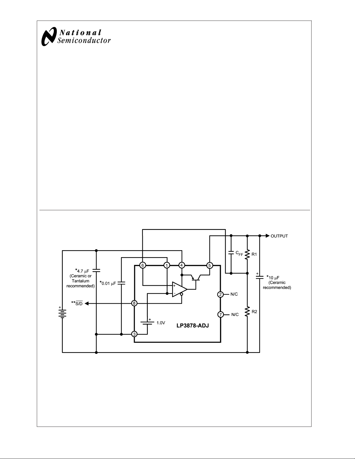
Basic Application Circuit
Features
n 1.0V to 5.5V output
n Designed for use with low ESR ceramic capacitors
n Very low output noise
n 8 Lead PSOP and LLP surface mount package
<
n
10 µA quiescent current in shutdown
n Low ground pin current at all loads
n Over-temperature/over-current protection
n -40˚C to +125˚C operating junction temperature range
Applications
n ASIC Power Supplies In:
- Desktops, Notebooks and Graphic Cards
- Set Top Boxes, Printers and Copiers
n DSP and FPGA Power Supplies
n SMPS Post-Regulator
n Medical Instrumentation
*Capacitance values shown are minimum required to assure stability. Larger output capacitor provides improved dynamic response. Output capacitor must
meet ESR requirements (see Application Information).
**The Shutdown pin must be actively terminated (see Application Information). Tie to INPUT (Pin 4) if not used.
VIP™is a trademark of National Semiconductor Corporation.
© 2005 National Semiconductor Corporation DS201209 www.national.com
20120903
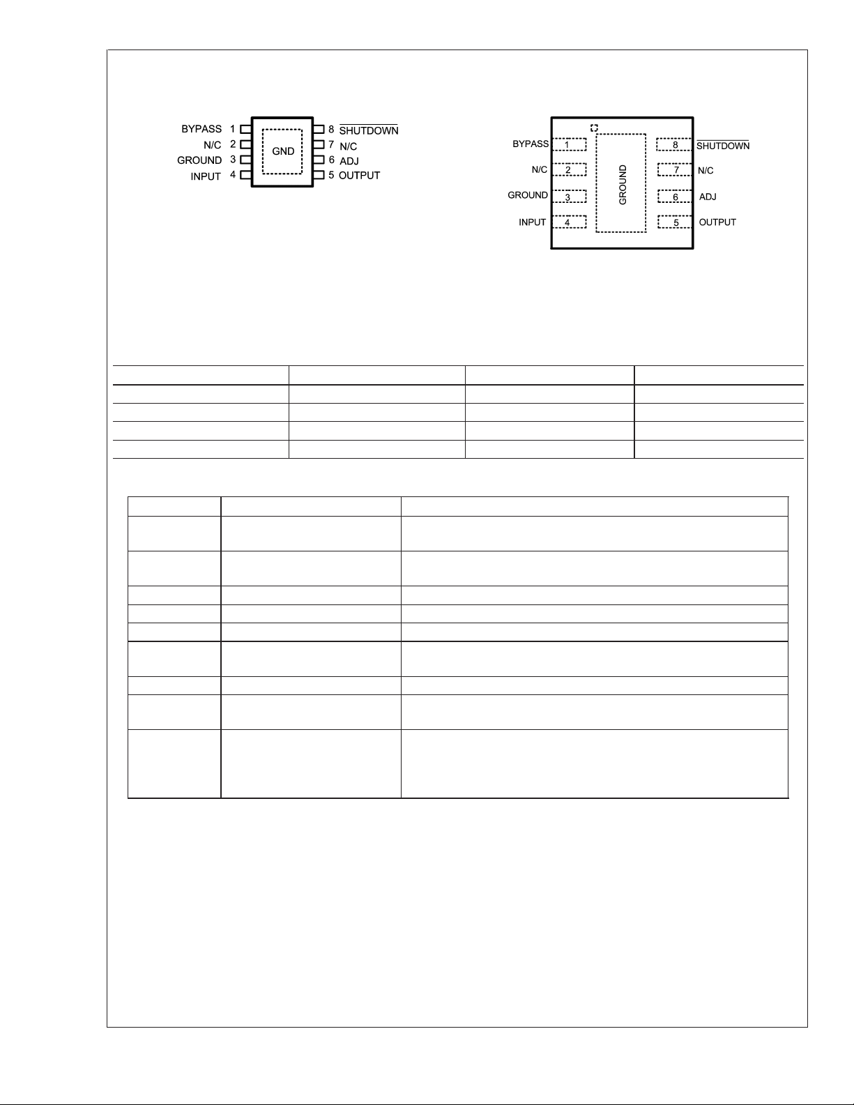
Connection Diagrams
8 Lead PSOP Package (MRA) 8 Lead LLP Surface Mount Package (SD)
LP3878-ADJ
Top View
See NS Package Number MRA08A
20120930
Top View
See NS Package Number SDC08A
Ordering Information
TABLE 1. Package Marking and Ordering Information
Output Voltage Grade Order Information Supplied as:
ADJ STD LP3878MR-ADJ 95 Units per Rail
ADJ STD LP3878MRX-ADJ 2500 Units on Tape and Reel
ADJ STD LP3878SD-ADJ 1000 Units on Tape and Reel
ADJ STD LP3878SDX-ADJ 4500 Units on Tape and Reel
Pin Description
PIN NAME FUNCTION
1 BYPASS The capacitor connected between BYPASS and GROUND lowers
output noise voltage level and is required for loop stability.
2 N/C DO NOT CONNECT. This pin is used for post package test and must
be left floating.
3 GROUND Device ground.
4 INPUT Input source voltage.
5 OUTPUT Regulated output voltage.
6 ADJ Provides feedback to error amplifier from the resistive divider that sets
the output voltage.
7 N/C No internal connection.
8 SHUTDOWN Output is enabled above turn-on threshold voltage. Pull down to turn off
regulator output.
PSOP, LLP
DAP
SUBSTRATE
GROUND
The exposed die attach pad should be connected to a thermal pad at
ground potential. For additional information on using National
Semiconductor’s Non Pull Back LLP package, please refer to LLP
application note AN-1187
20120950
www.national.com 2
LP3878-ADJ
Absolute Maximum Ratings (Note 1)
If Military/Aerospace specified devices are required,
please contact the National Semiconductor Sales Office/
Distributors for availability and specifications.
Storage Temperature Range −65˚C to +150˚C
Operating Junction Temperature
Range -40˚C to +125˚C
Lead Temperature (Soldering, 5
seconds) 260˚C
ESD Rating (Note 2) 2 kV
Power Dissipation (Note 3) Internally Limited
Input Supply Voltage (Survival) −0.3V to +16V
Input Supply Voltage (Typical
Operating) 2.5V to +16V
ADJ Pin −0.3V to +6V
Output Voltage (Survival) (Note 4) −0.3V to +6V
I
(Survival) Short Circuit
OUT
Protected
Input-Output Voltage (Survival)
(Note 5) −0.3V to +16V
Shutdown Pin 1kV
Electrical Characteristics
Limits in standard typeface are for TJ= 25˚C, and limits in boldface type apply over the temperature range of -40˚C to 125˚C.
Limits are guaranteed through design, testing, or correlation. The limits are used to calculate National’s Average Outgoing
Quality Level (AOQL). Unless otherwise specified: V
BYPASS
=10nF.
C
= 3.0V, V
IN
Symbol Parameter Conditions Min Typical Max Units
V
ADJ
Adjust Pin Voltage 0.99 1.00 1.01
Output Voltage Line
1mA≤ I
3.0V ≤ V
3.0V ≤ VIN≤ 16V
≤ 800 mA
L
≤ 6V
IN
Regulation
= 800 mA
I
L
Minimum Input
V
(min)
IN
Voltage Required
To Maintain Output
Regulation
Dropout Voltage
V
DO
I
GND
I
(PK) Peak Output
O
(Note 6)
= 3.8V
V
OUT
Ground Pin Current IL= 100 µA
≥ V
V
OUT
OUT(NOM)
I
= 800 mA
L
≥ V
V
OUT
OUT(NOM)
≤ 125˚C
0 ≤ T
J
I
= 750 mA
L
≥ V
V
OUT
OUT(NOM)
I
= 100 µA 1 2
L
IL= 200 mA 150 200
= 800 mA 475 600
I
L
I
= 200 mA
L
I
= 800 mA
L
V
≥ V
OUT
OUT(NOM)
-1%
-1%
-1%
−5%
Current
IO(MAX) Short Circuit
RL= 0 (Steady State)
Current
e
n
Output Noise
Voltage (RMS)
BW = 100 Hz to 100 kHz
BYPASS
=10nF
C
Ripple Rejection f=1kHz
= 1V, IL= 1 mA, C
OUT
0.98
0.97
= 10 µF, CIN= 4.7 µF, V
OUT
1.00
1.02
1.03
0.014
0.007
0.032
2.5 3.1
2.5 2.8
2.5 3.0
3
300
1100
180
1.5
5.5
200
225
2
3.5
8.5
15
1200
1300
18 µV(RMS)
60 dB
S/D
= 2V,
V
%/V
V
mV
µA
mA
mA
I
ADJ
ADJ Pin Bias
Current (Sourcing)
IL= 800 mA
200 nA
www.national.com3
Electrical Characteristics (Continued)
Limits in standard typeface are for TJ= 25˚C, and limits in boldface type apply over the temperature range of -40˚C to 125˚C.
Limits are guaranteed through design, testing, or correlation. The limits are used to calculate National’s Average Outgoing
Quality Level (AOQL). Unless otherwise specified: V
LP3878-ADJ
C
BYPASS
=10nF.
= 3.0V, V
IN
Symbol Parameter Conditions Min Typical Max Units
SHUTDOWN INPUT
V
S/D
I
S/D
Note 1: Absolute Maximum Ratings indicate limits beyond which damage to the component may occur. Electrical specifications do not apply when operating the
device outside of its rated operating conditions.
Note 2: ESD testing was performed using Human Body Model, a 100 pF capacitor discharged through a 1.5 kΩ resistor.
Note 3: The maximum allowable power dissipation is a function of the maximum junction temperature, T
and the ambient temperature, T
S/D Input Voltage VH= Output ON 1.4 1.6
V
= Output OFF
L
≤ 10 µA
I
IN
V
≤ 10 mV
OUT
≤ 50 µA
I
IN
S/D Input Current V
. The maximum allowable power dissipation at any ambient temperature is calculated using:
A
= 0 0.02 −1
S/D
V
=5V 5 15
S/D
= 1V, IL= 1 mA, C
OUT
= 10 µF, CIN= 4.7 µF, V
OUT
0.04 0.20
0.6
(MAX), the junction-to-ambient thermal resistance, θ
J
S/D
= 2V,
V
µA
J−A
,
The value of θ
vias. If a four layer board is used with maximum vias from the IC center to the heat dissipating copper layers, values of θ
60˚C/W for the PSOP-8 and 40˚C/W for the LLP-8 package. For improved thermal resistance and power dissipation for the LLP package, refer to Application Note
AN-1187. Exceeding the maximum allowable power dissipation will cause excessive die temperature, and the regulator will go into thermal shutdown.
Note 4: If used in a dual-supply system where the regulator load is returned to a negative supply, the LP3878-ADJ output must be diode-clamped to ground.
Note 5: The output PNP structure contains a diode between the V
on this diode and may induce a latch-up mode which can damage the part (see Application Hints).
Note 6: Dropout voltage spec applies only if V
for the LLP (SD) and PSOP (MRA) packages are specifically dependent on PCB trace area, trace material, and the number of layers and thermal
J−A
and V
IN
is sufficient so that it does not limit regulator operation.
IN
terminals that is normally reverse-biased. Forcing the output above the input will turn
OUT
which can be obtained are approximately
J−A
www.national.com 4

LP3878-ADJ
Typical Performance Characteristics Unless otherwise specified: V
= 4.7 µF, C
C
IN
OUT
I
= 10 µF, V
vs Temperature Minimum VINOver Temperature
GND
I
GND
S/D
vs I
= 2V, C
Load
= 10 nF, TJ= 25˚C.
BYP
20120920
V
OUT
= 3.3V, V
IN
OUT
vs Temperature
= 1V, IL= 1 mA,
20120921
Minimum VINvs V
OUT
20120922
20120951
Minimum VINvs V
20120959
OUT
20120952
www.national.com5

Typical Performance Characteristics Unless otherwise specified: V
= 4.7 µF, C
C
IN
OUT
= 10 µF, V
S/D
= 2V, C
= 10 nF, TJ= 25˚C. (Continued)
BYP
= 3.3V, V
IN
= 1V, IL= 1 mA,
OUT
LP3878-ADJ
Minimum V
IN
vs V
OUT
Ripple Rejection
20120953
Ripple Rejection Line Transient Response
20120954
20120958
Line Transient Response Line Transient Response
20120933
www.national.com 6
20120931
20120932

LP3878-ADJ
Typical Performance Characteristics Unless otherwise specified: V
= 4.7 µF, C
C
IN
= 10 µF, V
OUT
S/D
= 2V, C
= 10 nF, TJ= 25˚C. (Continued)
BYP
Line Transient Response Line Transient Response
20120935
Line Transient Response Line Transient Response
= 3.3V, V
IN
= 1V, IL= 1 mA,
OUT
20120936
20120934
Line Transient Response Line Transient Response
20120939
20120937
20120940
www.national.com7

Typical Performance Characteristics Unless otherwise specified: V
= 4.7 µF, C
C
IN
OUT
= 10 µF, V
S/D
= 2V, C
= 10 nF, TJ= 25˚C. (Continued)
BYP
= 3.3V, V
IN
= 1V, IL= 1 mA,
OUT
LP3878-ADJ
Line Transient Response Line Transient Response
20120942
Load Transient Response Load Transient Response
20120941
20120945
Load Transient Response Load Transient Response
20120946
www.national.com 8
20120943
20120944

LP3878-ADJ
Typical Performance Characteristics Unless otherwise specified: V
= 4.7 µF, C
C
IN
= 10 µF, V
OUT
S/D
= 2V, C
= 10 nF, TJ= 25˚C. (Continued)
BYP
Turn-On Characteristics Turn-Off Characteristics
20120955
= 3.3V, V
IN
= 1V, IL= 1 mA,
OUT
20120956
www.national.com9

Block Diagram
LP3878-ADJ
Application Information
PACKAGE INFORMATION
The LP3878-ADJ is offered in the 8 lead PSOP or LLP
surface mount packages to allow for increased power dissipation compared to the SO-8 and Mini SO-8. For details on
thermal performance as well as mounting and soldering
specifications, refer to Application Note AN-1187.
20120901
EXTERNAL CAPACITORS
Like any low-dropout regulator, the LP3878-ADJ requires
external capacitors for regulator stability. These capacitors
must be correctly selected for good performance.
INPUT CAPACITOR: A capacitor whose value is at least 4.7
±
20%) is required between the LP3878-ADJ input and
µF (
ground. A good quality X5R / X7R ceramic capacitor should
be used.
Capacitor tolerance and temperature variation must be considered when selecting a capacitor (see Capacitor Charac-
teristics section) to assure the minimum requirement of
input capacitance is met over all operating conditions.
The input capacitor must be located not more than 0.5" from
the input pin and returned to a clean analog ground. Any
good quality ceramic or tantalum capacitor may be used,
assuming the minimum input capacitance requirement is
met.
OUTPUT CAPACITOR: The LP3878-ADJ requires a ceramic output capacitor whose size is at least 10 µF (
A good quality X5R / X7R ceramic capacitor should be used.
Capacitance tolerance and temperature characteristics must
be considered when selecting an output capacitor.
The LP3878-ADJ is designed specifically to work with ceramic output capacitors, utilizing circuitry which allows the
regulator to be stable across the entire range of output
current with an ultra low ESR output capacitor.
The output capacitor selected must meet the requirement for
minimum amount of capacitance and also have an ESR
(equivalent series resistance) value which is within the
stable range. A curve is provided which shows the stable
ESR range as a function of load current (see Figure 1).
±
20%).
20120938
FIGURE 1. Stable Region For Output Capacitor ESR
Important: The output capacitor must maintain its ESR
within the stable region over the full operating temperature
range of the application to assure stability.
The output capacitor ESR forms a zero which is required to
add phase lead near the loop gain crossover frequency,
typically in the range of 50kHz to 200 kHz. The ESR at lower
frequencies is of no importance. Some capacitor manufacturers list ESR at low frequencies only, and some give a
formula for Dissipation Factor which can be used to calculate
a value for a term referred to as ESR. However, since the DF
formula is usually at a much lower frequency than the range
listed above, it will give an unrealistically high value. If good
quality X5R or X7R ceramic capacitors are used, the actual
ESR in the 50 kHz to 200 kHz range will not exceed 25 milli
Ohms. If these are used as output capacitors for the
LP3878-ADJ, the regulator stability requirements are satisfied.
www.national.com 10

Application Information (Continued)
It is important to remember that capacitor tolerance and
variation with temperature must be taken into consideration
when selecting an output capacitor so that the minimum
required amount of output capacitance is provided over the
full operating temperature range. (See Capacitor Characteristics section).
The output capacitor must be located not more than 0.5"
from the output pin and returned to a clean analog ground.
NOISE BYPASS CAPACITOR: The 10 nF capacitor on the
Bypass pin significantly reduces noise on the regulator output and is required for loop stability. However, the capacitor
is connected directly to a high-impedance circuit in the bandgap reference.
Because this circuit has only a few microamperes flowing in
it, any significant loading on this node will cause a change in
the regulated output voltage. For this reason, DC leakage
current through the noise bypass capacitor must never exceed 100 nA, and should be kept as low as possible for best
output voltage accuracy.
The types of capacitors best suited for the noise bypass
capacitor are ceramic and film. High-quality ceramic capacitors with either NPO or COG dielectric typically have very
low leakage. 10 nF polypropolene and polycarbonate film
capacitors are available in small surface-mount packages
and typically have extremely low leakage current.
FEEDFORWARD CAPACITOR
The feedforward capacitor designated C
plication circuit is required to increase phase margin and
assure loop stability. Improved phase margin also gives
better transient response to changes in load or input voltage,
and faster settling time on the output voltage when transients
occur. C
forms both a pole and zero in the loop gain, the
FF
zero providing beneficial phase lead (which increases phase
margin) and the pole adding undesirable phase lag (which
should be minimized). The zero frequency is determined
both by the value of C
fz=1/(2xπ xC
FF
and R1:
FF
The pole frequency resulting from C
value of C
and the parallel combination of R1 and R2:
FF
fp=1/(2xπ xC
x (R1 // R2))
FF
At higher output voltages where R1 is much greater than R2,
the value of R2 primarily determines the value of the parallel
combination of R1 // R2. This puts the pole at a much higher
frequency than the zero. As the regulated output voltage is
reduced (and the value of R1 decreases), the parallel effect
of R2 diminishes and the two equations become equal (at
which point the pole and zero cancel out). Because the pole
frequency gets closer to the zero at lower output voltages,
the beneficial effects of C
are increased if the frequency
FF
range of the zero is shifted slightly higher for applications
with low Vout (because then the pole adds less phase lag at
the loop’s crossover frequency).
should be selected to place the pole zero pair at a
C
FF
frequency where the net phase lead added to the loop at the
crossover frequency is maximized. The following design
guidelines were obtained from bench testing to optimize
phase margin, transient response, and settling time:
For Vout ≤ 2.5V: C
should be selected to set the zero
FF
frequency in the range of about 50 kHz to 200 kHz.
>
For Vout
2.5V: CFFshould be selected to set the zero
frequency in the range of about 20 kHz to 100 kHz.
in the Basic Ap-
FF
x R1)
is determined by the
FF
CAPACITOR CHARACTERISTICS
CERAMIC: The LP3878-ADJ was designed to work with
ceramic capacitors on the output to take advantage of the
benefits they offer: for capacitance values in the 10 µF
range, ceramics are the least expensive and also have the
lowest ESR values (which makes them best for eliminating
high-frequency noise). The ESR of a typical 10 µF ceramic
capacitor is in the range of 5 mΩ to 10 mΩ, which meets the
ESR limits required for stability by the LP3878-ADJ.
One disadvantage of ceramic capacitors is that their capacitance can vary with temperature. Many large value ceramic
capacitors (≥ 2.2 µF) are manufactured with the Z5U or Y5V
temperature characteristic, which results in the capacitance
dropping by more than 50% as the temperature goes from
25˚C to 85˚C.
Another significant problem with Z5U and Y5V dielectric
devices is that the capacitance drops severely with applied
voltage. A typical Z5U or Y5V capacitor can lose 60% of its
rated capacitance with half of the rated voltage applied to it.
For these reasons, X7R and X5R type ceramic capacitors must be used on the input and output of the
LP3878-ADJ.
SHUTDOWN INPUT OPERATION
The LP3878-ADJ is shut off by pulling the Shutdown input
low, and turned on by pulling it high. If this feature is not to be
used, the Shutdown input should be tied to V
to keep the
IN
regulator output on at all times.
To assure proper operation, the signal source used to drive
the Shutdown input must be able to swing above and below
the specified turn-on/turn-off voltage thresholds listed in the
Electrical Characteristics section under V
ON/OFF
.
REVERSE INPUT-OUTPUT VOLTAGE
The PNP power transistor used as the pass element in the
LP3878-ADJ has an inherent diode connected between the
regulator output and input.
During normal operation (where the input voltage is higher
than the output) this diode is reverse-biased.
However, if the output is pulled above the input, this diode
will turn ON and current will flow into the regulator output.
In such cases, a parasitic SCR can latch which will allow a
high current to flow into V
(and out the ground pin), which
IN
can damage the part.
In any application where the output may be pulled above the
input, an external Schottky diode must be connected from
to V
V
IN
(cathode on VIN, anode on V
OUT
), to limit the
OUT
reverse voltage across the LP3878-ADJ to 0.3V (see Absolute Maximum Ratings).
SETTING THE OUTPUT VOLTAGE
The output voltage is set using resistors R1 and R2 (see
Basic Application Circuit).
The formula for output voltage is:
V
OUT=VADJ
x(1+(R1/R2))
R2 must be less than 5 kΩ to ensure loop stability.
To prevent voltage errors, R1 and R2 must be located near
the LP3878-ADJ and connected via traces with no other
currents flowing in them (Kelvin connect). The bottom of the
R1/R2 divider must be connected directly to the LP3878ADJ ground pin.
LP3878-ADJ
www.national.com11

Physical Dimensions inches (millimeters)
unless otherwise noted
LP3878-ADJ
8 Lead LLP Surface Mount PackagePackage
NS Package Number SDC08A
8-Lead PSOP Package (PSOP-8)
NS Package Number MRA08A
www.national.com 12

Notes
LP3878-ADJ Micropower 800mA Low Noise "Ceramic Stable" Adjustable Voltage Regulator for 1V
to 5V Applications
National does not assume any responsibility for use of any circuitry described, no circuit patent licenses are implied and National reserves
the right at any time without notice to change said circuitry and specifications.
For the most current product information visit us at www.national.com.
LIFE SUPPORT POLICY
NATIONAL’S PRODUCTS ARE NOT AUTHORIZED FOR USE AS CRITICAL COMPONENTS IN LIFE SUPPORT DEVICES OR SYSTEMS
WITHOUT THE EXPRESS WRITTEN APPROVAL OF THE PRESIDENT AND GENERAL COUNSEL OF NATIONAL SEMICONDUCTOR
CORPORATION. As used herein:
1. Life support devices or systems are devices or systems
which, (a) are intended for surgical implant into the body, or
(b) support or sustain life, and whose failure to perform when
properly used in accordance with instructions for use
2. A critical component is any component of a life support
device or system whose failure to perform can be reasonably
expected to cause the failure of the life support device or
system, or to affect its safety or effectiveness.
provided in the labeling, can be reasonably expected to result
in a significant injury to the user.
BANNED SUBSTANCE COMPLIANCE
National Semiconductor manufactures products and uses packing materials that meet the provisions of the Customer Products
Stewardship Specification (CSP-9-111C2) and the Banned Substances and Materials of Interest Specification (CSP-9-111S2) and contain
no ‘‘Banned Substances’’ as defined in CSP-9-111S2.
Leadfree products are RoHS compliant.
National Semiconductor
Americas Customer
Support Center
Email: new.feedback@nsc.com
Tel: 1-800-272-9959
www.national.com
National Semiconductor
Europe Customer Support Center
Fax: +49 (0) 180-530 85 86
Email: europe.support@nsc.com
Deutsch Tel: +49 (0) 69 9508 6208
English Tel: +44 (0) 870 24 0 2171
Français Tel: +33 (0) 1 41 91 8790
National Semiconductor
Asia Pacific Customer
Support Center
Email: ap.support@nsc.com
National Semiconductor
Japan Customer Support Center
Fax: 81-3-5639-7507
Email: jpn.feedback@nsc.com
Tel: 81-3-5639-7560
 Loading...