

查询LP38690供应商
LP38690/LP38692
1A Low Dropout CMOS Linear Regulators
Stable with Ceramic Output Capacitors
January 2005
LP38690/LP38692 1A Low Dropout CMOS Linear Regulators
Stable with Ceramic Output Capacitors
General Description
The LP38690/2 low dropout CMOS linear regulators provide
tight output tolerance (2.5% typical), extremely low dropout
voltage (450mV
lent AC performance utilizing ultra low ESR ceramic output
capacitors.
The low thermal resistance of the LLP, SOT-223 and T0-252
packages allow the full operating current to be used even in
high ambient temperature environments.
The use of a PMOS power transistor means that no DC base
drive current is required to bias it allowing ground pin current
to remain below 100 µA regardless of load current, input
voltage, or operating temperature.
Dropout Voltage: 450 mV (typ)
Ground Pin Current: 55 µA (typ) at full load.
Precision Output Voltage: 2.5% (25˚C) accuracy.
@
1A load current, V
= 5V), and excel-
OUT
@
1A (typ. 5V out).
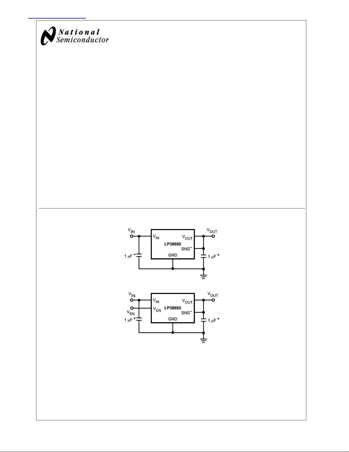
Typical Application Circuits
Features
n 2.5% output accuracy (25˚C)
n Low dropout voltage: 450mV
n Wide input voltage range (2.7V to 10V)
n Precision (trimmed) bandgap reference
n Guaranteed specs for -40˚C to +125˚C
n 1µA off-state quiescent current
n Thermal overload protection
n Foldback current limiting
n T0-252, SOT-223 and 6-Lead LLP packages
n Enable pin (LP38692)
@
1A (typ, 5V out)
Applications
n Hard Disk Drives
n Notebook Computers
n Battery Powered Devices
n Portable Instrumentation
20126601
20126602
Note: * Minimum value required for stability.
**LLP package devices only.
© 2005 National Semiconductor Corporation DS201266 www.national.com
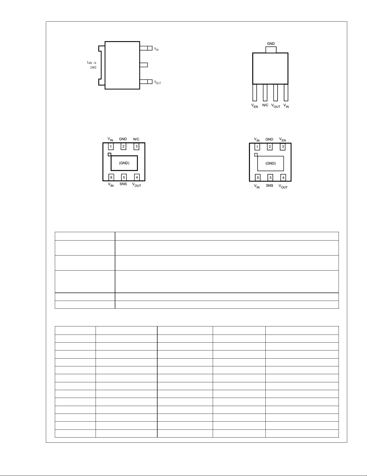
Connection Diagrams
LP38690/LP38692
TO-252, Top View
LP38690DT-X.X
6-Lead LLP, Bottom View
LP38690SD-X.X
Pin Description
PIN DESCRIPTION
V
IN
GND Circuit ground for the regulator. This is connected to the die through the lead frame, and also
SNS Output sense pin allows remote sensing at the load which will eliminate the error in output
V
EN
V
OUT
20126603
20126604
SOT-223, Top View
LP38692MP-X.X
20126605
20126606
6-Lead LLP, Bottom View
LP38692SD-X.X
This is the input supply voltage to the regulator. For LLP devices, both VINpins must be tied
together for full current operation (500mA maximum per pin).
functions as the heat sink when the large ground pad is soldered down to a copper plane.
voltage due to voltage drops caused by the resistance in the traces between the regulator and
the load. This pin must be tied to V
OUT
.
The enable pin allows the part to be turned ON and OFF by pulling this pin high or low.
Regulated output voltage.
Ordering Information
Order Number Package Marking Package Type Package Drawing Supplied As
LP38690SD-1.8 L113B 6-Lead LLP SDE06A 1000 Units Tape and Reel
LP38690SD-2.5 L114B 6-Lead LLP SDE06A 1000 Units Tape and Reel
LP38690SD-3.3 L115B 6-Lead LLP SDE06A 1000 Units Tape and Reel
LP38690SD-5.0 L116B 6-Lead LLP SDE06A 1000 Units Tape and Reel
LP38690DT-1.8 LP38690DT-1.8 TO-252 TD03B Available Soon
LP38690DT-2.5 LP38690DT-2.5 TO-252 TD03B Available Soon
LP38690DT-3.3 LP38690DT-3.3 TO-252 TD03B Available Soon
LP38690DT-5.0 LP38690DT-5.0 TO-252 TD03B Available Soon
LP38692SD-1.8 L123B 6-Lead LLP SDE06A 1000 Units Tape and Reel
LP38692SD-2.5 L124B 6-Lead LLP SDE06A 1000 Units Tape and Reel
LP38692SD-3.3 L125B 6-Lead LLP SDE06A 1000 Units Tape and Reel
LP38692SD-5.0 L126B 6-Lead LLP SDE06A 1000 Units Tape and Reel
LP38692MP-1.8 LJPB SOT-223 MP05A 1000 Units Tape and Reel
www.national.com 2
Ordering Information (Continued)
Order Number Package Marking Package Type Package Drawing Supplied As
LP38692MP-2.5 LJRB SOT-223 MP05A 1000 Units Tape and Reel
LP38692MP-3.3 LJSB SOT-223 MP05A 1000 Units Tape and Reel
LP38692MP-5.0 LJTB SOT-223 MP05A 1000 Units Tape and Reel
LP38690SDX-1.8 L113B 6-Lead LLP SDE06A 4500 Units Tape and Reel
LP38690SDX-2.5 L114B 6-Lead LLP SDE06A 4500 Units Tape and Reel
LP38690SDX-3.3 L115B 6-Lead LLP SDE06A 4500 Units Tape and Reel
LP38690SDX-5.0 L116B 6-Lead LLP SDE06A 4500 Units Tape and Reel
LP38690DTX-1.8 LP38690DT-1.8 TO-252 TD03B Available Soon
LP38690DTX-2.5 LP38690DT-2.5 TO-252 TD03B Available Soon
LP38690DTX-3.3 LP38690DT-3.3 TO-252 TD03B Available Soon
LP38690DTX-5.0 LP38690DT-5.0 TO-252 TD03B Available Soon
LP38692SDX-1.8 L123B 6-Lead LLP SDE06A 4500 Units Tape and Reel
LP38692SDX-2.5 L124B 6-Lead LLP SDE06A 4500 Units Tape and Reel
LP38692SDX-3.3 L125B 6-Lead LLP SDE06A 4500 Units Tape and Reel
LP38692SDX-5.0 L126B 6-Lead LLP SDE06A 4500 Units Tape and Reel
LP38692MPX-1.8 LJPB SOT-223 MP05A 2000 Units Tape and Reel
LP38692MPX-2.5 LJRB SOT-223 MP05A 2000 Units Tape and Reel
LP38692MPX-3.3 LJSB SOT-223 MP05A 2000 Units Tape and Reel
LP38692MPX-5.0 LJTB SOT-223 MP05A 2000 Units Tape and Reel
LP38690/LP38692
www.national.com3
Absolute Maximum Ratings (Note 1)
If Military/Aerospace specified devices are required,
please contact the National Semiconductor Sales Office/
Distributors for availability and specifications.
Storage Temperature Range −65˚C to +150˚C
Lead Temp. (Soldering, 5 seconds) 260˚C
LP38690/LP38692
ESD Rating (Note 3) 2 kV
Power Dissipation (Note 2) Internally Limited
V(max) All pins (with respect to GND) -0.3V to 12V
I
OUT
Internally Limited
Junction Temperature −40˚C to +150˚C
Operating Ratings
VINSupply Voltage 2.7V to 10V
Operating Junction
Temperature Range
−40˚C to +125˚C
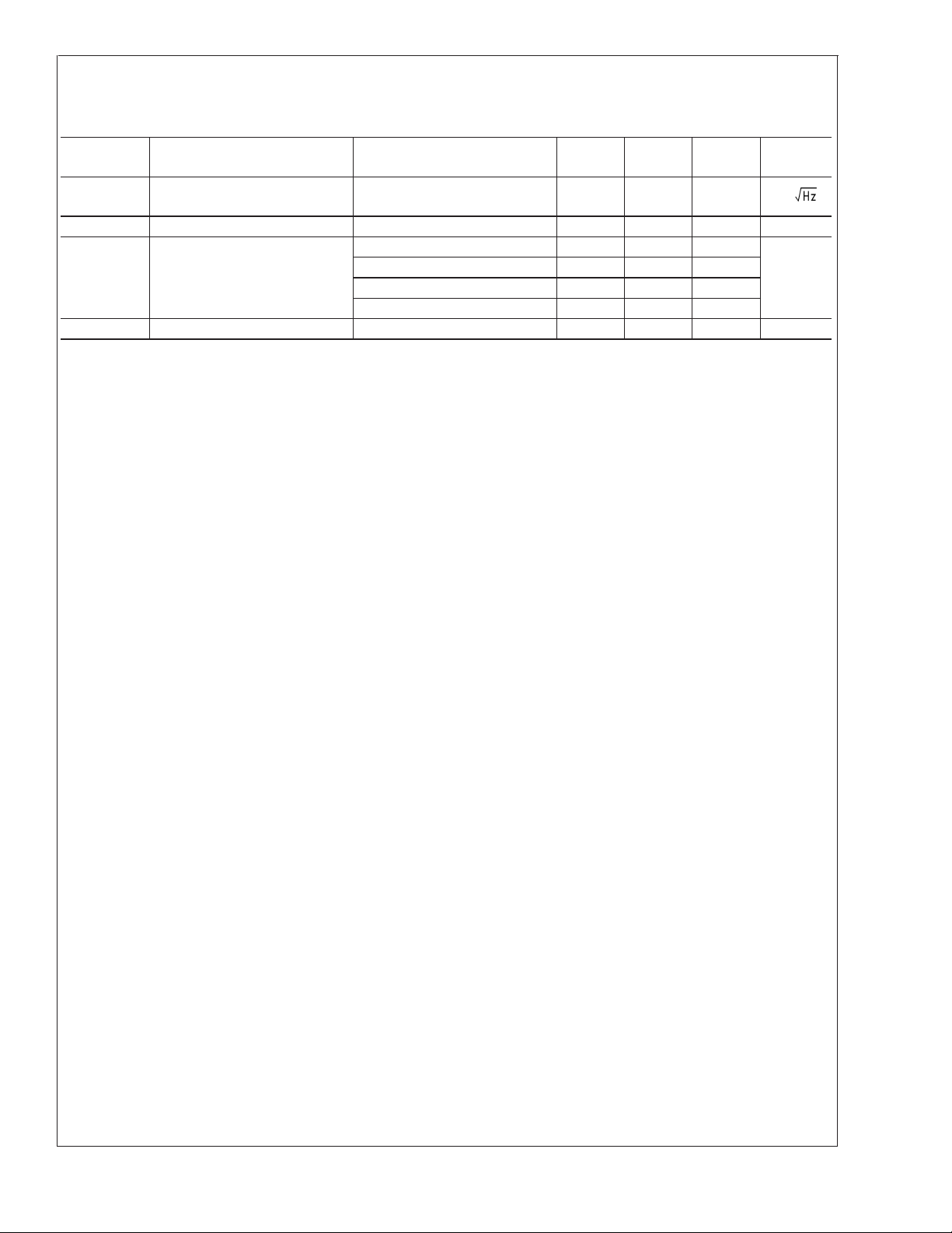
Electrical Characteristics Limits in standard typeface are for T
over the full operating temperature range. Unless otherwise specified: V
IN=VOUT
= 25˚C, and limits in boldface type apply
J
+ 1V, CIN=C
OUT
= 10 µF, I
Min/Max limits are guaranteed through testing, statistical correlation, or design.
Symbol Parameter Conditions MIN
TYP
(Note 4)
-2.5 2.5
V
O
∆V
/∆V
O
∆V
/∆I
O
L
V
IN-VOUT
I
Q
I
(MIN) Minimum Load Current VIN-VO≤ 4V 100
L
I
FB
PSRR Ripple Rejection V
T
SD
(HYST) Thermal Shutdown Hysteresis
T
SD
Output Voltage Tolerance
Output Voltage Line Regulation
IN
(Note 6)
Output Voltage Load Regulation
(Note 7)
Dropout Voltage (Note 8)
100 µA<I
+1V≤ VIN≤ 10V
V
O
VO+ 0.5V ≤ VIN≤ 10V
= 25mA
I
L
1mA<I
V
IN=VO
= 1.8V)
(V
O
=1A
I
L
= 2.5V)
(V
O
= 0.1A
I
L
=1A
I
L
(V
= 3.3V)
O
= 0.1A
I
L
=1A
I
L
(V
= 5V)
O
= 0.1A
I
L
=1A
I
L
L
<
L
+1V
<
1A
1A
-5.0 5.0
Quiescent Current VIN≤ 10V, IL=100 µA - 1A 55 100
≤ 0.4V, (LP38692 Only) 0.001 1
EN
IN-VO
IN=VO
>
5V 450
O
<
4V 1500
+ 2V(DC), with 1V(p-p)
Foldback Current Limit VIN-V
V
/ 120Hz Ripple
Thermal Shutdown Activation
(Junction Temp)
(Junction Temp)
0.03 0.1 %/V
1.8 5 %/A
950 1600
80
800
65
650
45
450
55 dB
160
10
= 10mA.
LOAD
MAX Units
%V
OUT
145
1300
110
mV
1000
100
800
µAV
mA
˚C
www.national.com 4
LP38690/LP38692
Electrical Characteristics Limits in standard typeface are for T
over the full operating temperature range. Unless otherwise specified: V
IN=VOUT
= 25˚C, and limits in boldface type apply
J
+ 1V, CIN=C
OUT
= 10 µF, I
LOAD
= 10mA.
Min/Max limits are guaranteed through testing, statistical correlation, or design. (Continued)
Symbol Parameter Conditions MIN
e
n
VO(LEAK) Output Leakage Current VO=VO(NOM) + 1V@10V
V
EN
I
EN
Note 1: Absolute maximum ratings indicate limits beyond which damage to the component may occur. Operating ratings indicate conditions for which the device
is intended to be functional, but do not guarantee specific performance limits. For guaranteed specifications, see Electrical Characteristics. Specifications do not
apply when operating the device outside of its rated operating conditions.
Note 2: At elevated temperatures, device power dissipation must be derated based on package thermal resistance and heatsink values (if a heatsink is used). The
junction-to-ambient thermal resistance ( θ
area (less than 0.1 square inch). If one square inch of copper is used as a heat dissipator for the TO-252, the θ
package has a θ
to a copper area of one square inch. The θ
(refer to application note AN-1187). If power disspation causes the junction temperature to exceed specified limits, the device will go into thermal shutdown.
Note 3: ESD is tested using the human body model which is a 100pF capacitor discharged through a 1.5k resistor into each pin.
Note 4: Typical numbers represent the most likely parametric norm for 25˚C operation.
Note 5: If used in a dual-supply system where the regulator load is returned to a negative supply, the output pin must be diode clamped to ground.
Note 6: Output voltage line regulation is defined as the change in output voltage from nominal value resulting from a change in input voltage.
Note 7: Output voltage load regulation is defined as the change in output voltage from nominal value as the load current increases from 1mA to full load.
Note 8: Dropout voltage is defined as the minimum input to output differential required to maintain the output within 100mV of nominal value.
Output Noise BW = 10Hz to 10kHz
= 3.3V
V
O
IN
Enable Voltage (LP38692 Only) Output = OFF 0.4
Output = ON, V
Output = ON, V
Output = ON, V
=4V 1.8
IN
=6V 3.0
IN
= 10V 4.0
IN
Enable Pin Leakage VEN= 0V or 10V, VIN= 10V -1 0.001 1 µA
) for the TO-252 is approximately 90˚C/W for a PC board mounting with the device soldered down to minimum copper
J-A
of approximately 125˚C/W when soldered down to a minimum sized pattern (less than 0.1 square inch) and approximately 70˚C/W when soldered
J-A
values for the LLP package are also dependent on trace area, copper thickness, and the number of thermal vias used
J-A
J-A
TYP
(Note 4)
MAX Units
0.7 µV/
0.5 12 µA
drops to approximately 50˚C/W. The SOT-223
V
www.national.com5

Block Diagrams
LP38690/LP38692
20126607
FIGURE 1. LP38690 Functional Diagram (LLP)
FIGURE 2. LP38690 Functional Diagram (TO-252)
www.national.com 6
20126608

Block Diagrams (Continued)
FIGURE 3. LP38692 Functional Diagram (LLP)
LP38690/LP38692
20126609
FIGURE 4. LP38692 Functional Diagram (SOT-223)
20126610
www.national.com7

Typical Performance Characteristics Unless otherwise specified: T
enable pin is tied to V
LP38690/LP38692
(LP38692 only), V
IN
Noise vs Frequency Noise vs Frequency
= 1.8V, VIN=V
OUT
+1V, IL= 10mA.
OUT
= 25˚C, CIN=C
J
OUT
=10µF,
20126635
Noise vs Frequency Ripple Rejection
20126637
Ripple Rejection Ripple Rejection
20126636
20126618
20126620 20126622
www.national.com 8

LP38690/LP38692
Typical Performance Characteristics Unless otherwise specified: T
enable pin is tied to V
Line Transient Response Line Transient Response
Line Transient Response Load Transient Response
(LP38692 only), V
IN
= 1.8V, VIN=V
OUT
20126624 20126626
+1V, IL= 10mA. (Continued)
OUT
= 25˚C, CIN=C
J
OUT
=10µF,
20126628
Load Transient Response Load Transient Response
20126641 20126642
20126640
www.national.com9

Typical Performance Characteristics Unless otherwise specified: T
enable pin is tied to V
LP38690/LP38692
V
(LP38692 only), V
IN
Load Transient Response Load Transient Response
vs Temperature (5.0V) V
OUT
= 1.8V, VIN=V
OUT
20126643 20126644
+1V, IL= 10mA. (Continued)
OUT
= 25˚C, CIN=C
J
vs Temperature (3.3V)
OUT
OUT
=10µF,
20126630
V
vs Temperature (2.5V) V
OUT
20126632 20126633
www.national.com 10
vs Temperature (1.8V)
OUT
20126631

LP38690/LP38692
Typical Performance Characteristics Unless otherwise specified: T
enable pin is tied to V
Dropout Voltage vs I
Enable Voltage vs Temperature Load Regulation vs Temperature
(LP38692 only), V
IN
OUT
OUT
= 1.8V, VIN=V
+1V, IL= 10mA. (Continued)
OUT
Dropout Voltage vs I
20126650 20126651
= 25˚C, CIN=C
J
OUT
OUT
=10µF,
Line Regulation vs Temperature
20126652 20126653
20126654
www.national.com11

Application Hints
EXTERNAL CAPACITORS
Like any low-dropout regulator, external capacitors are required to assure stability. These capacitors must be correctly
selected for proper performance.
LP38690/LP38692
INPUT CAPACITOR: An input capacitor of at least 1µF is
required (ceramic recommended). The capacitor must be
located not more than one centimeter from the input pin and
returned to a clean analog ground.
OUTPUT CAPACITOR: An output capacitor is required for
loop stability. It must be located less than 1 centimeter from
the device and connected directly to the output and ground
pins using traces which have no other currents flowing
through them.
The minimum amount of output capacitance that can be
used for stable operation is 1µF. Ceramic capacitors are
recommended (the LP38690/2 was designed for use with
ultra low ESR capacitors). The LP38690/2 is stable with any
output capacitor ESR between zero and 100 Ohms.
ENABLE PIN (LP38692 only): The LP38692 has an enable
pin which turns the regulator output on and off. Pulling the
enable pin down to a logic low will turn the part off. The
voltage the pin has to be pulled up to in order to assure the
part is on depends on input voltage (refer to Electrical Characteristics section). This pin should be tied to V
enable function is not used.
Foldback Current Limiting: Foldback current limiting is
built into the LP38690/2 which reduces the amount of output
current the part can deliver as the output voltage is reduced.
The amount of load current is dependent on the differential
voltage between V
IN
and V
tial voltage exceeds 5V, the load current will limit at about
450 mA. When the V
IN-VOUT
4V, load current is limited to about 1500 mA.
SELECTING A CAPACITOR
It is important to note that capacitance tolerance and variation with temperature must be taken into consideration when
selecting a capacitor so that the minimum required amount
of capacitance is provided over the full operating temperature range.
Capacitor Characteristics
CERAMIC: For values of capacitance in the 10 to 100 µF
range, ceramics are usually larger and more costly than
tantalums but give superior AC performance for bypassing
high frequency noise because of very low ESR (typically less
than 10 mΩ). However, some dielectric types do not have
good capacitance characteristics as a function of voltage
and temperature.
Z5U and Y5V dielectric ceramics have capacitance that
drops severely with applied voltage. A typical Z5U or Y5V
capacitor can lose 60% of its rated capacitance with half of
the rated voltage applied to it. The Z5U and Y5V also exhibit
a severe temperature effect, losing more than 50% of nominal capacitance at high and low limits of the temperature
range.
X7R and X5R dielectric ceramic capacitors are strongly recommended if ceramics are used, as they typically maintain a
capacitance range within
ing ratings of temperature and voltage. Of course, they are
typically larger and more costly than Z5U/Y5U types for a
given voltage and capacitance.
. Typically, when this differen-
OUT
differential is reduced below
±
20% of nominal over full operat-
IN
if the
TANTALUM: Solid Tantalum capacitors have good temperature stability: a high quality Tantalum will typically show a
capacitance value that varies less than 10-15% across the
full temperature range of -40˚C to +125˚C. ESR will vary only
about 2X going from the high to low temperature limits.
PCB LAYOUT
Good PC layout practices must be used or instability can be
induced because of ground loops and voltage drops. The
input and output capacitors must be directly connected to the
input, output, and ground pins of the regulator using traces
which do not have other currents flowing in them (Kelvin
connect).
The best way to do this is to lay out C
device with short traces to the V
IN,VOUT
IN
and C
OUT
near the
, and ground pins.
The regulator ground pin should be connected to the external circuit ground so that the regulator and its capacitors
have a "single point ground".
It should be noted that stability problems have been seen in
applications where "vias" to an internal ground plane were
used at the ground points of the IC and the input and output
capacitors. This was caused by varying ground potentials at
these nodes resulting from current flowing through the
ground plane. Using a single point ground technique for the
regulator and it’s capacitors fixed the problem. Since high
current flows through the traces going into V
from V
, Kelvin connect the capacitor leads to these pins
OUT
and coming
IN
so there is no voltage drop in series with the input and output
capacitors.
RFI/EMI SUSCEPTIBILITY
RFI (radio frequency interference) and EMI (electromagnetic
interference) can degrade any integrated circuit’s performance because of the small dimensions of the geometries
inside the device. In applications where circuit sources are
present which generate signals with significant high fre-
>
quency energy content (
1 MHz), care must be taken to
ensure that this does not affect the IC regulator.
If RFI/EMI noise is present on the input side of the regulator
(such as applications where the input source comes from the
output of a switching regulator), good ceramic bypass capacitors must be used at the input pin of the IC.
If a load is connected to the IC output which switches at high
speed (such as a clock), the high-frequency current pulses
required by the load must be supplied by the capacitors on
the IC output. Since the bandwidth of the regulator loop is
less than 100 kHz, the control circuitry cannot respond to
load changes above that frequency. This means the effective
output impedance of the IC at frequencies above 100 kHz is
determined only by the output capacitor(s).
In applications where the load is switching at high speed, the
output of the IC may need RF isolation from the load. It is
recommended that some inductance be placed between the
output capacitor and the load, and good RF bypass capacitors be placed directly across the load.
PCB layout is also critical in high noise environments, since
RFI/EMI is easily radiated directly into PC traces. Noisy
circuitry should be isolated from "clean" circuits where possible, and grounded through a separate path. At MHz frequencies, ground planes begin to look inductive and RFI/
EMI can cause ground bounce across the ground plane. In
multi-layer PCB applications, care should be taken in layout
so that noisy power and ground planes do not radiate directly
into adjacent layers which carry analog power and ground.
www.national.com 12

Application Hints (Continued)
OUTPUT NOISE
Noise is specified in two ways: Spot Noise or Output Noise
Density is the RMS sum of all noise sources, measured at
the regulator output, at a specific frequency (measured with
a 1Hz bandwidth). This type of noise is usually plotted on a
curve as a function of frequency. Total Output Noise or
Broad-Band Noise is the RMS sum of spot noise over a
specified bandwidth, usually several decades of frequencies.
LP38690/LP38692
Attention should be paid to the units of measurement. Spot
noise is measured in units µV/root-Hz or nV/root-Hz and total
output noise is measured in µV(rms)
The primary source of noise in low-dropout regulators is the
internal reference. Noise can be reduced in two ways: by
increasing the transistor area or by increasing the current
drawn by the internal reference. Increasing the area will
decrease the chance of fitting the die into a smaller package.
Increasing the current drawn by the internal reference increases the total supply current (ground pin current).
www.national.com13

Physical Dimensions inches (millimeters) unless otherwise noted
LP38690/LP38692
6-lead, LLP Package
NS Package Number SDE06A
TO-252 Package
NS Package Number TD03B
www.national.com 14

Physical Dimensions inches (millimeters) unless otherwise noted (Continued)
LP38690/LP38692 1A Low Dropout CMOS Linear Regulators
Stable with Ceramic Output Capacitors
SOT-223 Package
NS Package Number MP05A
National does not assume any responsibility for use of any circuitry described, no circuit patent licenses are implied and National reserves
the right at any time without notice to change said circuitry and specifications.
For the most current product information visit us at www.national.com.
LIFE SUPPORT POLICY
NATIONAL’S PRODUCTS ARE NOT AUTHORIZED FOR USE AS CRITICAL COMPONENTS IN LIFE SUPPORT DEVICES OR SYSTEMS
WITHOUT THE EXPRESS WRITTEN APPROVAL OF THE PRESIDENT AND GENERAL COUNSEL OF NATIONAL SEMICONDUCTOR
CORPORATION. As used herein:
1. Life support devices or systems are devices or systems
which, (a) are intended for surgical implant into the body, or
(b) support or sustain life, and whose failure to perform when
properly used in accordance with instructions for use
2. A critical component is any component of a life support
device or system whose failure to perform can be reasonably
expected to cause the failure of the life support device or
system, or to affect its safety or effectiveness.
provided in the labeling, can be reasonably expected to result
in a significant injury to the user.
BANNED SUBSTANCE COMPLIANCE
National Semiconductor certifies that the products and packing materials meet the provisions of the Customer Products Stewardship
Specification (CSP-9-111C2) and the Banned Substances and Materials of Interest Specification (CSP-9-111S2) and contain no ‘‘Banned
Substances’’ as defined in CSP-9-111S2.
National Semiconductor
Americas Customer
Support Center
Email: new.feedback@nsc.com
Tel: 1-800-272-9959
www.national.com
National Semiconductor
Europe Customer Support Center
Fax: +49 (0) 180-530 85 86
Email: europe.support@nsc.com
Deutsch Tel: +49 (0) 69 9508 6208
English Tel: +44 (0) 870 24 0 2171
Français Tel: +33 (0) 1 41 91 8790
National Semiconductor
Asia Pacific Customer
Support Center
Email: ap.support@nsc.com
National Semiconductor
Japan Customer Support Center
Fax: 81-3-5639-7507
Email: jpn.feedback@nsc.com
Tel: 81-3-5639-7560
 Loading...